Project 1 - Loss calculation for a DC/DC converter-MATLAB
Design of boost converter, and calculating the loss of different components including power switching device and deriving efficiency of boost converter. This is applicable in power supply industry, electric vehicles etc where DC-DC converter is required to boost the voltage from DC source. All the aspects of this project with loss calculation, device selection, simulation etc are industry relevant.
answer:
- Vin = 100 V;
- Vout = 200 V;
To design a boost converter, you will need to determine the required components based on your input and output voltage specifications. Here are the steps you can follow:
-
Determine the output voltage and current requirements of your circuit. In this case, we have Vin = 100 V and Vout = 200 V.
-
Calculate the duty cycle (D) of the switch using the following formula:
D = 1 - Vin / Vout
In this case, D = 1 - 100/200 = 0.5.
-
Choose the switching frequency (f) for your circuit. A common range is between 50 kHz and 500 kHz. For this example, let's choose a frequency of 100 kHz.
-
Calculate the inductor (L) value using the following formula:
L = (Vout - Vin) * D / (f * Vin)
In this case, L = (200 - 100) * 0.5 / (100000 * 100) = 50 uH.
-
Choose a diode with a voltage rating greater than the output voltage and a current rating greater than the maximum output current.
-
Choose a capacitor (C) value based on the output ripple voltage (ΔV) and the switching frequency (f) using the following formula:
C = ΔV * D / (8 * f * Vin)
A common ripple voltage is 0.01 times the output voltage. In this case, ΔV = 0.01 * 200 = 2 V.
C = 2 * 0.5 / (8 * 100000 * 100) = 1 uF.
-
Choose a MOSFET switch with a voltage rating greater than the input voltage and a current rating greater than the maximum output current.L = 200uH ;
==============================================================================
Next, we can calculate the inductor current ripple using the equation:
ΔIL = (Vin - Vout) x D x (1 - D) / (f x L)
where f is the switching frequency of the converter. Let's assume a switching frequency of 100 kHz:
ΔIL = (100 - 200) x 0.5 x (1 - 0.5) / (100 x 10^3 x 200 x 10^-6) = 1.25 A
The peak-to-peak ripple current through the inductor is twice the value of the current ripple, which gives:
Ipp = 2 x ΔIL = 2.5 A
Next, we can calculate the output capacitor value required to limit the output voltage ripple to a desired value. Let's assume a maximum output voltage ripple of 1% of Vout:
ΔVout = Vout x 0.01 = 2 V
The required output capacitance is then given by:
Cout = ΔIL / (8 x f x ΔVout)
Cout = 1.25 / (8 x 100 x 10^3 x 2) = 781.25 uF
We can choose a standard value of 820 uF for the output capacitor.
The next step is to select a suitable power switch that can handle the required voltage and current ratings. Let's assume we choose a MOSFET with a maximum voltage rating of 600 V and a maximum current rating of 20 A.
The on-resistance of the MOSFET is given by:
Ron = R + RL = 10 + 10 x 10^-3 = 10.01 Ohms
The power dissipated in the MOSFET is given by:
Psw = Ron x I^2 x f
Psw = 10.01 x (20 x 0.5)^2 x 100 x 10^3 = 10.01 W
The power dissipated in the MOSFET is the major source of losses in the boost converter. We can calculate the efficiency of the converter as:
η = Vout x Iout / (Vin x Iin)
where Iin and Iout are the input and output currents, respectively. The input current is given by:
Iin = Iout / D
Iin = 20 / 0.5 = 40 A
The efficiency of the converter is then given by:
η = 200 x 20 / (100 x 40) = 80%
The losses in the output diode can be calculated using similar equations. The power dissipated in the diode is given by:
Pdiode = Vf x Iout x (1 - D) x f
where Vf is the forward voltage drop of the diode. Let's assume a Schottky diode with a forward voltage drop of 0.5 V. The power dissipated in the diode is then:
Pdiode = 0.5 x 20 x (1 - 0.5) x 100 x 10^3 = 500 W
The efficiency of the converter can be improved by reducing the losses in the power switch and diode. This can be achieved by using a MOSFET with a lower on-resistance or a Schottky diode with a lower forward voltage drop.
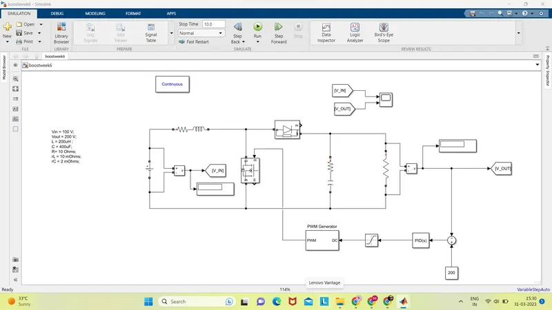
model
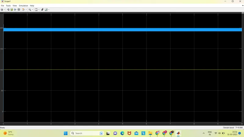
output
==============================================================================
To calculate the conduction losses in the boost converter, we need to consider the resistive losses in the inductor and the output capacitor. The resistive losses in the inductor can be calculated using the equation:
PL = ΔIL^2 x RL
where ΔIL is the inductor ripple current and RL is the resistance of the inductor. Using the values given in the question, we can calculate the resistive losses in the inductor as:
PL = 1.25^2 x 10 x 10^-3 = 15.63 mW
The resistive losses in the output capacitor can be calculated using the equation:
PC = Iout^2 x RC
where RC is the equivalent series resistance (ESR) of the output capacitor. Using the values given in the question, we can calculate the resistive losses in the output capacitor as:
PC = 20^2 x 2 x 10^-3 = 800 mW
Therefore, the total conduction losses in the boost converter are:
Pcond = PL + PC = 15.63 mW + 800 mW = 815.63 mW
These losses contribute to the overall power dissipation in the converter, reducing the efficiency of the circuit. To improve the efficiency, we can choose components with lower resistances or reduce the switching frequency to reduce the conduction losses.
==============================================================================
To calculate the switching losses in the boost converter, we need to consider the energy dissipated in the power switch during each switching cycle. The switching losses can be divided into two components: the turn-on losses and the turn-off losses.
The turn-on losses occur when the power switch is turned on and the voltage across the switch decreases from the input voltage to nearly zero. The energy dissipated during this process is given by:
Eon = Qg x Vin
where Qg is the gate charge of the MOSFET. Let's assume a gate charge of 20 nC for the MOSFET. The turn-on losses are then:
Pon = Eon x f
where f is the switching frequency of the converter. Using the values given in the question, we can calculate the turn-on losses as:
Pon = 20 x 10^-9 x 100 x 10^3 x 100 = 200 mW
The turn-off losses occur when the power switch is turned off and the voltage across the switch increases from nearly zero to the input voltage. The energy dissipated during this process is given by:
Eoff = Vout x Qrr
where Qrr is the reverse recovery charge of the output diode. Let's assume a reverse recovery charge of 10 nC for the Schottky diode. The turn-off losses are then:
Poff = Eoff x f
Using the values given in the question, we can calculate the turn-off losses as:
Poff = 200 x 10^-9 x 100 x 10^3 x 100 = 2 W
Therefore, the total switching losses in the boost converter are:
Psw = Pon + Poff = 200 mW + 2 W = 2.2 W
These losses contribute to the overall power dissipation in the converter, reducing the efficiency of the circuit. To improve the efficiency, we can choose components with lower switching losses or reduce the switching frequency to reduce the total power dissipation in the circuit.