Week 9 - PCB Thermal Simulation
Aim:
The PCB model is created by importing the PCB layout, files and traces to ANSYS Icepak - and perform thermal analysis of the same for the following three cases:
1. The model is solved only for conduction, without the components.
2. The model is solved for forced convection with the actual components.
3. The model is solved for forced convection and trace heating.
Introduction:
In the current project, the following tasks are performed:
1. The given board file, which contains information about the different components on the PCB, is imported to ANSYS Icepak. The associated library file gets automatically populated.
2. The given ECAD file, which contains information about the trace layers and vias present on the PCB, is imported to ANSYS Icepak.
3. The model is solved for conduction only without the actual components.
4. The model is solved for forced convection with the actual components.
5. The model is solved for forced convection with the actual components and the joule-heating within the trace layers of the PCB is modeled.
PCB supports the different electronic components in an electronic assembly. Generally a PCB is made up of alternate layers of an electrically conducting material (say copper) and a dielectric material (say FR4) along its thickness. The electrically conducting pathways transmit electrical signals between components, and are known as traces or trace-layers. Two trace-layers are separated by dielectric material and are connected by electrically conducting (generally hollow) cylinders, known as vias. Apart from providing electrical connectivity a vias also allows air-flow through the PCB which results in cooling. The image attached below shows a general PCB.

Since the trace-layers are made up of electrically conducting material with finite electrical resistance, they generate heat as current passes through them. Modeling the trace-heating accurately is quite important if one is interested in predicting the thermal performance of the PCB and hence simulations similar to the one performed in the current project are often performed by the thermal engineers in the electronics industry.
1.Conduction-only model:
Geometry:
The image attached below shows the geometry of the model.

It can be seen that all the components on PCB are deactivated and the cabinet is rescaled to the dimensions of the PCB.
Meshing:
The computational domain is discretized using the Hex-dominant grid generated by the "Mesher-HD". The maximum element sizes along the X, Y and Z directions are set to 2.032 mm, 2.032 mm and 0.05 mm respectively. The minimum gaps along the X, Y and Z directions are set to 1 mm, 1 mm and 0.01 mm respectively. The image attached below shows the "Mesh control" window.
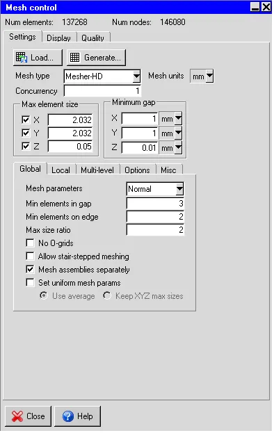
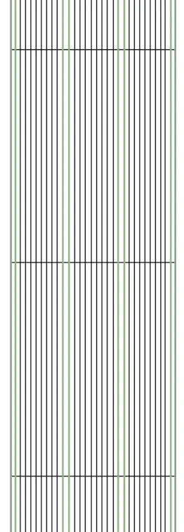
It can be seen that the generated mesh yields 137268 elements and 146080 nodes. The images attached below show the computational mesh plotted on three mutually perpendicular planes, each passing through the center of the cabinet.
X-plane:
Y-plane:

Z-plane:

Visually the mesh appears to be fine. The images attached below show the histograms with the number of elements plotted along the X-axis and the quality measures plotted along the Y-axis.
1. Face-alignment
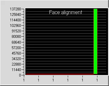
Values less than 0.05 indicate the presence of severely distorted elements in the mesh. All the elements in the current mesh have a face-alignment of 1 which indicates that they are perfectly aligned to each other.
2. Volume
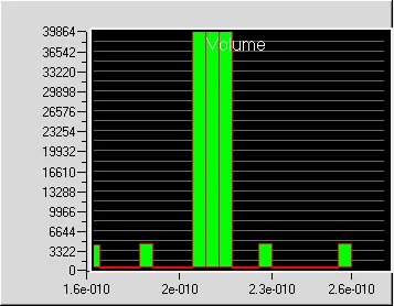
For a double precision solver the minimum cell volume should not be less than 1e-15 m^3 otherwise the solver may face issues. The minimum cell volume in the current mesh is 1.64139e-10 m^3 and hence the mesh elements aren't small enough to cause problems in the solver.
3. Skewness
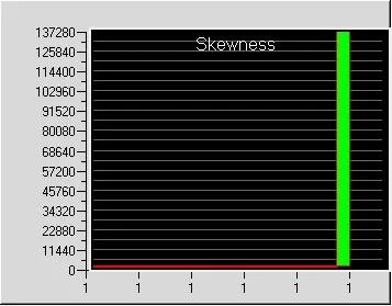
A skewness of 0 indicates that the mesh element is degenerate whereas a skewness of 1 indicates that it is ideal (equilateral/equiangular). All the elements in the current mesh have a skewness of 1 which indicates that they are ideal (equilateral/equiangular).
Solver:
The three-dimensional steady-state Navier-Stokes equations for the model are solved within the computational domain for temperature field using the Fluent solver available in ANSYS Icepak. The following settings are applied to the solver:
1. Variables solved: Temperature
2. Radiation: Off
3. Time variation: Steady
4. Solution initialization
4.1. Temperature: Ambient (20 deg. C)
5. Number of iterations: 500
6. Convergence criteria
6.1. Energy: 1e-20
7. Configuration: Parallel
8. Number of processors: 4
9. GPU computing: Enabled
10. Number of GPUs: 1
11. Discretization scheme
11.1. Temperature: First
12. Under-relaxation factor
12.1. Temperature: 1
13. Linear solver settings
13.1. Temperature - Type: F, Tolerance criterion: 1e-6, Residual reduction tolerance: 1e-6, Stabilization: None
14. Precision: Double
Results:
In the current section, the simulation results are discussed.
Residuals:
The residuals for the energy equation are plotted against the number of iterations, as shown in the image attached below.
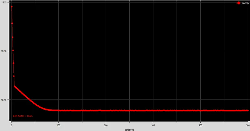
The plot shows that the residuals are quite small quantitatively and don't change appreciably between 300-500 iterations which indicates that the solution has reached a steady state. For the current model, the simulation results after 500 iterations are considered as steady-state results.
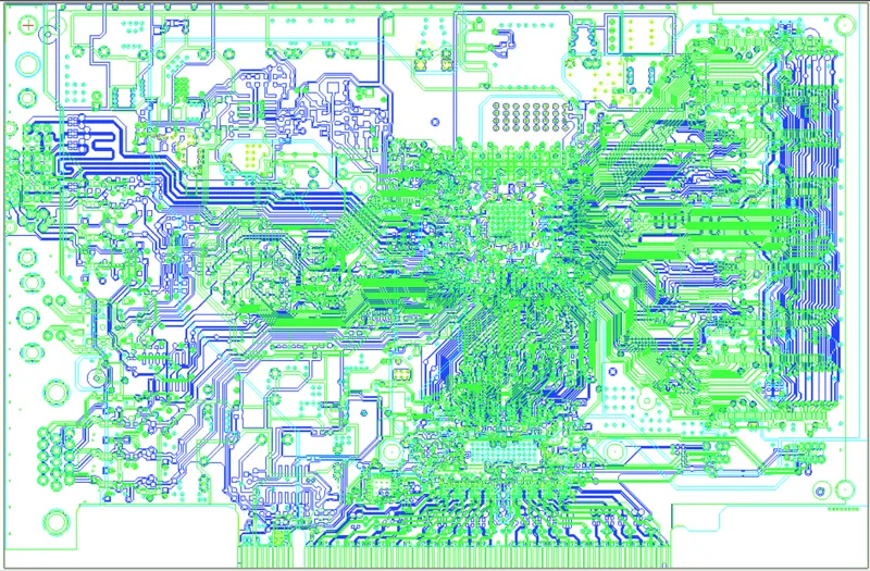
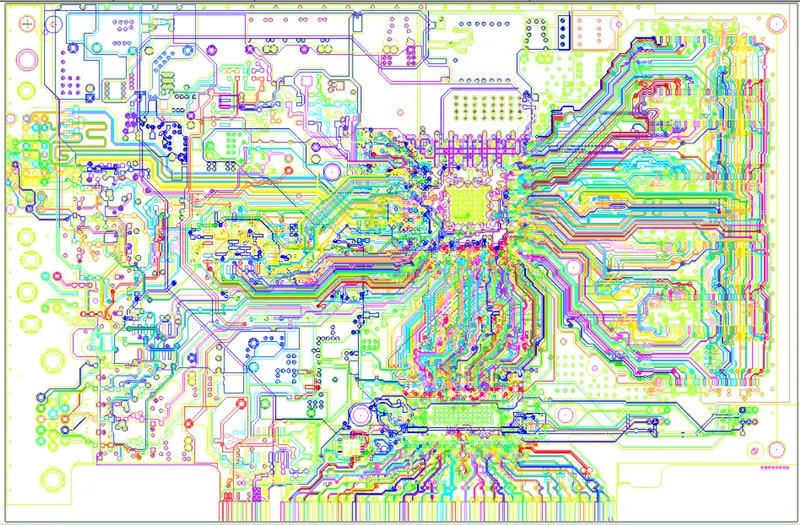
PCB-traces
The images attached below show the PCB-traces using different display options.
Single color
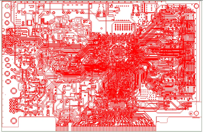
This option displays all the PCB-traces using a single color.
Color by trace
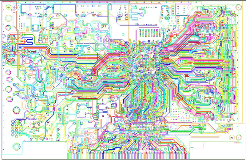
This option displays different PCB-traces using different colors.
Color by layer
Color by net
Metal fractions
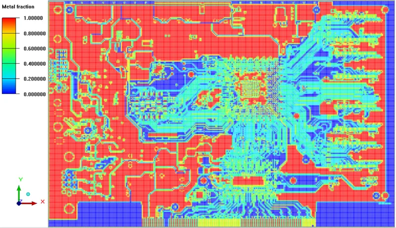
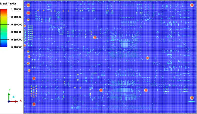
The images attached below show the metal fraction contours plotted over the different layers of the PCB.
Trace Layer_1:M1 Top
Trace Layer_2:D3
Trace Layer_3:M2
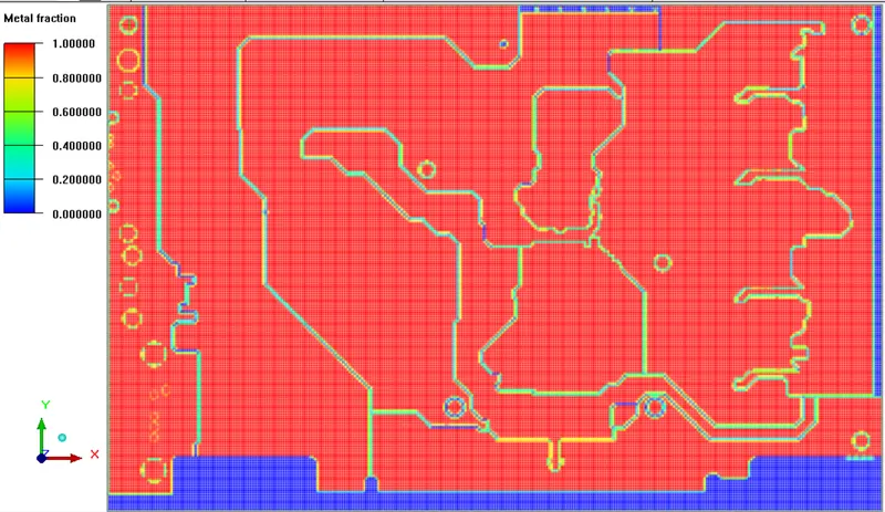
Trace Layer_4:M2
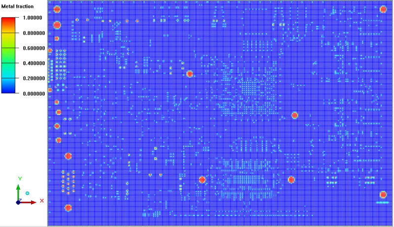
Trace Layer_5:M3
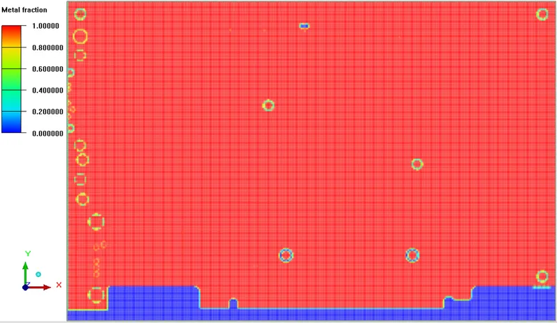
Trace Layer_6:D5
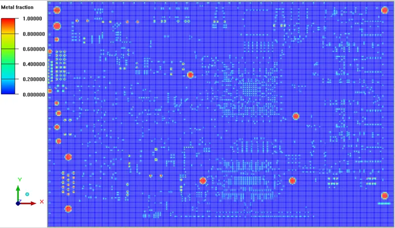
Trace Layer_7:M4
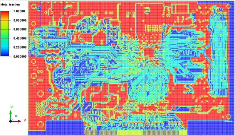
It is evident from the contours that a dielectric layer (with no copper traces) is sandwiched between two adjacent PCB layers that contain copper traces.
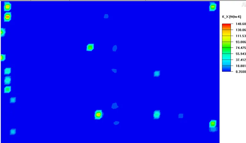
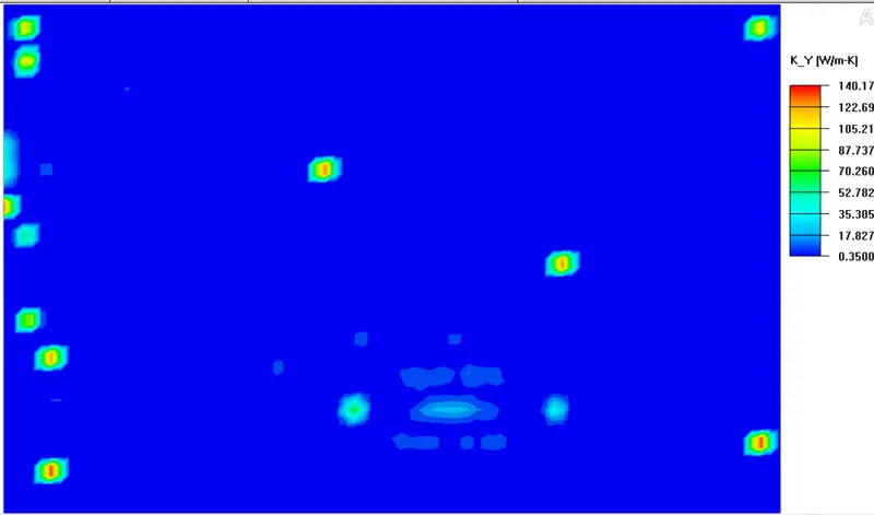
Thermal conductivity contours
The images attached below show the kx, kY and kZ thermal conductivity contours are plotted over the Z-plane passing through the center of the PCB.
kx contours:
ky contours:
kz contours:
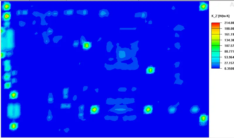
It is evident from the contours that the thermal conductivity of the PCB is anisotropic in nature.
Temperature contours:
The image attached below shows the steady-state temperature contours plotted over the Z-plane passing through the center of the PCB.
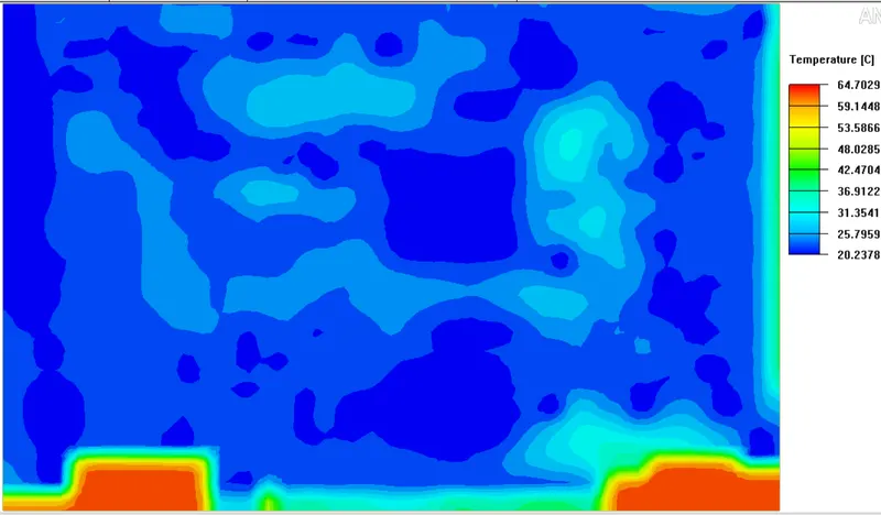
It is evident from the contour-legend that the maximum temperature on the plane is 64.703 deg. C.
2. Forced convection model:
Geometry:
The image attached below shows the geometry of the model.
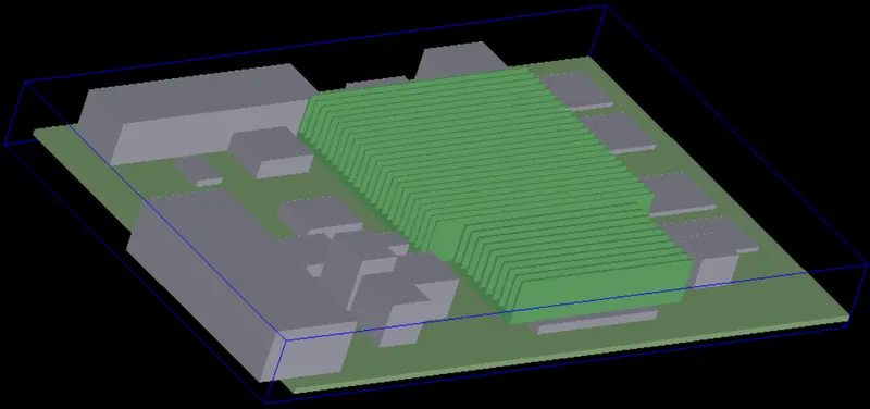
It can be seen that unlike the conduction-only model, a lot of components are activated in the model to perform forced convection analysis
Meshing:
The computational domain is discretized using the Hex-dominant grid generated by the "Mesher-HD". The maximum element sizes along the X, Y and Z directions are set to 9.5 mm, 5 mm and 0.7 mm respectively. The image attached below shows the "Mesh control" window.
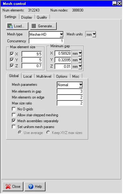
It can be seen that the generated mesh yields 312243 elements and 388830 nodes. The images attached below show the computational mesh plotted on three mutually perpendicular planes, each passing through the center of the cabinet.
X-plane:

Y-plane:

Z-plane:
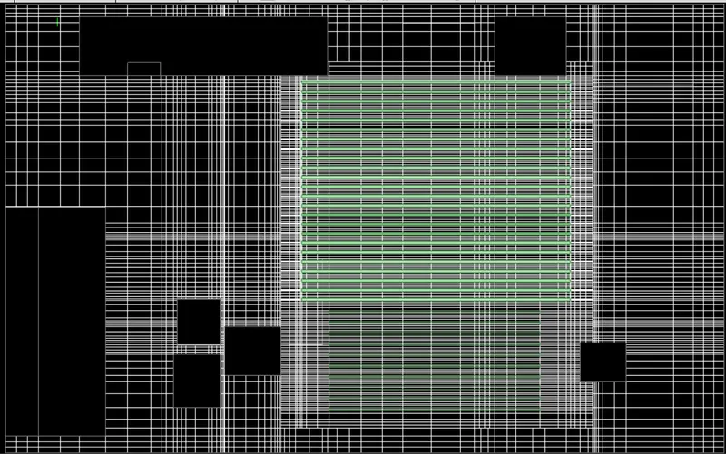
Visually the mesh appears to be fine. The images attached below show the histograms with the number of elements plotted along the X-axis and the quality measures plotted along the Y-axis.
1. Face-alignment
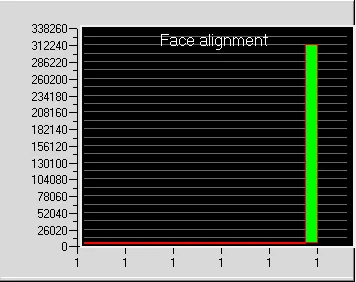
Values less than 0.05 indicate the presence of severely distorted elements in the mesh. All the elements in the current mesh have a face-alignment of 1 which indicates that they are perfectly aligned to each other.
2. Volume
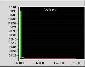
For a double precision solver the minimum cell volume should not be less than 1e-15 m^3 otherwise the solver may face issues. The minimum cell volume in the current mesh is 8.1161e-13 m^3 and hence the mesh elements aren't small enough to cause problems in the solver.
3. Skewness
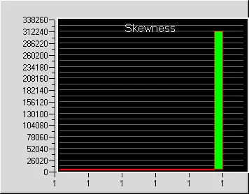
A skewness of 0 indicates that the mesh element is degenerate whereas a skewness of 1 indicates that they are ideal (equilateral/equiangular). All the elements in the current mesh have a skewness of 1 which indicates that they are ideal (equilateral/equiangular).
Solver:
The three-dimensional steady-state Navier-Stokes equations for the model are solved within the computational domain for flow and temperature field using the Fluent solver available in ANSYS Icepak. The following settings are applied to the solver:
1. Variables solved: Flow (velocity/pressure), Temperature
2. Radiation: Off
3. Time variation: Steady
4. Solution initialization
4.1. X velocity: -1 m/s
4.2. Y velocity: 0
4.3. Z velocity: 0
4.4. Temperature: Ambient (20 deg. C.)
5. Number of iterations: 500
6. Convergence criteria
6.1. Flow: 0.0001
6.2. Energy: 1e-20
6.3. Joule heating: 1e-7
7. Configuration: Parallel
8. Number of processors: 4
9. GPU computing: Enabled
10. Number of GPUs: 1
11. Discretization scheme
11.1. Pressure: Standard
11.2. Momentum: First
11.3. Temperature: First
12. Under-relaxation factor
12.1. Pressure: 0.7
12.2. Momentum: 0.3
12.3. Temperature: 1
12.4. Viscosity: 1
12.5. Body forces: 1
12.6. Joule heating potential: 1
13. Linear solver settings
13.1. Pressure - Type: V, Termination criterion: 0.1, Residual reduction tolerance: 0.1, Stabilization: None
13.2. Momentum - Type: flex, Termionation criterion: 0.1, Residual reduction tolerance: 0.1
13.3. Temperature - Type: F, Termination criterion: 1e-6, Residual reduction tolerance: 1e-6, Stabilization: None
13.4. Joule heating potential - Type: W, Termination criterion: 1e-6, Residual reduction tolerance: 0.1, Stabilization: None
14. Precision: Double
Results:
In the current section, the simulation results are discussed.
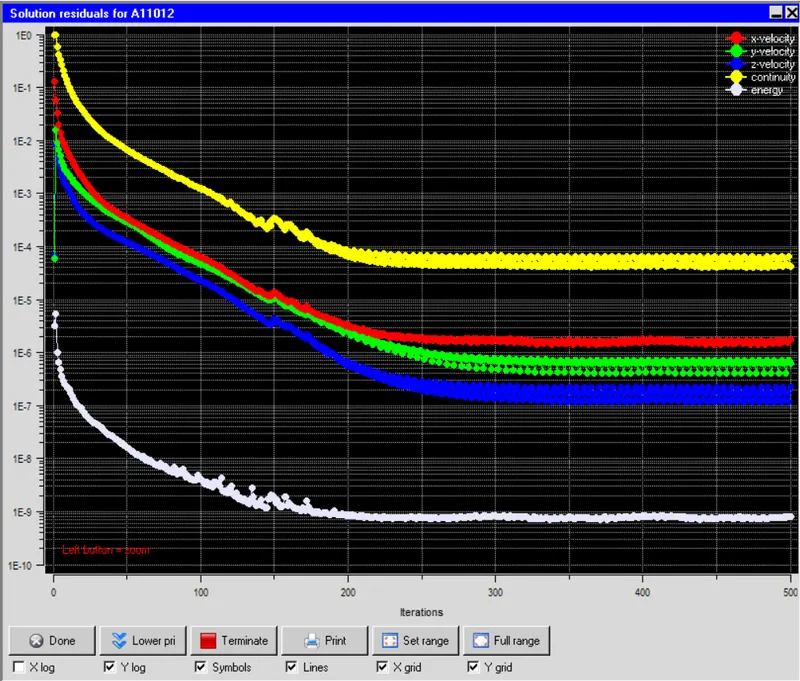
Residuals:
The residuals for the following equations are plotted against the number of iterations:
i. Continuity equation
ii. X-momentum equation
iii. Y-momentum equation
iv. Z-momentum equation
v. Energy equation
Temperature monitor:
Temperature monitor points are created within the computational domain not only to monitor the steady-state temperatures of the key objects in the model, such as heat sources and heat sinks, but also to inform the advent of steady state. The image attached below shows the data recorded by the temperature monitor points plotted against the number of iterations.
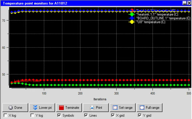
It can be seen that after 100 iterations there is no appreciable change in the recorded temperatures which indicates that the energy equation has possibly converged. According to the plot, the objects attain the following steady-state temperatures:
i. U8: 73.32 deg. C
ii. BOARD_OUTLINE.1: 73.69 deg. C
iii. heatsink.1: 47.92 deg. C
iv. heatsink.1.1: 46.21 deg. C
PCB traces:
The images attached below show the PCB-traces using different display options.
1. Single color
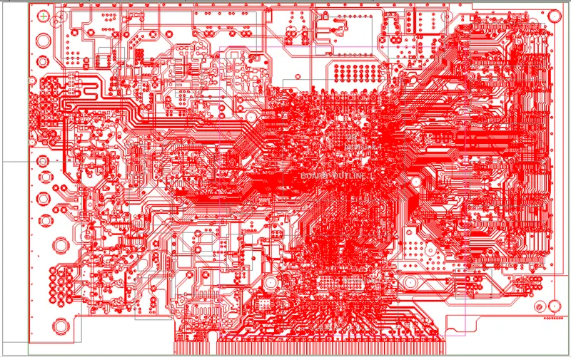
This option displays all the PCB-traces using a single color.
2. Color by trace
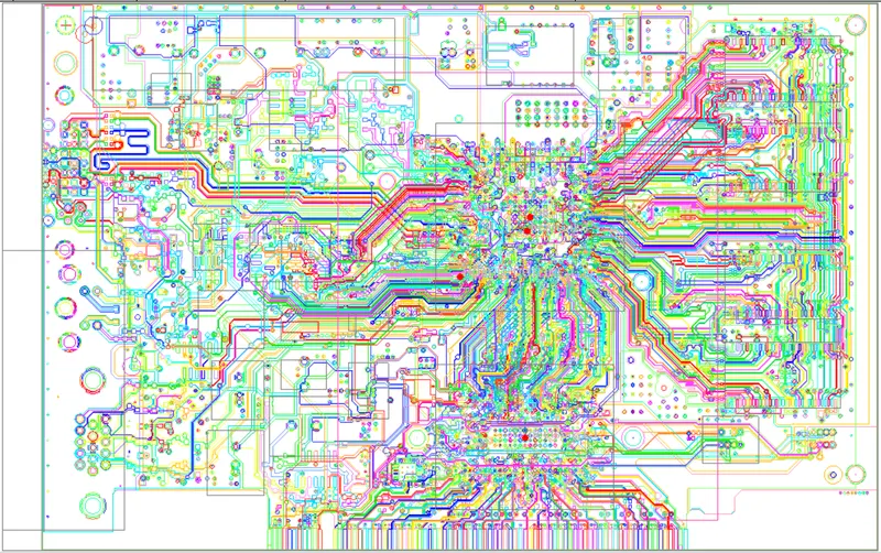
This option displays different PCB-traces using different colors.
3. Color by layer
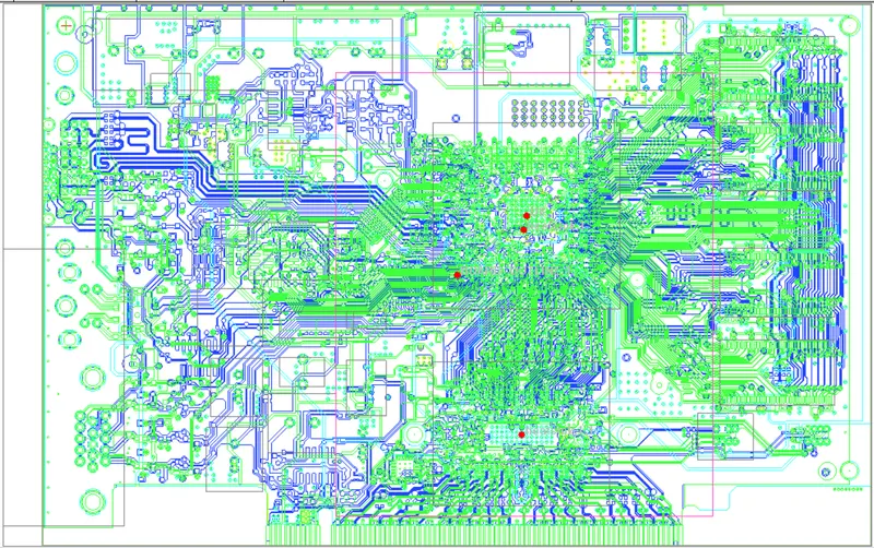
This option displays the PCB-traces in different layers using different colors.
Metal fractions:
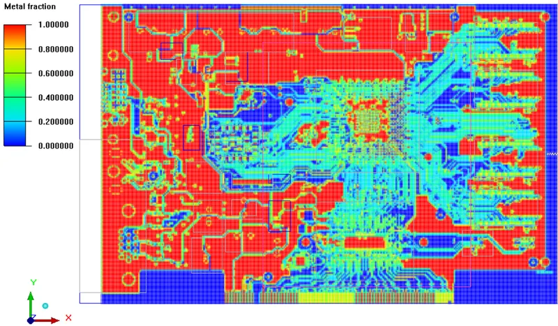
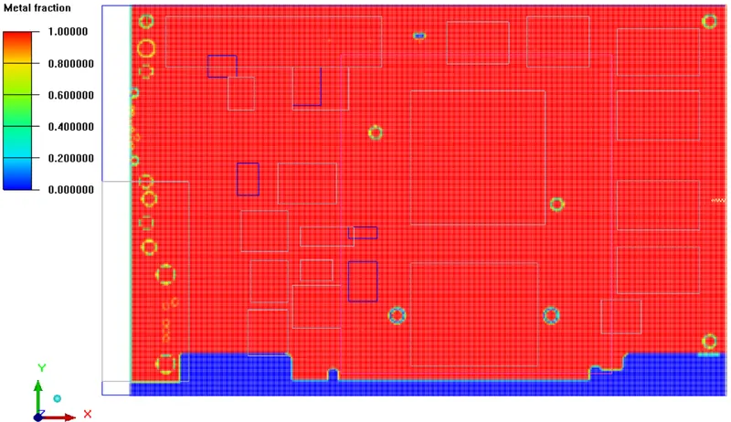
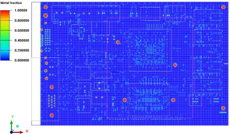
The images attached below show the metal fraction contours plotted over the different layers of the PCB.
1. Layer 1
2. Layer 2
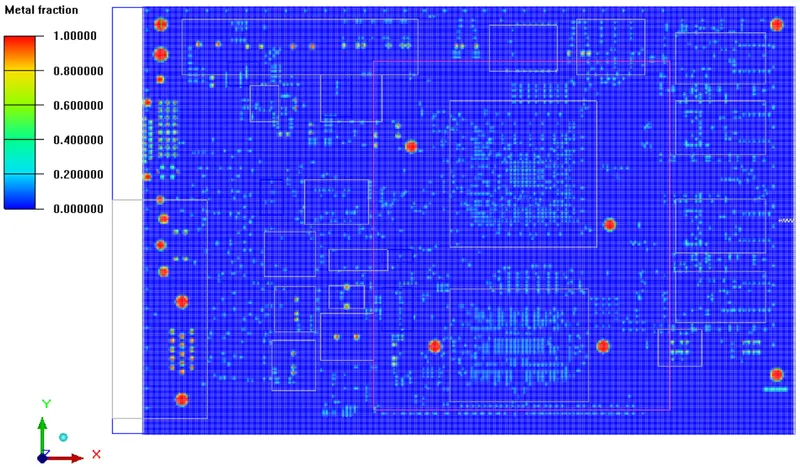
3. Layer 3
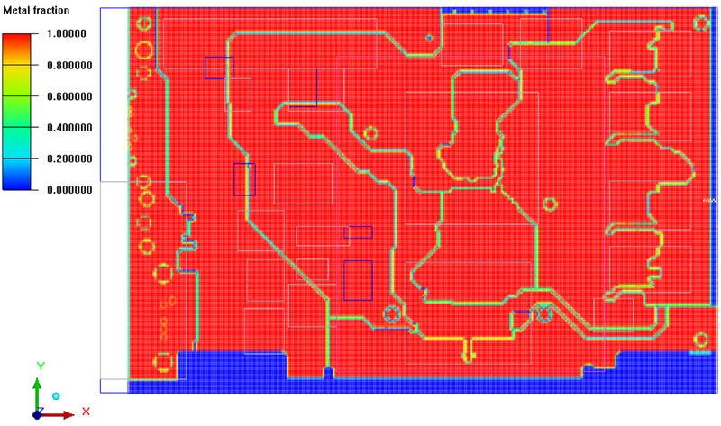
4. Layer 4
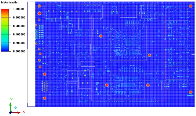
5. Layer 5
6. Layer 6
7. Layer 7
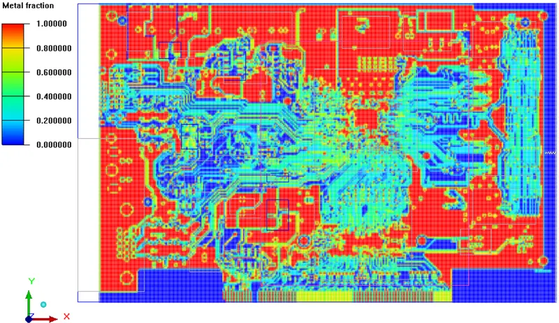
It is evident from the contours that a dielectric layer (with no copper traces) is sandwiched between two adjacent PCB layers that contain copper traces.
Thermal conductivity contours:
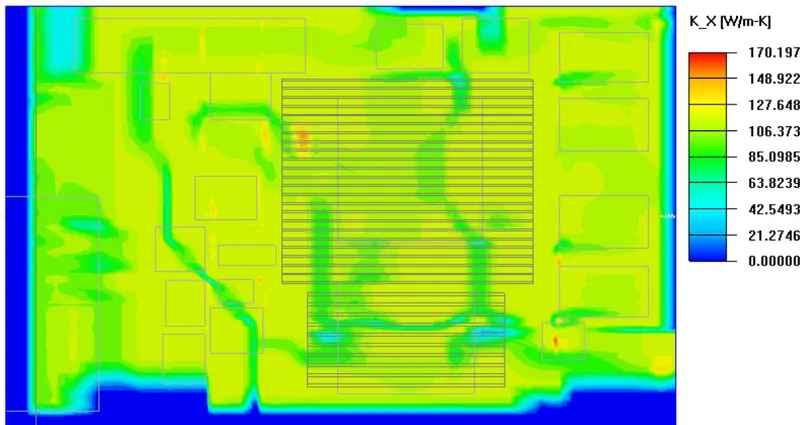
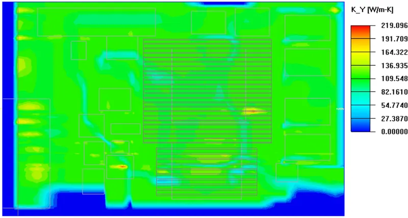
The images attached below show the kx, kY and kZ thermal conductivity contours are plotted over the Z-plane passing through the center of the PCB.
kx contours:
ky contours:
kz contours:
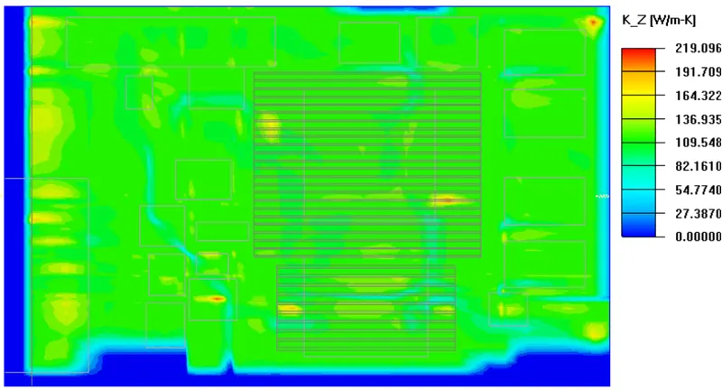
It is evident from the contours that the thermal conductivity of the PCB is anisotropic in nature.
Temperature contours:
The image attached below shows the steady-state temperature contours plotted on the Z-plane passing through the center of the PCB.
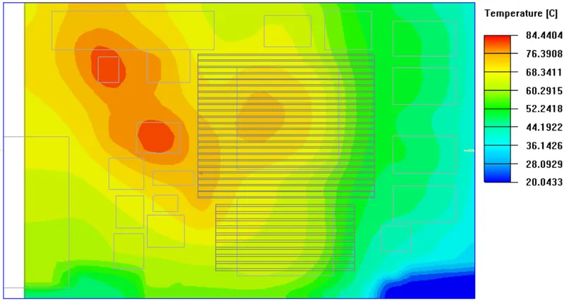
It is evident from the contour-legend that the maximum steady-state temperature on the plane is 84.44 deg. C.
Object face temperature contours:
The image attached below shows the steady-state object face temperature contours plotted on the PCB.
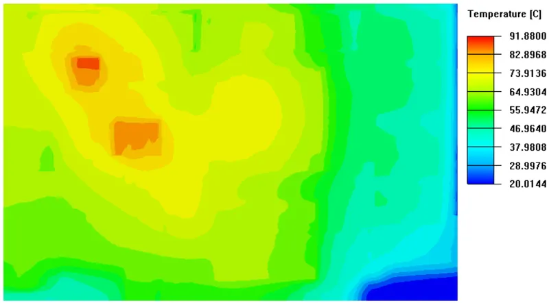
It is evident from the contours-legend that the maximum steady-state temperature on the PCB is 91.8 deg. C.
Velocity contours:
The image attached below shows the steady-state velocity contours plotted on the Z-plane passing through the center of the cabinet.
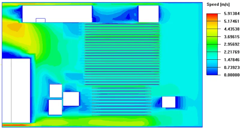
It is evident from the contour-legend that the maximum steady-state velocity on the plane is 5.91 m/s.
3.Forced convection model with trace heating:
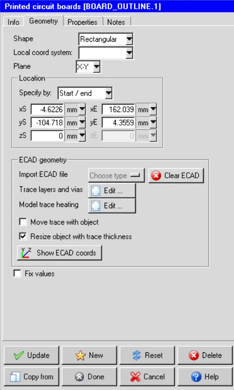
In order to model trace heating in one of the traces present in the second trace layer of the PCB, a solid trace is created out of it using the following settings in the "Trace heating" window:
i. Min area: 4124 mm^2
ii. Max angle: 135
iii. Min length: 1 m
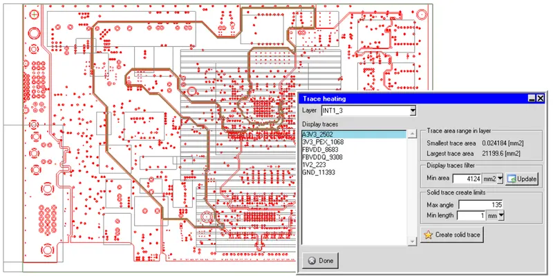
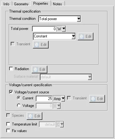
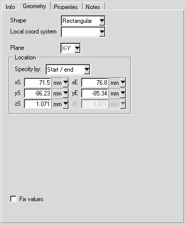
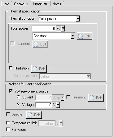
Once the solid trace is created two voltage/current type sources are created on it using the following settings:
i. Source 1
Geometry Properties
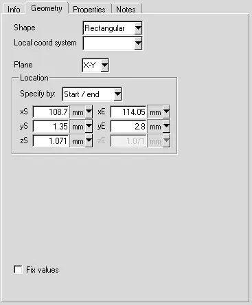
ii. Source 2
Geometry Properties
Geometry:
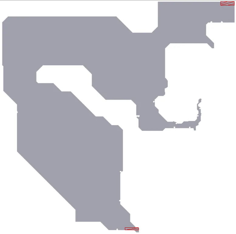
Apart from the addition of a solid trace and two voltage/current type sources, the geometry of the current model remains the same as that used for the forced convection model. The image attached below shows the solid trace and the two sources created using the settings described above.
Meshing:
A non-conformal assembly is defined around the trace to reduce the mesh count and the mesh settings applied for the forced convection model are applied again for the current model. The image attached below shows the "Mesh control" window.
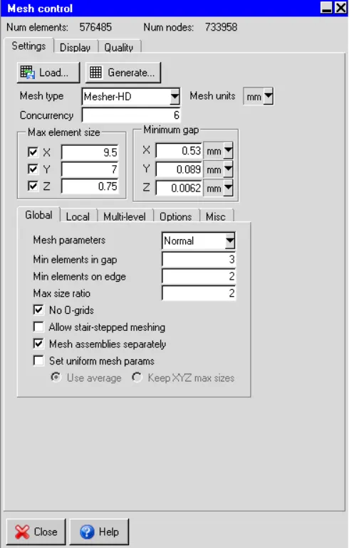
It can be seen that the mesh settings yield 576485 elements and 733958nodes. The images attached below show the computational mesh plotted on three mutually perpendicular planes, each passing through the center of the cabinet.
X-plane:

Y-plane:

Z-plane:
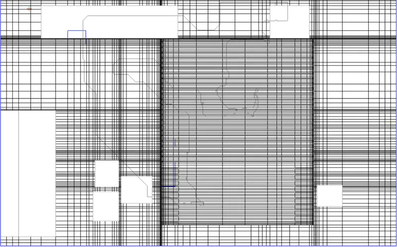
Visually the mesh appears to be fine. The images attached below show the histograms with the number of elements plotted along the X-axis and the quality measures plotted along the Y-axis.
1. Face-alignment
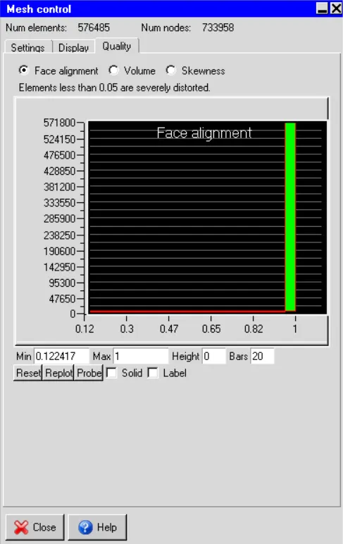
Values less than 0.05 indicate the presence of severely distorted elements in the mesh.
2. Volume
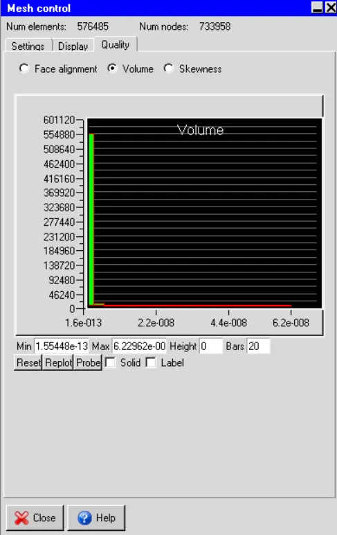
3. Skewness
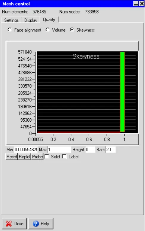
A skewness of 0 indicates that the mesh element is degenerate whereas a skewness of 1 indicates that it is ideal (equilateral/equiangular).
Solver:
The three-dimensional steady-state Navier-Stokes equations for the model are solved within the computational domain for flow and temperature field using the Fluent solver available in ANSYS Icepak. The solver-settings used for the forced convection model are reused for the solver in the current model. BCGSTAB is chosen as the stabilization criterion for both temperature and Joule heating potential.
Results:
In the current section, the simulation results are discussed.
Residuals:The residuals for the following equations are plotted against the number of iterations:
i. Continuity equation
ii. X-momentum equation
iii. Y-momentum equation
iv. Z-momentum equation
v. Energy equation
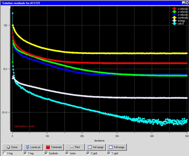
It can be seen that the residuals are quite small quantitatively and don't change appreciably between 400-500 iterations which indicates that the solution has reached a steady state. For the current model, the simulation results after 500 iterations are considered as steady-state results.
Temperature monitor:
Temperature monitor points are created within the computational domain not only to monitor the steady-state temperatures of the key objects in the model, such as heat sources and heat sinks, but also to inform the advent of steady state. The image attached below shows the data recorded by the temperature monitor points plotted against the number of iterations.
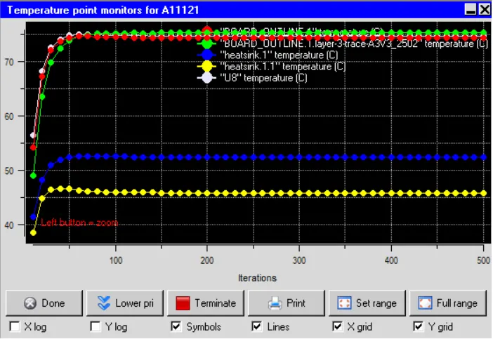
It can be seen that after 100 iterations there is no appreciable change in the recorded temperatures which indicates that the energy equation has possibly converged. According to the plot, the objects attain the following steady-state temperatures:
i. U8: 74.26 deg. C
ii. BOARD_OUTLINE.1: 74.43 deg. C
iii. heatsink.1: 53.21 deg. C
iv. heatsink.1.1: 47.38 deg. C
v. BOARD_OUTLINE.1.layer-3-trace-A3V3_2784: 75.48 deg. C
The images attached below show the PCB-traces using different display options.
2.1. Single color
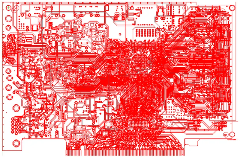
This option displays all the PCB-traces using a single color.
2.2. Color by trace
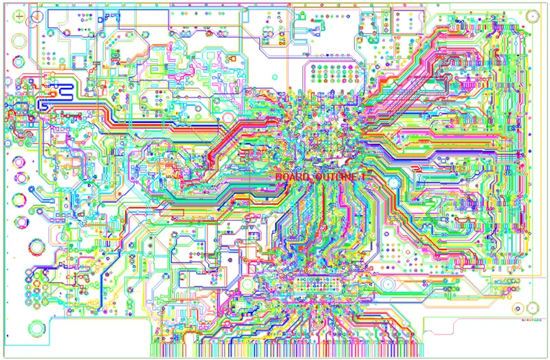
This option displays different PCB-traces using different colors.
2.3. Color by layer
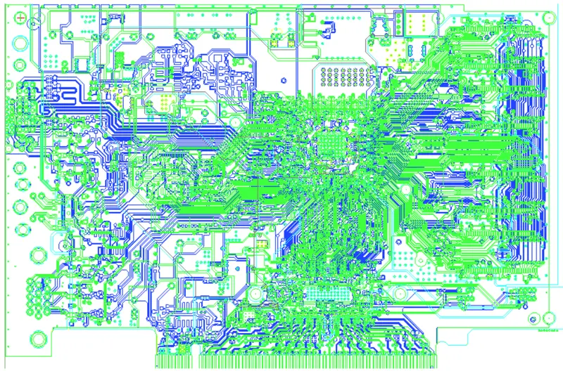
This option displays the PCB-traces in different layers using different colors.
2.4 Color by net
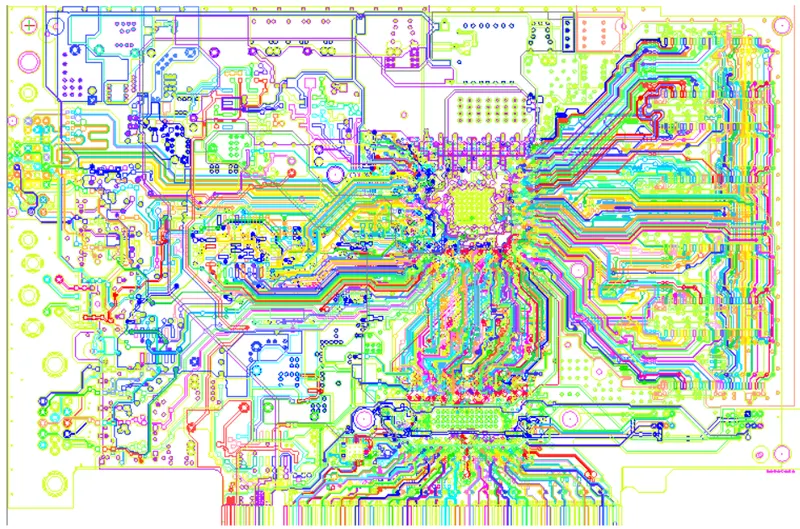
Metal fractions:
The images attached below show the metal fraction contours plotted over the different layers of the PCB.
3.1. Layer 1
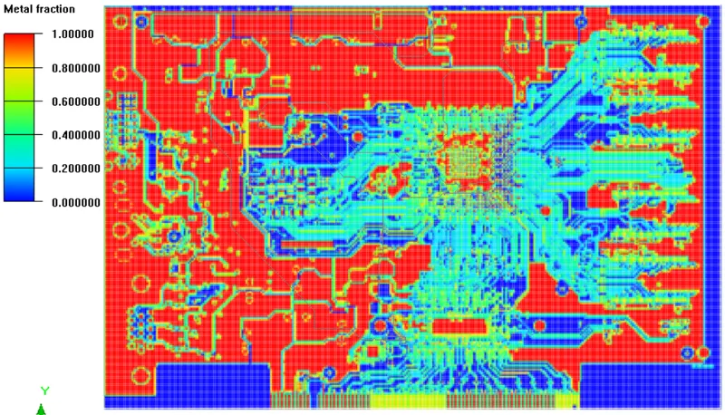
3.2. Layer 2
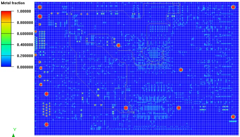
3.3. Layer 3
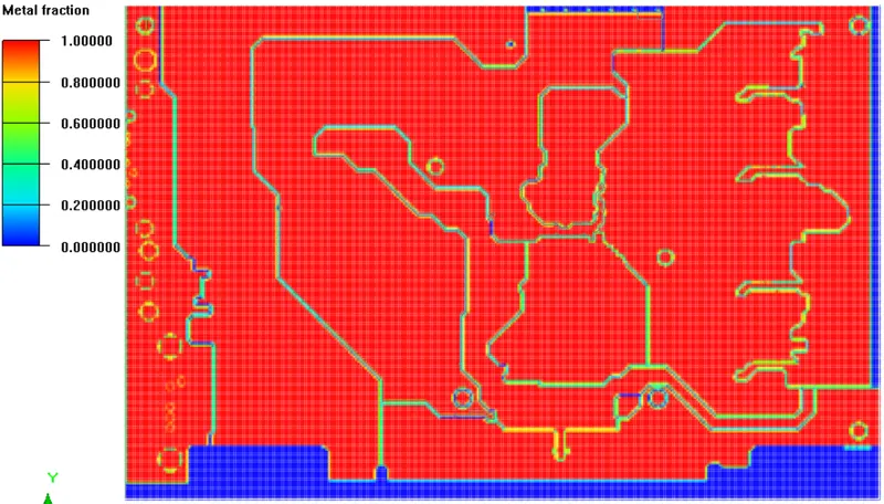
3.4. Layer 4
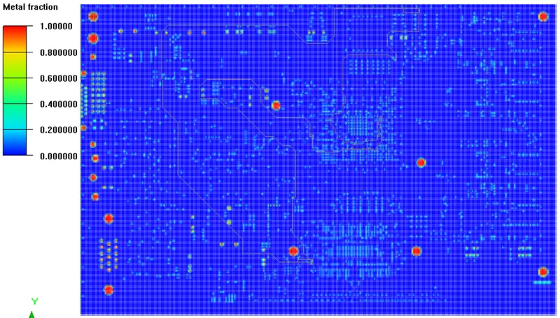
3.5. Layer 5
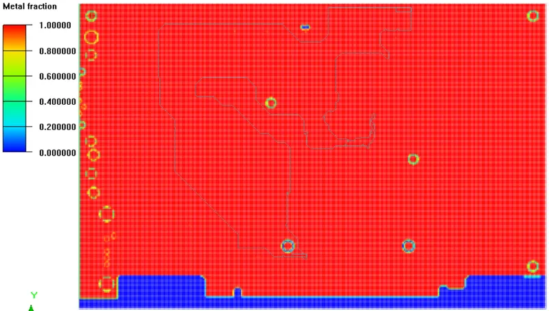
3.6. Layer 6
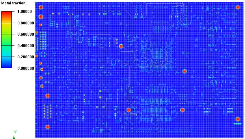
3.7. Layer 7
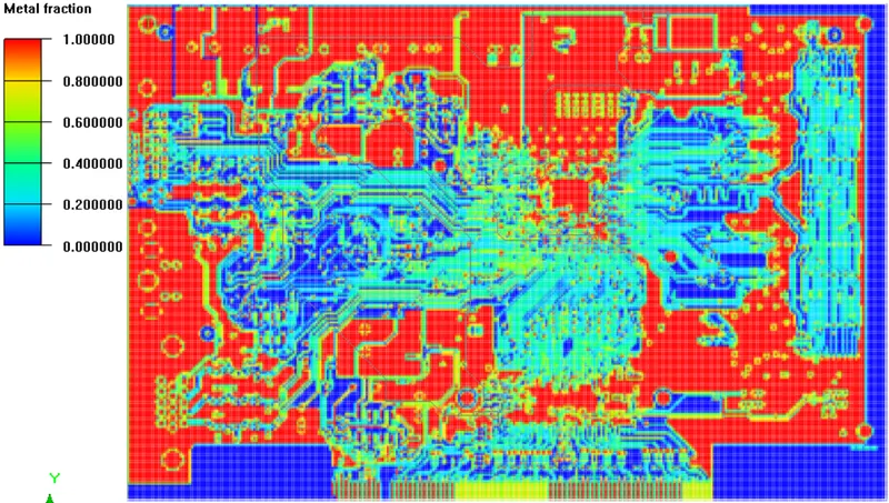
It is evident from the contours that a dielectric layer (with no copper traces) is sandwiched between two adjacent PCB layers that contain copper traces.
Thermal conductivity contours:
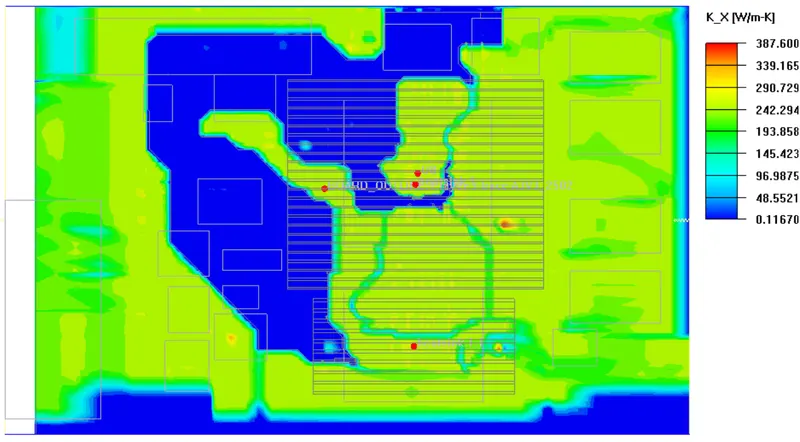
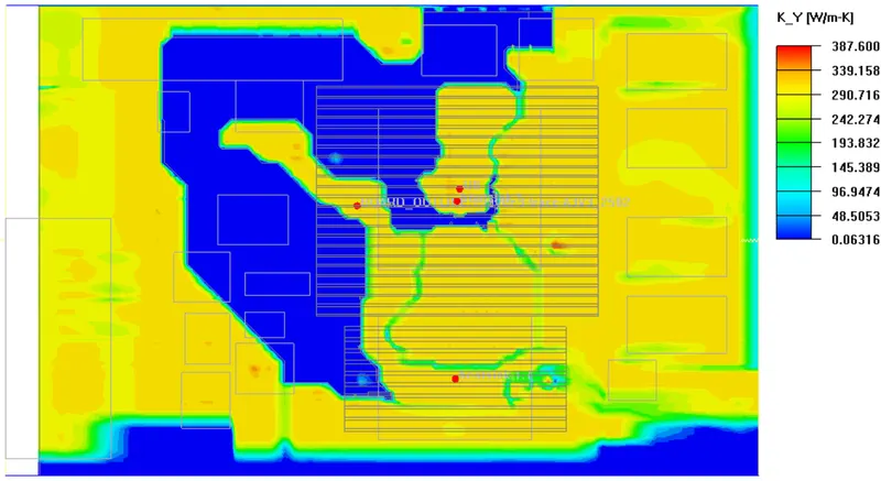
The images attached below show the kx, kY and kZ thermal conductivity contours are plotted over the Z-plane passing through the center of the PCB.
kx contours:
ky contours:
kz contours:
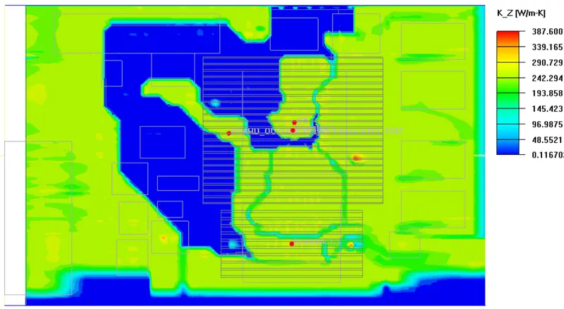
It is evident from the contours that the thermal conductivity of the PCB is anisotropic in nature.
Temperature contours:
The image attached below shows the steady-state temperature contours plotted on the Z-plane passing through the center of the PCB.
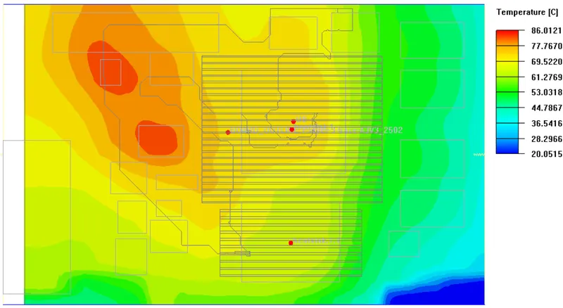
It is evident from the contour-legend that the maximum steady-state temperature on the plane is 86.01 deg. C.
Object face temperature contours:
The image attached below shows the steady-state object face temperature contours plotted on the solid trace.
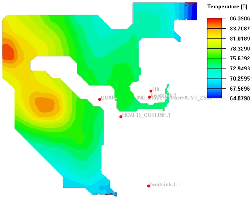
It is evident from the contour-legend that the maximum steady-state temperature on the solid trace is 86.39 deg. C
Velocity contours:
The image attached below shows the steady-state velocity contours plotted on the Z-plane passing through the center of the cabinet.
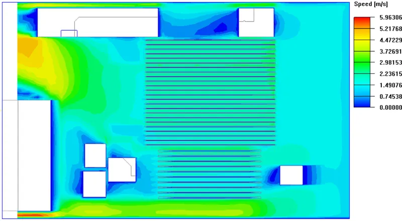
It is evident from the contour-legend that the maximum steady-state velocity on the plane is 5.96 m/s.
Electric potential contours:
The image attached below shows the steady-state electric potential contours plotted on the solid trace.
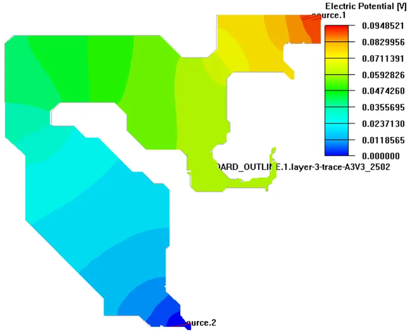
It is evident from the contour-legend that the maximum electric potential on the solid trace is 94.85 mV.
Conclusion:
In the current project, the following tasks were performed:
1. The given board file and ECAD file were imported to ANSYS Icepak.
2. All the components on the PCB were deactivated and the resulting model was solved only for conduction.
3. Key components on the PCB are activated and the resulting model was solved for forced convection.
4. In order to model trace heating, a solid trace was created using the identified trace and two voltage/current type sources were created using appropriate settings. The resulting model was solved for forced convection and trace heating.