Design and simulation of up/down converters using Simulink
1- Design a buck-boost converter with a source varying from 10 to 14 V. The output voltage is regulated at – 12 V. The load power is 15 W. The output voltage ripple must be less than 1 % for any operating condition.
a) Determine the range of the duty ratio of the switch.
b) Design the inductor and capacitor values used in your design.
c) Confirm your solutions using a simulation software for every operating condition (you must show the input voltage, the duty ratio, the output voltage “including the ripple” and the inductor current “including the ripple”).
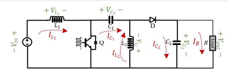
2- The Sepic DC/DC converter shown below has 𝑉𝑠=3.3 𝑣,𝐷=0.7,𝐿1=4 𝜇𝐻,𝑎𝑛𝑑 𝐿2=10 𝜇𝐻,𝐶1=𝐶2=50𝜇𝐹. The load resistor is 5 Ω, and 𝑓𝑠=300 𝑘𝐻𝑧.
a) Determine the maximum and the minimum values of the inductor currents in 𝐿1 and 𝐿2.
b) Determine the variation in the capacitor voltages in both 𝐶1 and 𝐶2.
c) Confirm your results using a simulation software package.
Your Answers
1- Design a buck-boost converter with a source varying from 10 to 14 V. The output voltage is regulated at – 12 V. The load power is 15 W. The output voltage ripple must be less than 1 % for any operating condition.
a) Determine the range of the duty ratio of the switch.
b) Design the inductor and capacitor values used in your design.
c) Confirm your solutions using simulation software for every operating condition (you must show the input voltage, the duty ratio, the output voltage “including the ripple” and the inductor current “including the ripple”).
Solution:
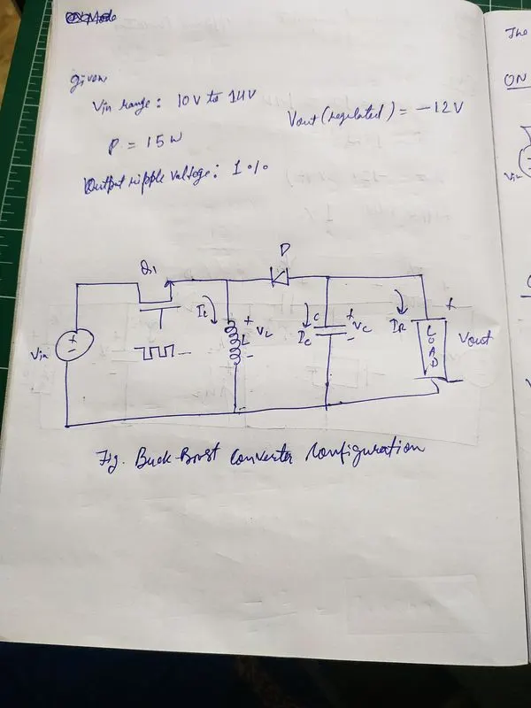
To Design buck-boost converter
Given Data,
Vin range: 10V to 14V
Power: 15W
Vout: -12V
Output Voltage Rippel: 1%
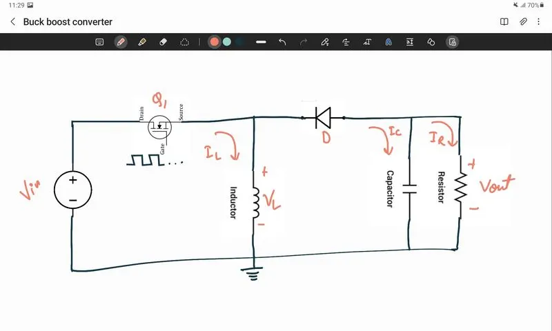
Schematic Diagram:
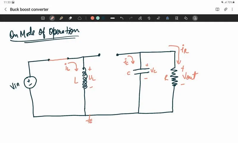
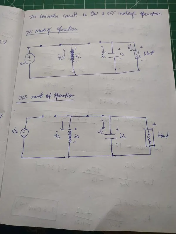
On the mode of operation:
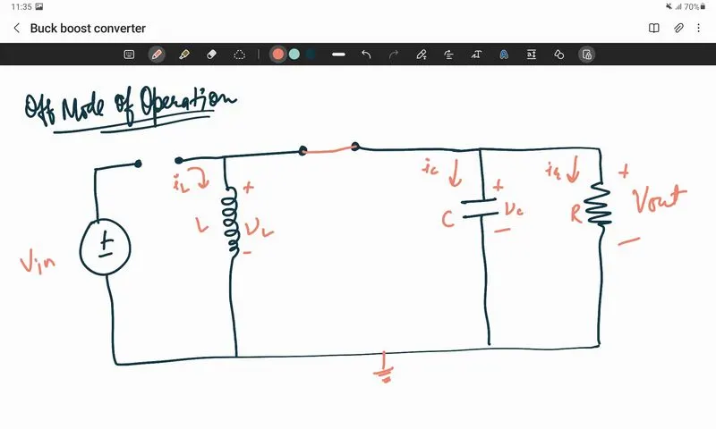
Off mode of operation:
Calculation:
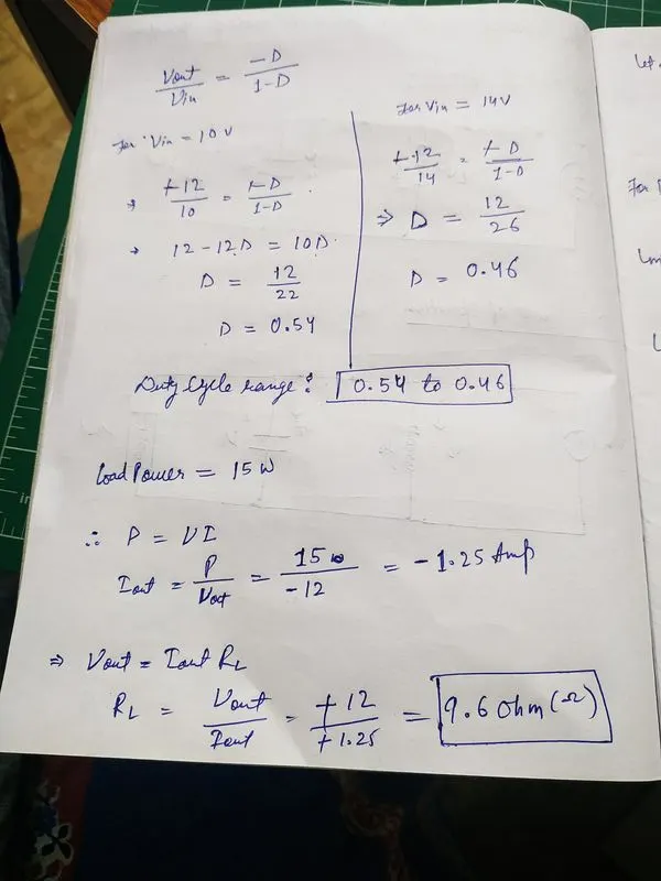
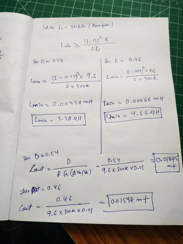
as per the calculation,
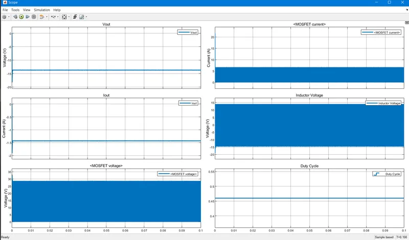
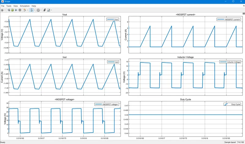
Duty Cycle range: 0.54 to 0.46
R(Load)= 9.6 Ohm
Lmin (D: 0.54)= 3.38uH
Lmin (D: 0.46)= 4.66uH
Cout (D: 0.54)= 18.75uf
Cout (D: 0.46)=15.97uf
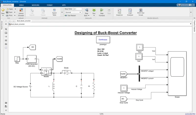
Matlab Circuit Diagram:
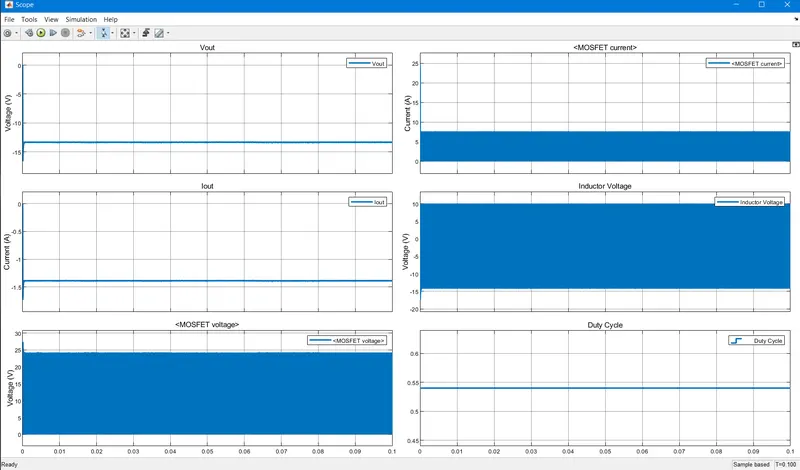
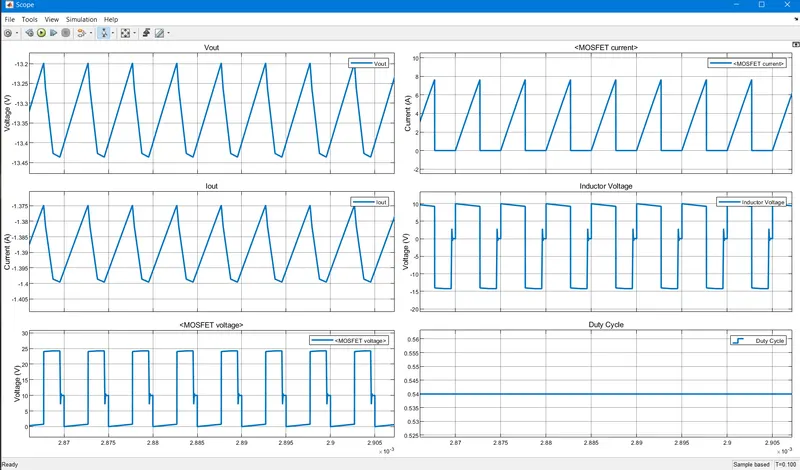
Output Waveform of the input voltage, the duty ratio, the output voltage “including the ripple” and the inductor current “including the ripple”
For,
Vin= 10V
Duty Cycle= 0.54
Lmin= 3.38uH
Cout= 18.75uf
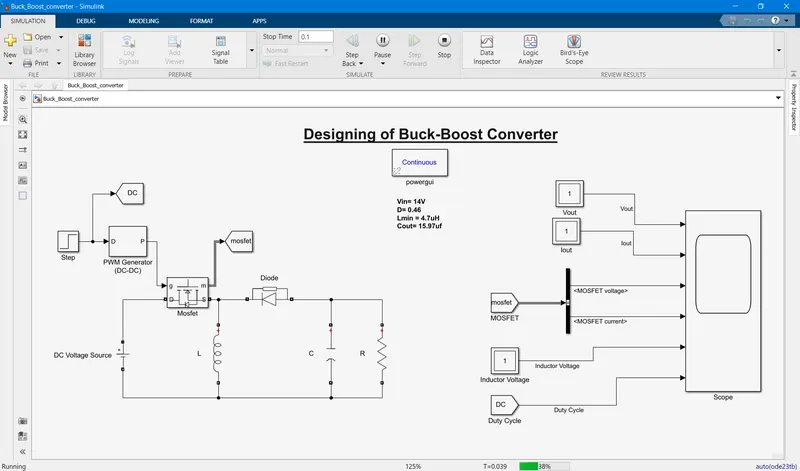
Circuit Diagram for,
Vin= 14V
Duty Cycle= 0.46
Lmin = 4.66uH
Cout = 15.97uf
Output Waveform of the input voltage, the duty ratio, the output voltage “including the ripple” and the inductor current “including the ripple”
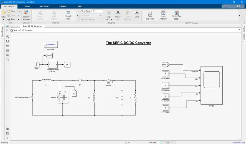
2- The Sepic DC/DC converter shown below has 𝑉𝑠=3.3 𝑣,𝐷=0.7,𝐿1=4 𝜇𝐻,𝑎𝑛𝑑 𝐿2=10 𝜇𝐻,𝐶1=𝐶2=50𝜇𝐹. The load resistor is 5 Ω and 𝑓𝑠=300 𝑘𝐻𝑧.
a) Determine the maximum and the minimum values of the inductor currents in 𝐿1 and 𝐿2.
b) Determine the variation in the capacitor voltages in both 𝐶1 and 𝐶2.
c) Confirm your results using a simulation software package.
Simulation:
Matlab Circuit Diagram:
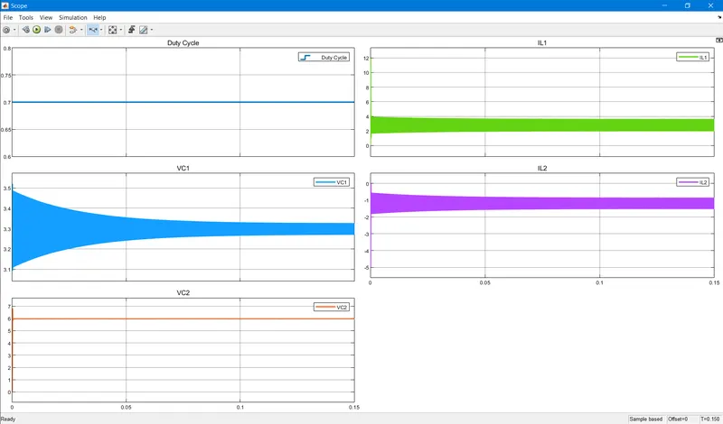
Output Waveform of
Voltage Across C1 & C2
Current Through L1 & L2
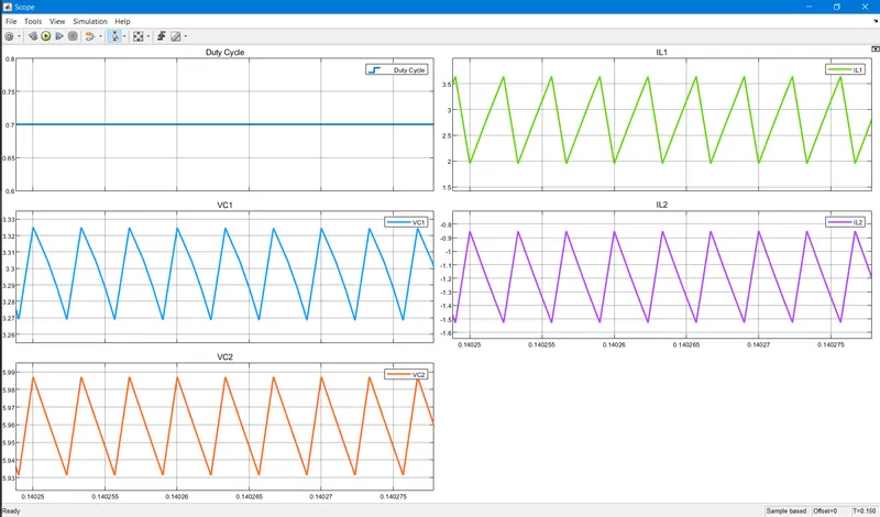
Comments:
a) Determine the maximum and the minimum values of the inductor currents in 𝐿1 and 𝐿2.
- The maximum value of the inductor current in 𝐿1: 3.5A
-
The minimum value of the inductor current in 𝐿1: 2.0A
-
The maximum value of the inductor current in 𝐿2: -0.9A
-
The minimum value of the inductor current in 𝐿2: -1.5A
b) Determine the variation in the capacitor voltages in both 𝐶1 and 𝐶2.
- The maximum value of the capacitor voltages in 𝐶1: 3.32V
-
The minimum value of the capacitor voltages in 𝐶1: 3.27V
-
The maximum value of the capacitor voltages in 𝐶2: 5.98V
-
The minimum value of the capacitor voltages in 𝐶2: 5.93V
Hence, All the Data is verified from the simulation.
---------------------------------------------------------------------------------------------------------------------------------------------------------------------------------------------------------------------------END-------------------------------------------------------------------------------------------------------------------------------------------------------------------------------------------------------------------------------