To design a double sided USB type C to RJ45 ethernet interface PCB utilizing bus-powered following the length matching of the high speed signals and EMC/EMI complaint.
Project on PCB Design:
To design a double-sided USB type C to RJ45 ethernet interface PCB utilizing bus-powered
following the length matching of the high-speed signals and EMC/EMI complaint.
Challenge:
- Creating a workspace for LAN7800 in Altium
- Defining a PCB board size using the DXF data provided
- PCB clearance to be set as 0.15mm and track width to be 0.2mm for power line and
0.15mm for the rest of the circuit
- Following the block diagram provided for creating the schematic and using the datasheet
for creating the footprint and symbol.
- Use Saturn PCB tool to find the values for 100ohm impedance for the high speed
differential pair signals
- Set PCB to 4 layers following the board stack-up provided
- Identifying the key points to consider for PCB design using the datasheet
- Assemble and route the components as recommended by the datasheet
- Place the components on both sides of the PCB and tracking on both sides.
- Add 2 fiducials diagonally opposite
- PCB board with the text (“Ethernet Interface”)
- Generate 3D files for all the components and a 3D view.
- Generate PCB panel of 150mm x 150mm and place as many circuits as possible and
follow routed method using mouse bites
- Generate complete output files for DFM and DFA (Gerber, Altium draftsman, X Y data,
BOM, assembly diagram, fabrication diagram)
Your Answers
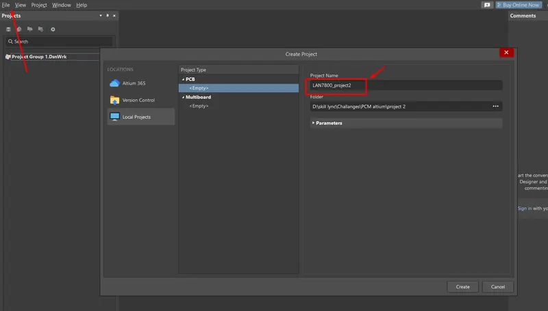
- Creating a workspace for LAN7800 in Altium
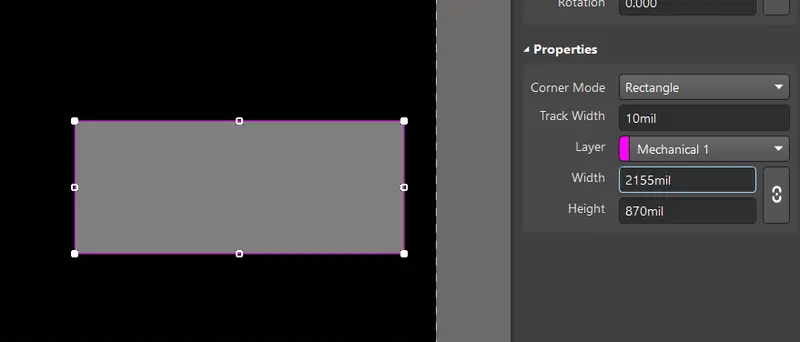
- Defining a PCB board size using the DXF data provided
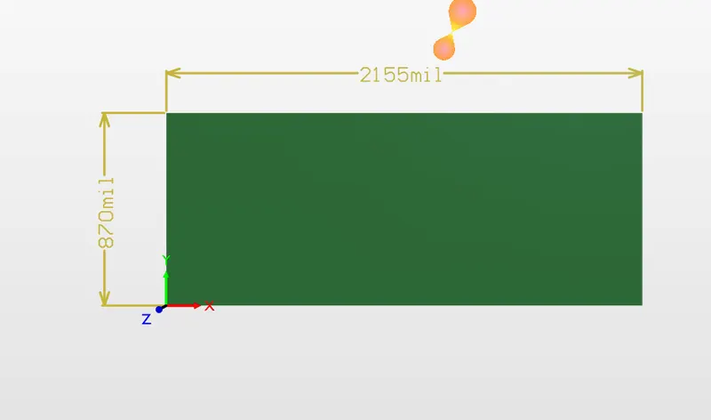
PCB board size (in mils) : 2155x870
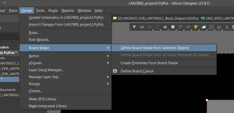
To make Board shape as a required dimension: Go to Design>> Board shape>> Define Board Shape From Selected Object after creating the outline of the required dimension of 2155x870 mil
- PCB clearance to be set as 0.15mm and track width to be 0.2mm for power line and
For clearance rules set: go to Design>> Rules>> Clearance
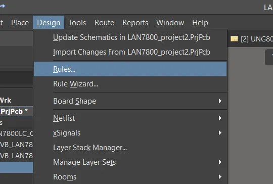
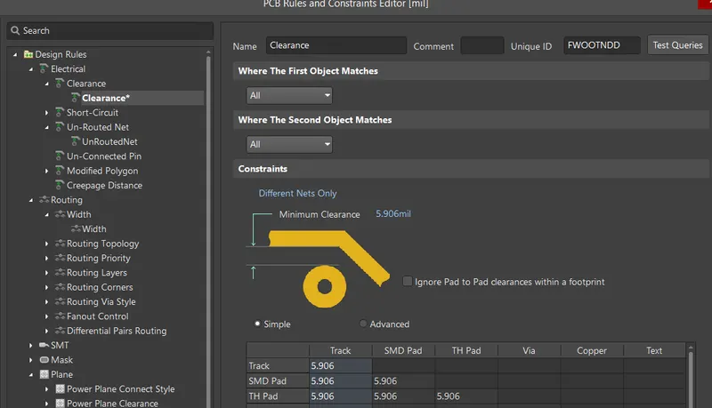
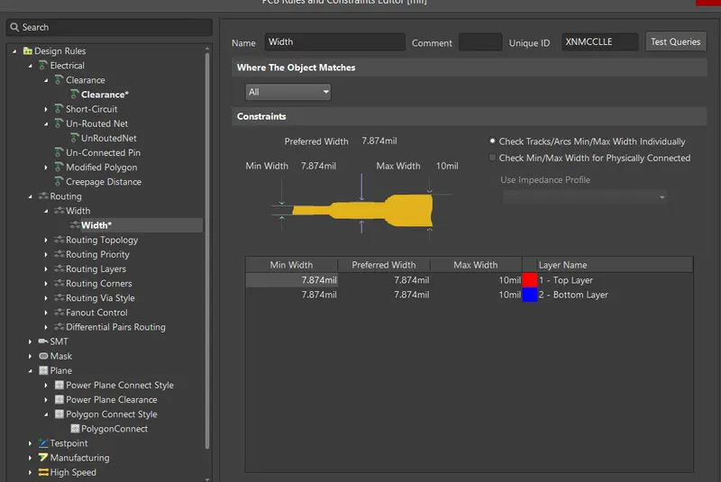
- Following the block diagram provided for creating the schematic and using the datasheet for creating the footprint and symbol.
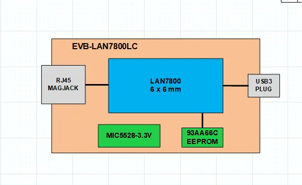
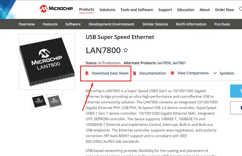
with the help of the data provided.
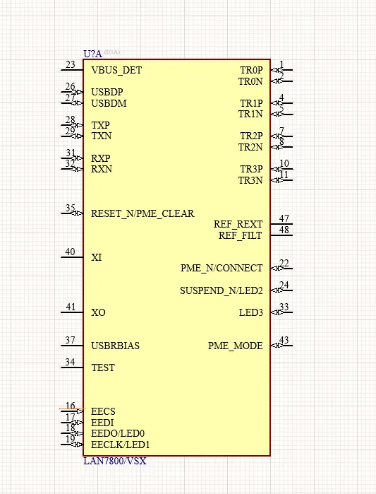
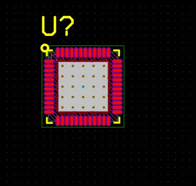
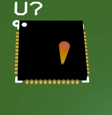
- Use Saturn PCB tool to find the values for 100ohm impedance for the high speed
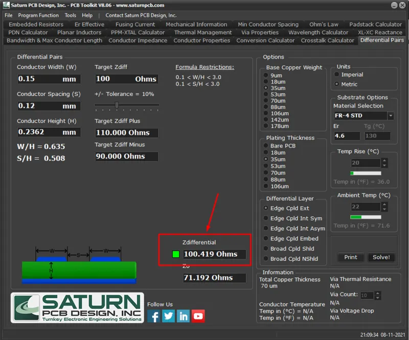
- Set PCB to 4 layers following the board stack-up provided
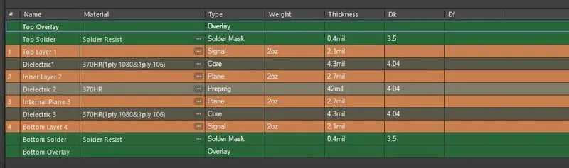
- Add 2 fiducials diagonally opposite

- Generate 3D files for all the components and a 3D view.
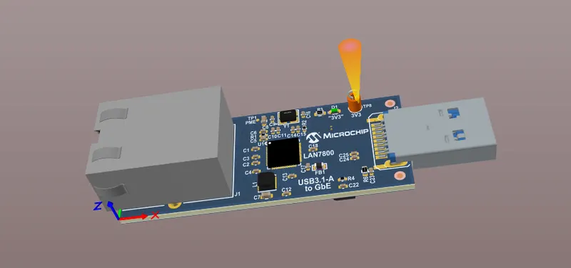
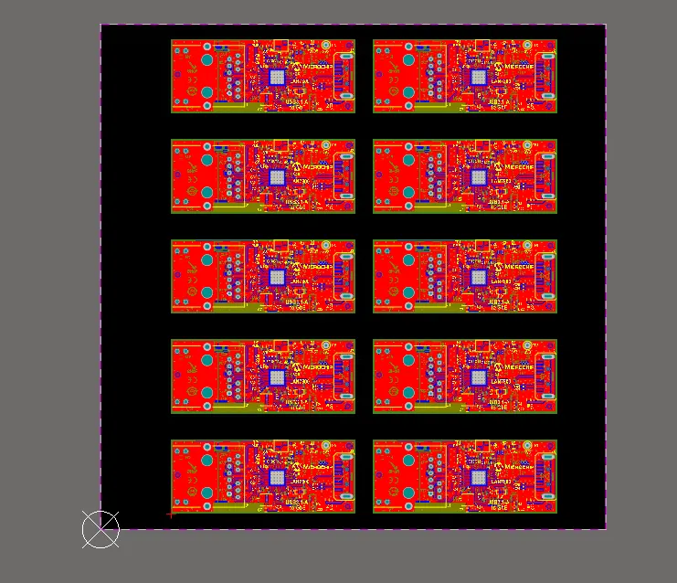
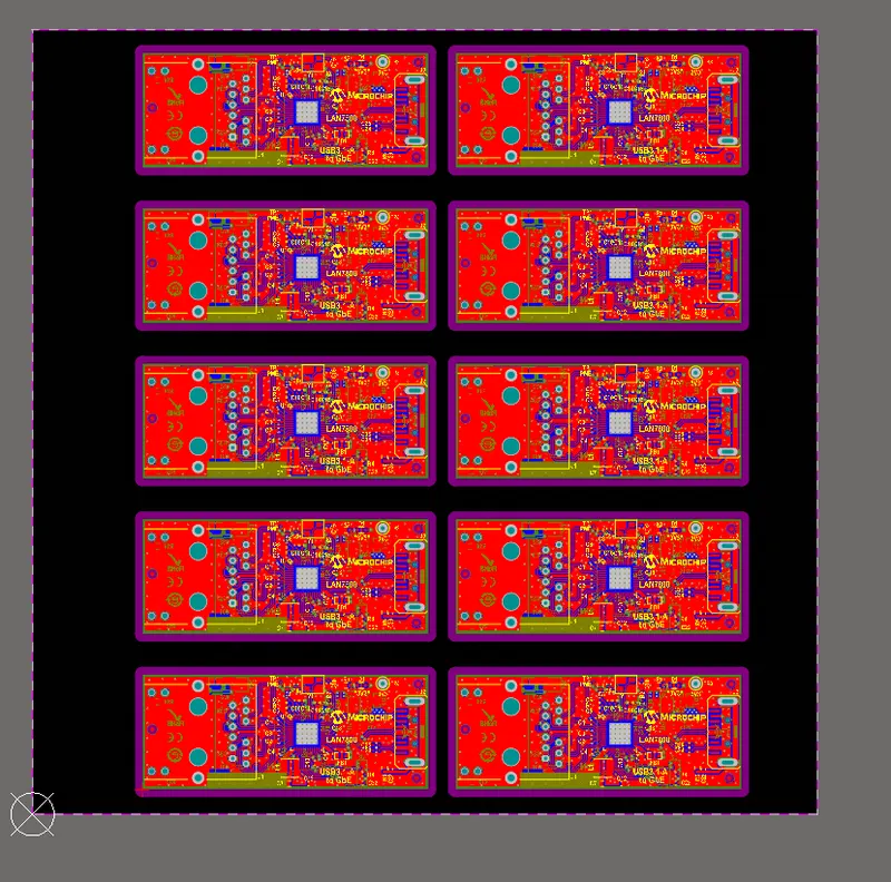
- Generate PCB panel of 150mm x 150mm and place as many circuits as possible and
follow routed method using mouse bites
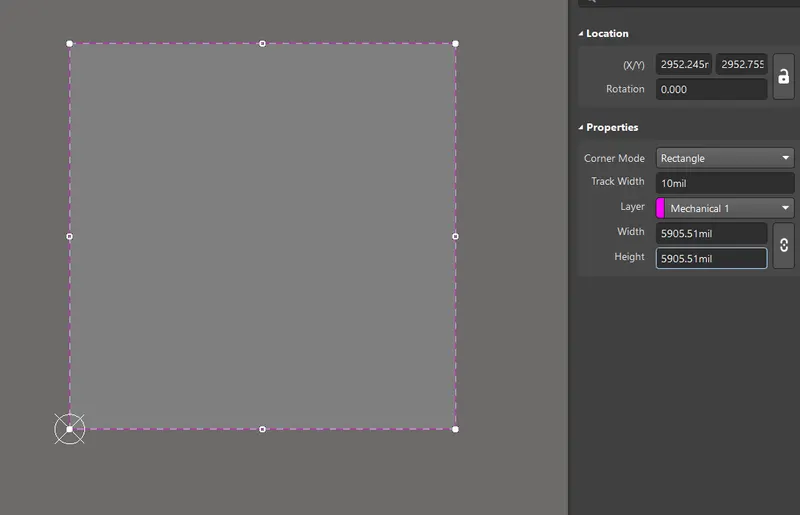
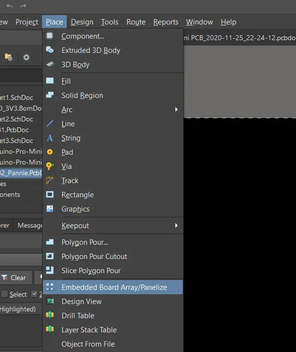
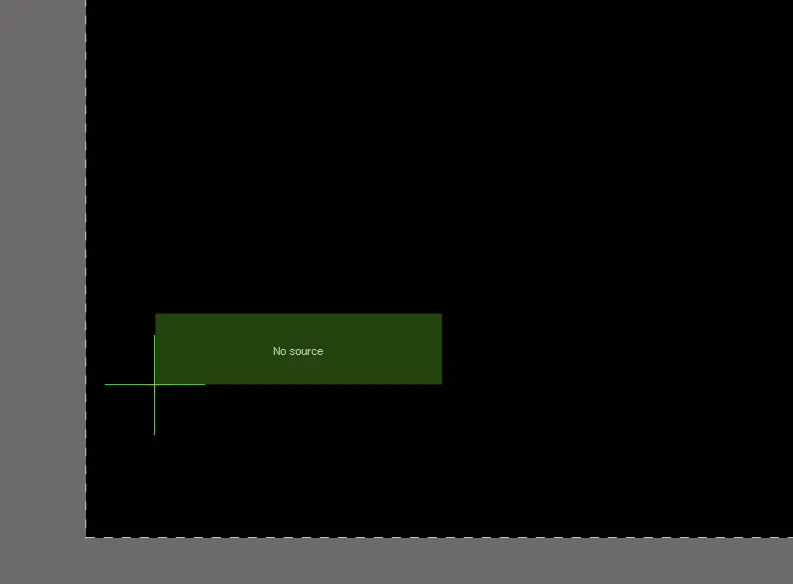
after creating the 150mmx150mm board go to Place>> Embedded Board array
Panel created:
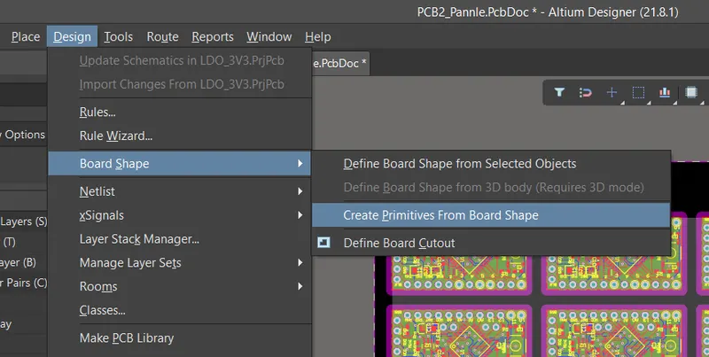
now go to Design>> Board Shape>> Create Primitives from board shape
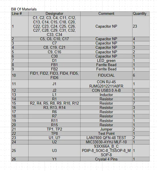
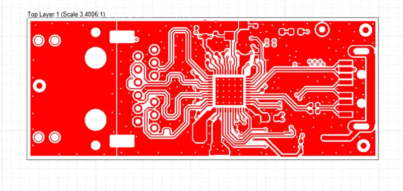
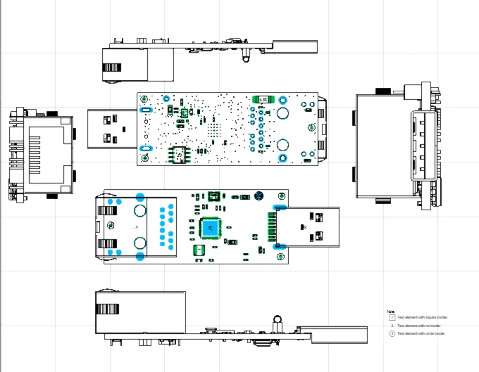
- Generate complete output files for DFM and DFA (Gerber, Altium draftsman, X Y data,
BOM, assembly diagram, fabrication diagram)
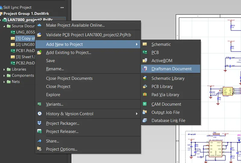
Altium draftsman