Power Electronics
Power Electronics is a technology that deals with the conversion and control of electrical power with the help of power semiconductor devices that operate in switching mode.
Governing Equations:
Power loss = V*I
Ideal Case:
Power electronics devices behave like switches,
When the switch is open:
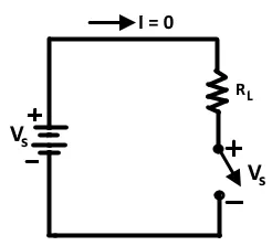
there is no current flow, and P=V*I = V*0 = 0W
When the switch is closed:
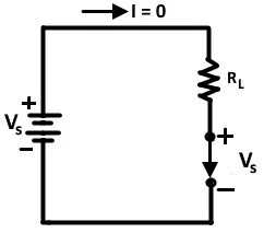
there is no voltage drop across the switch, and P=V*I = 0*I = 0W
An ideal switch implies zero loss, thus offering 100% efficiency.
Real Case:
Power losses in transistor:-
Conduction loss:
When the transistor is off, it carries a leakage current and the power loss associated with this is
Where
Vs is the voltage supply
Ileak is the leakage current
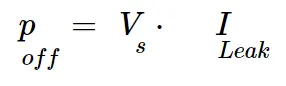
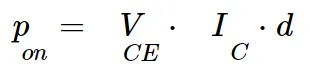
To control the power, the transistor is switched on and off in a periodic manner, hence to find the voltage power loss the duty cycle must also be considered.
Vce is the voltage between the collector and the emitter region]
d is the duty cycle = on-time/on-time+off-time
Switching loss:
In addition to conduction loss, a real switch has switching losses because it cannot change from on state to off state instantaneously. A finite time is taken to turn on and off.
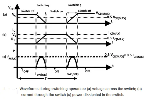
Plot(c) shows the power loss when switching from on to off state and vice-versa.
Max power loss when switching from the Off to On state is :

2.
AIM: The aim of this challenge is to use a suitable MATLAB modelm and show how duty cycle control signal can be generated for a simple power converter circuit.
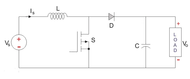
A Boost Circuit was used as a power converter circuit to show how duty cycle control signal can be generated .
CIRCUIT DIAGRAM:
Circuit Working:
The Boost converter circuit comprises of the following components:
Voltage source
Inductor
Mosfet
Diode
Capacitor
Load
When the voltage supply is on and the mosfet acts as a closed switch, current flows in the following manner:
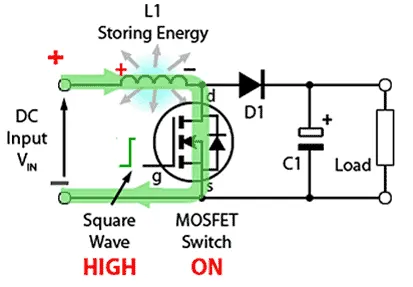
During this, the inductor gets charged and develops a magnetic field around it. There is virtually no current flowing in the remainder of the circuit as the combination of D1, C1 and the load represent a much higher impedance than the path directly through the heavily conducting MOSFET.
When the voltage supply is on and the mosfet acts as a open switch, current flows in the following manner:
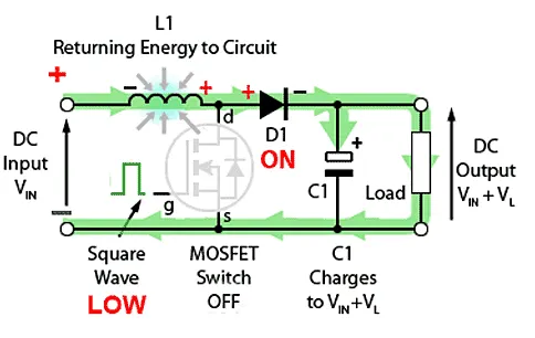
During this, the polarity of the inductor is reversed, and it slowly disipates the energy stored in the form of current. This results in two voltages, the supply voltage VIN and the back e.m.f.(VL) across L1 in series with each other.
The resulting current through D1 charges up C1 to VIN +VL minus the small forward voltage drop across D1, and also supplies the load.
When the voltage supply is on and the mosfet acts as a closed switch, current flows in the following manner:
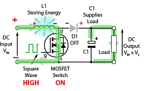
The Forward biased diode prevents the current discharged from the capacitor to flow towards the inductor, hence supplying to the load when then MOSFET is conducting. The load continues to be supplied with VIN +VL from the charge on C1.
The charge C1 drains away through the load during this period and is recharged each time the MOSFET switches off, so maintaining an almost steady output voltage across the load.
This way, a DC input voltage can be stepped up to a higher voltage with the help of a simple circuit.
MATLAB Model:
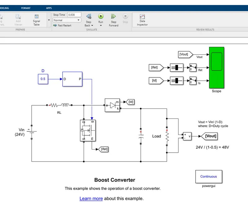
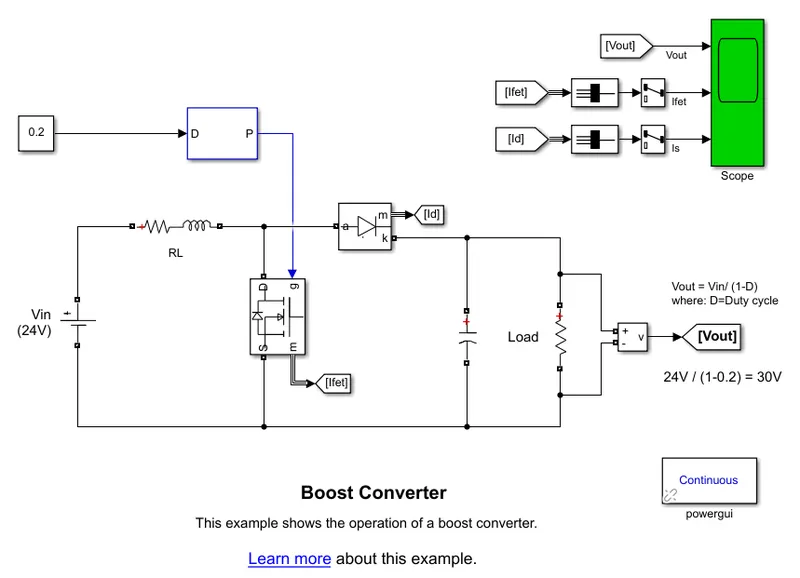
The circuit comprises of a DC voltage source of 24V, an LR branch in series, a MOSFET regulated by a duty cycle, a forward biased diode, and a capacitor and load in parallel.
The run time of the program is set to 0.008seconds.
RL series branch:
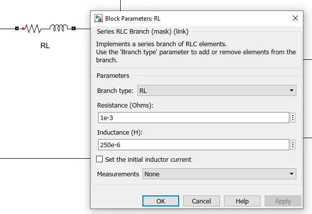
Resistance: 1e-3 Ohms
Inductance: 250e-6 Henry
Duty cycle switching frequency:
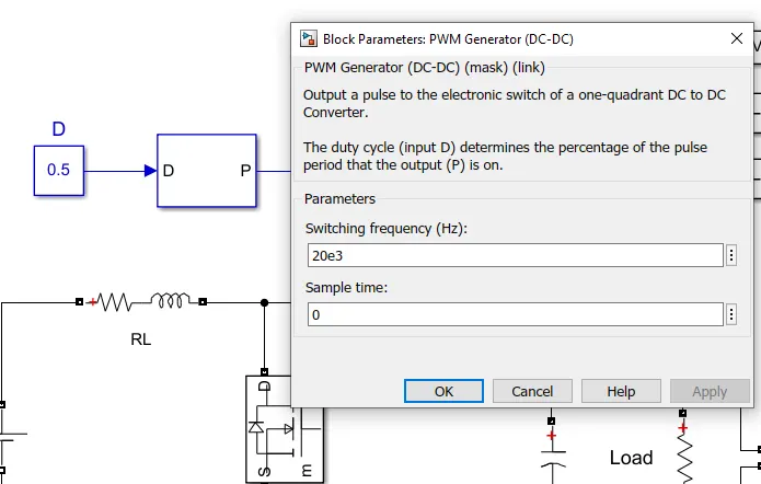
D is the duty cycle
P is the output pulse
The switching frequency was set to 20,000Hz, it is the frequency of the internal sawtooth signal used to generate the pulse.
Capacitor:
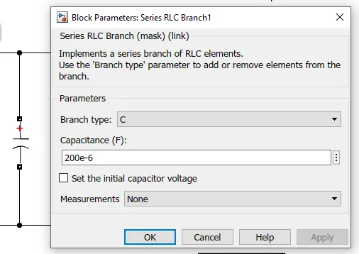
A capacitor was added to the circuit using a Series RLC branch block, and branch type was set as capacitor.
Output Voltage:
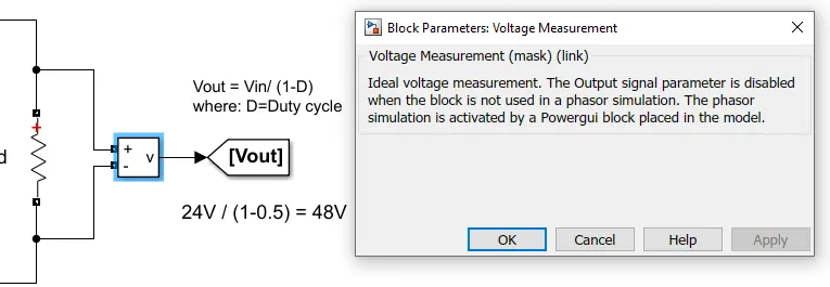
A voltage measurement block was used to measure the voltage across the load.
Output Voltage Formula:
Vout= Vin/(1-duty cycle)
Output Plot:
The first plot shows the output voltage vs time.
The second plot shows the mosfet current vs time.
The third plot shows the diode current vs time.
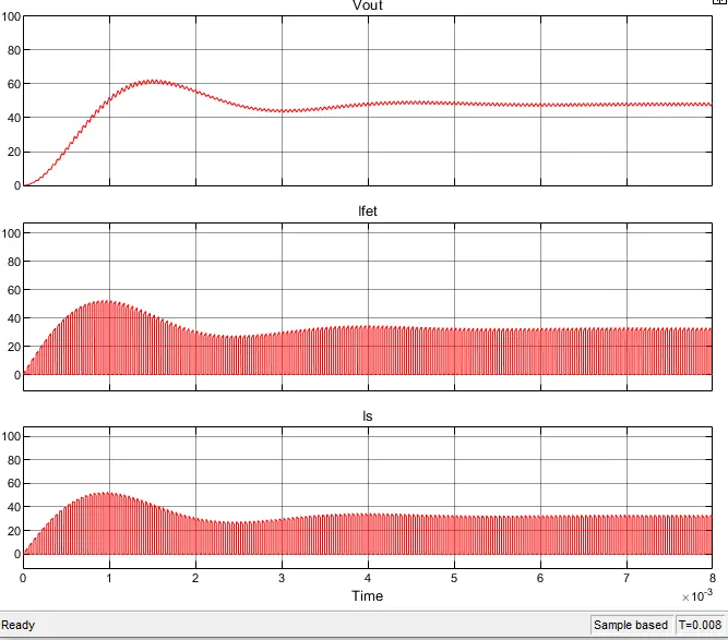
With an input voltage of 24V, we were able to obtain an output voltage of 48V.
The duty cycle ratio(On-Time/Total-time) was changed to 0.2, and the output voltage obtained was
Vout = Vin/(1-0.5) = 24/0.5 = 48V
Modified MATLAB Model:
Case 1: Duty cycle= 0.2
Output Plot:
The first plot shows the output voltage vs time.
The second plot shows the mosfet current vs time.
The third plot shows the diode current vs time.
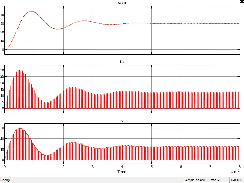
The duty cycle ratio(On-Time/Total-time) was changed to 0.2, and the output voltage obtained was
Vout = Vin/(1-0.2) = 24/0.8 = 30V
Case 2: Duty Cycle= 0.7
Output Plot:
The first plot shows the output voltage vs time.
The second plot shows the mosfet current vs time.
The third plot shows the diode current vs time.
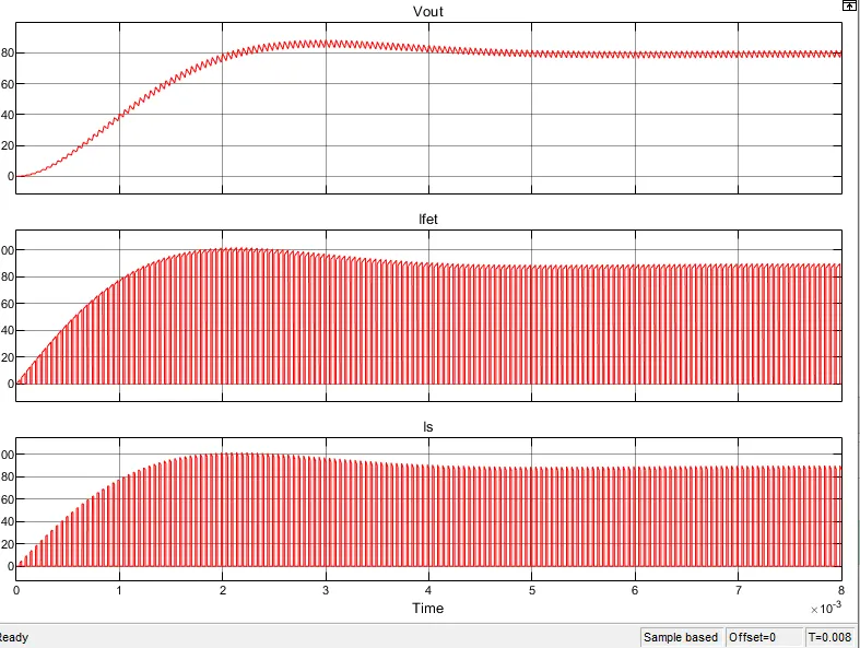
The duty cycle ratio(On-Time/Total-time) was changed to 0.2, and the output voltage obtained was
Vout = Vin/(1-0.7) = 24/0.3 = 80V
Case 3: Duty cycle = 0.6
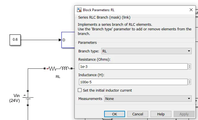
In order to reduce the fluctuation observed in the starting time, ihe inductance value was increased to 100e-5Henry
Output Plot:
The first plot shows the output voltage vs time.
The second plot shows the mosfet current vs time.
The third plot shows the diode current vs time.
A more stable output voltage was obtained in comparison to the previous circuits.
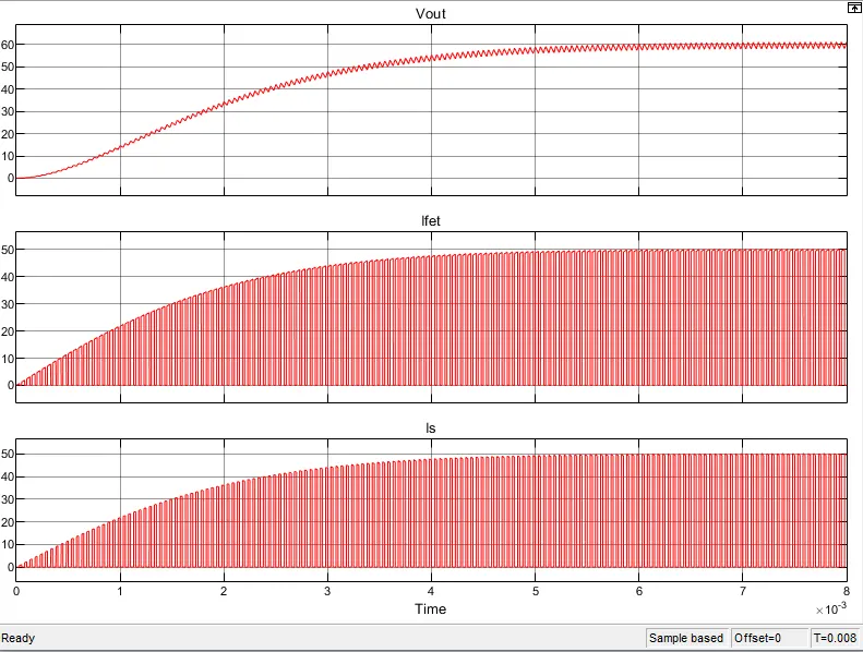
The duty cycle ratio(On-Time/Total-time) was changed to 0.2, and the output voltage obtained was
Vout = Vin/(1-0.6) = 24/0.4 = 60V
3.
An inverter is an electronic device that converts direct current(DC) to alternating current(AC).
Square Wave Inverter Voltage:
Circuit diagram:
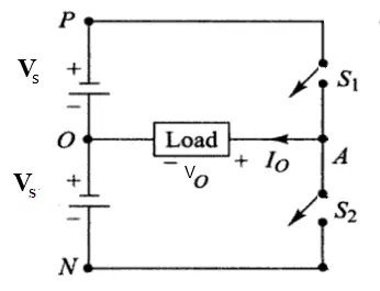
Vs is the supply voltage
V0 is the voltage across the load
S1 and S2 are the switches
When S1 is closed and S2 is open, current flows from the supply to A and across the load and back to the source.
When S2 is closed and S1 is open, current flows from the supply to O and across the load and back to the source. This time the voltage across the load is opposite to the previous case. Hence a negative voltage drop is obtained.
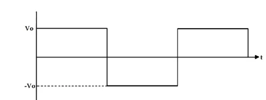
Output:
A square wave output is obtained from the DC supply.
Disadvantages of using a Square Wave Rectifier:
- Square wave voltage contains a large number of high harmonics, with iron core inductance or transformer load with electrical equipment will produce an additional loss.
- Square wave inverters are less reliable and also unsafe to use for appliances.
- Square wave inverters produce a very loud noise when used.
However, Square wave inverters are less expensive than Sine wave inverters.
Sine Wave inverter:
A sine wave is generated from the generated square wave using a technique called Pulse Width Modulation.
When the switch is kept on for 5nanoseconds and off for 5 nanoseconds, an effective voltage is developed for the entire duration and not for just the On period.
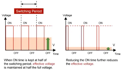
With the help of transistors, the switches are opened and closed at high frequencies, and the effective voltage obtained is made to look like that of the sine wave.
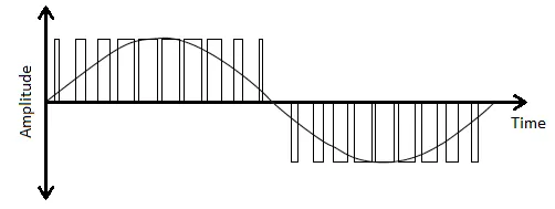
The thickness of the pulses(On-Time/Total-Time) determines the effective voltage generated.
4.
AC motors are often used in equipment that runs at a constant speed regardless of the load, such as fans, pumps, and conveyors. But when speed control is required, an AC motor is paired with a Variable Frequency Drive(VFD), which regulates the motor’s speed by using one of two control methods — scalar control or vector control — to vary the frequency of the supplied voltage.
Rotational speed N of an induction motor can be shown by the expression
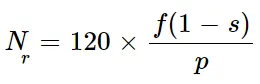
When the voltage applied to the motor is increased and decreased, the slip s changes, then the rotational speed N will change.
N: Rotational speed [r/min]
F: Frequency 〔Hz〕
P: Number of poles of a motor
S: Slip
Since the Number of poles is fixed, the speed of the motor can be controlled by varying the frequency.
A Variable Frequency Drive is a type of motor controller that drives an electric motor by varying the frequency and voltage supplied to the electric motor. The speed of the motor can be controlled by varying the parameters of the input signal.
The earliest VFDs used linear amplifiers to control all aspects of the VFD. Jumpers and dip switches were used to provide ramp-up (acceleration) and ramp-down (deceleration) features by switching larger or smaller resistors into circuits with capacitors to create different slopes.
Newer VFDs provide methods of braking, power boost during ramp-up, and a variety of controls during ramp-down. The biggest savings that the VFD provides is that it can ensure that the motor doesn't pull excessive current when it starts, so the overall demand factor for the entire factory can be controlled to keep the utility bill as low as possible.
Today the VFD is the most common type of output or load for a control system. VFDs are also available in smaller sizes that are cost-efficient and take up less space.
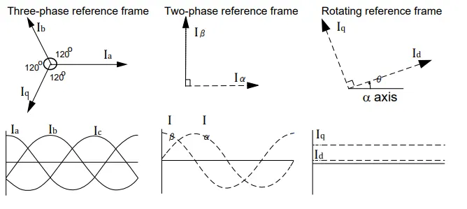
Vector control method: The vector control method of controlling the AC motor is based on the reference frame transformation theory.
Vector control is characterized by involving the phase and magnitude of the applied voltage.
Vector control is preferred for its following characteristics:
- Precise control of motor
- Excellent dynamic response
- High-performance drives
- Low power dissipation
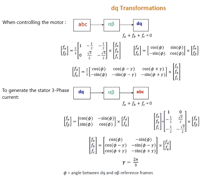
Clarks transformation: Clarks transformation converts balanced three-phase quantities into balanced two-phase quadrature quantities.
Parks transformation: Parks transformation converts vectors in balanced two-phase orthogonal stationary system into orthogonal rotating
reference frame.