Week 6.1 - Setting up a model (Electronic enclosure)
AIM
The objective of the project is to setup the physics for the model and the solve the model.
TASK
- Setup the physics for the Electronic enclosure.
- Solve the Electronic enclosure and display the results.
Model
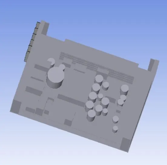
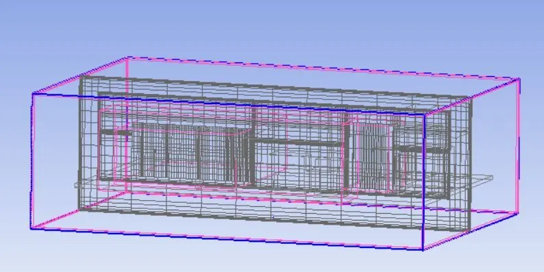
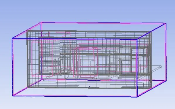
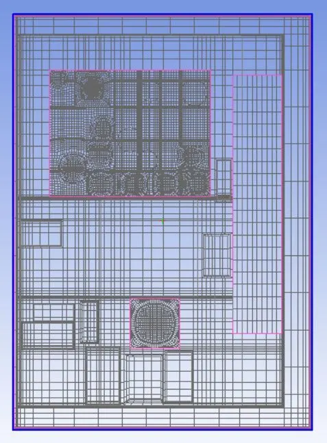
The total of 11 assembly are created for the model
The enclosure are divided into separate assembly for the model depending on the meshing technique and slack is set to zero since the enclosure are attached the slack causes overlap of assemble.
Assemble 1
i) Mesh type
Max element size X - 0.4mm.
Max element size Y - 3.5mm.
Max element size Z - 2.5mm.
Min Gap X - 0.08 mm.
Min Gap Y - 1 mm.
Min Gap Z - 0.5 mm.
Assemble 2
i) Mesh type
Max element size X - 0.4mm.
Max element size Y - 8.5mm.
Max element size Z - 2.5mm.
Min Gap X - 0.08 mm.
Min Gap Y - 4 mm.
Min Gap Z - 0.5 mm.
Assemble 3
i) Mesh type
Max element size X - 6mm.
Max element size Y - 8.5mm.
Max element size Z - 0.4mm.
Min Gap X - 3 mm.
Min Gap Y - 4 mm.
Min Gap Z - 0.08 mm.
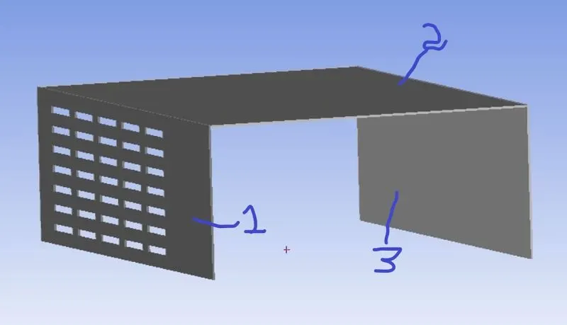
Assembe 4
i) Mesh type
Max element size X - 3.5 mm.
Max element size Y - 0.4 mm.
Max element size Z - 2.5 mm.
Min Gap X - 1 mm.
Min Gap Y - 0.08 mm.
Min Gap Z - 0.5 mm.
Assemble 5
i) Mesh type
Max element size X - 6mm.
Max element size Y - 8.5 mm.
Max element size Z - 0.4 mm.
Min Gap X - 3 mm.
Min Gap Y - 4 mm.
Min Gap Z - 0.08 mm.
Assemble 6
i) Mesh type
Max element size X - 3.5mm.
Max element size Y - 0.4 mm.
Max element size Z - 2.5 mm.
Min Gap X - 1 mm.
Min Gap Y - 0.08 mm.
Min Gap Z - 0.5 mm.
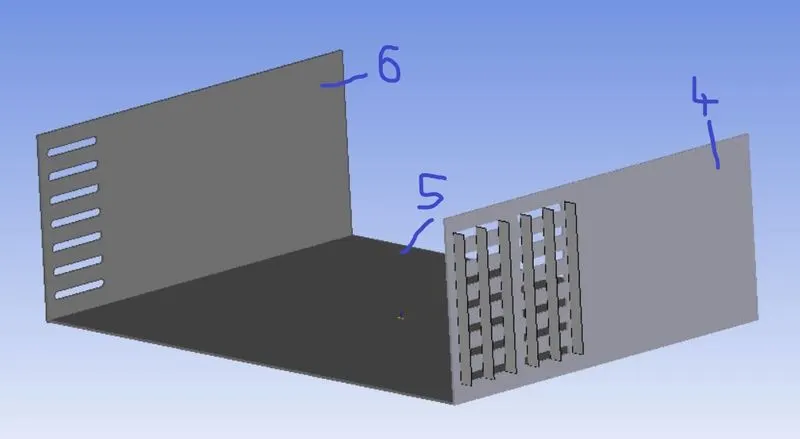
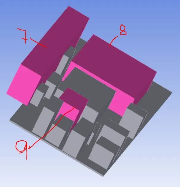
The PCB is divided into 4 assembly to create a non confromal mesh for the model
Assemble 7
i) Mesh type
Max element size X - 4 mm.
Max element size Y - 10 mm.
Max element size Z - 3 mm.
Min Gap X - 2 mm.
Min Gap Y - 5 mm.
Min Gap Z - 0.5 mm.
Assemble 8
i) Slack setting
Min X - 1 mm.
Max X - 1 mm.
Min Y - 1 mm.
Max Y - 1 mm.
Min Z - 0.
Max Z - 1 mm.
ii) Mesh type
Max element size X - 1 mm.
Max element size Y - 1 mm.
Max element size Z - 5 mm.
Min Gap X - 0.05 mm.
Min Gap Y - 0.05 mm.
Min Gap Z - 1 mm.
Assemble 9
i) Slack setting
Min X - 1 mm.
Max X - 1 mm.
Min Y - 1 mm.
Max Y - 1 mm.
Min Z - 0.
Max Z - 1 mm.
ii) Mesh type
Max element size X - 1 mm.
Max element size Y - 1 mm.
Max element size Z - 5 mm.
Min Gap X - 0.05 mm.
Min Gap Y - 0.05 mm.
Min Gap Z - 1 mm.
Assemble 10
i) Mesh type
Max element size X - 4.5 mm.
Max element size Y - 7.5 mm.
Max element size Z - 2 mm.
Min Gap X - 0.5 mm.
Min Gap Y - 1.25 mm.
Min Gap Z - 0.08 mm.
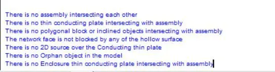
Macros --> Productivity --> Validation --> Automatic case check tool - This option check for the model on various criteria.
Mesh Control
X Cut plane
Y Cut plane
Z Cut plane
Mesh Verification
Face alignment
- It is the measure of mesh quality defined by face alignment index = C0C1.f
- C0 & C1 are the centroids of two adjacent elements are normal vector to the face between the two elements.
- Range of face alignment 0 (bad) to 1 (good) & value greater than 0.1 (preferred) & value greater than 0.15 provide better results.
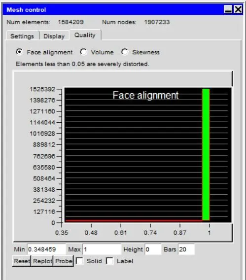
The min value of the model is 0.348 and value greater than 0.15 provide accurate results
Volume
- Preferable volume of mesh to be greater than 1e-13 for single precision solver & greater than 1e-15 for double precision.
- Max / Min cell volume should be less than 10^7 for single precision & must be less than 10^12 for double precicion since very small volume create divergence of the solution.
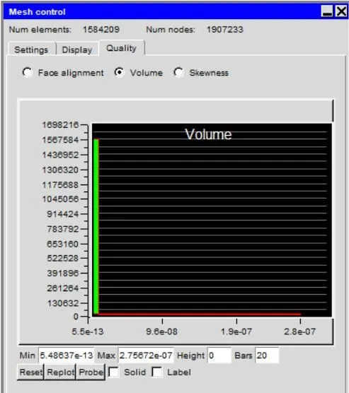
The volume of the mesh greater than 10^-13 & Max / Min cell ratio is around 2 * 10^6 which is in required range & the single precision is used for this model.
Skewness
It determines how close to the ideal & based on the equilateral volume. The value greater than 0.5 provide good cell quality.
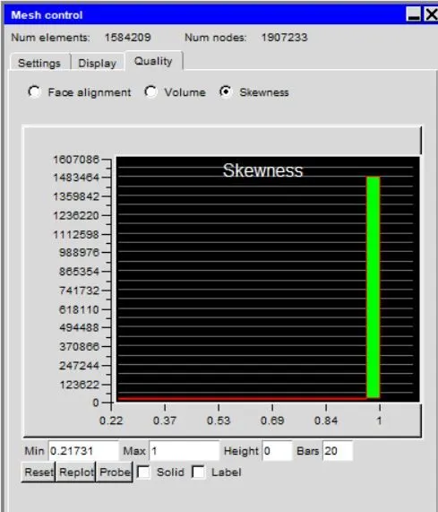
The min value of the skewness is 0.217 and the PCB board has many components which are too close which causes the distortion of the elements so the skewness value is low.
Solver
The three dimensional steady state Navier stokes equations for the model are solved within the computational domain.
General Setup
- Variables solved - flow and temperature.
- Radiation - Off.
- Flow regime - Turbulent - The zero equation are solved for the turbulent model.
The natural convection are not consider for this model & also gravity vector are not consider.
The defaults value of the parameters are set to default.
Transient Setup
- Time variation - Steady
Solution Initialization
X velocity - 0.
Y velocity - 0.5 m/s.
Z velocity -0.
Temperature - ambient.
Basic settings
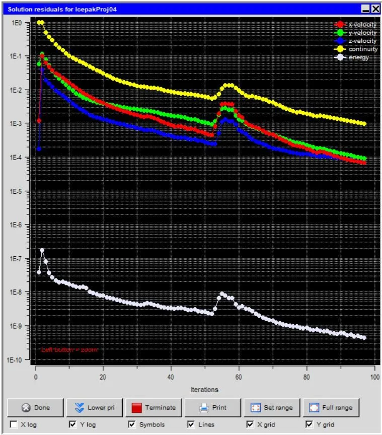
No of iterations - 100.
Convergence criteria
Flow - 0.001.
Energy - 1e-7.
Joule heating - 1e-7.
Parallel Settings
Configuration - parallel.
Parallel options - 2 processors.
Advance Solver Setup
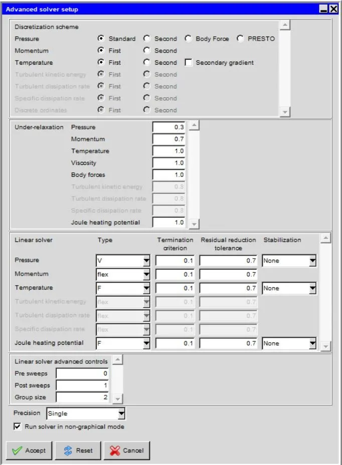
Results
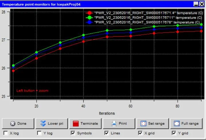
Monitor points
Residual plot
Contour plot
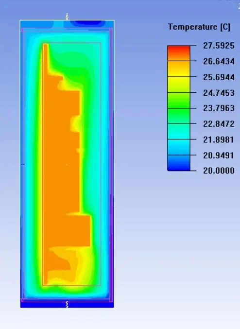
Temperature plot
ZY Plane
ZX Plane
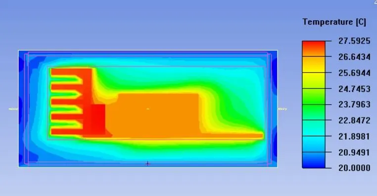
XY Plane
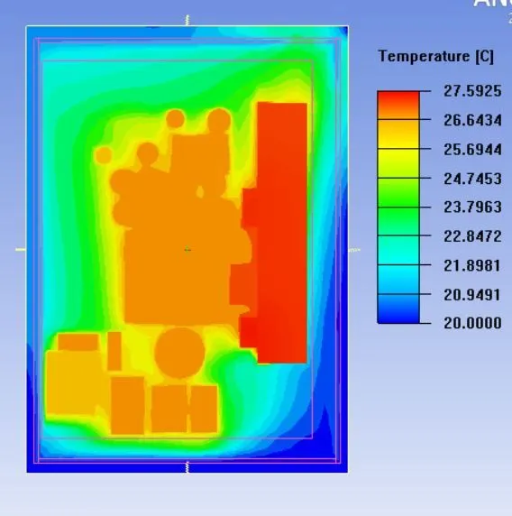
The heat are the two mosfet attached to the fins so the maximum temperature is around the fins which is 27.6 deg C and the min temp is the ambient. The heat transfer is faster in the conduction medium and the slow in convection medium.
Velocity contour
Conclusion
In this project the given model of the Electronic enclosure was meshed using ANSYS Icepak using the non-conformal meshing, per-object meshing parameters and multi-level meshing. The three dimensional steady-state governing equations for the model were solved for flow and temperature within the computational domain in the Icepak.
- The maximum temperature within the computational domain is 27.6 deg.C.
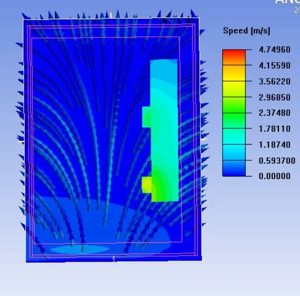
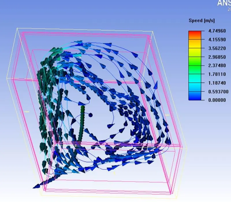
- The maximum air velocity within the computational domain is 4.75 m/s.