Week 9 - PCB Thermal Simulation
PCB Board
A printed circuit board (PCB) mechanically supports and electrically connects electronic components using conductive tracks, pads and other features etched from one or more sheet layers of copper laminated onto and/or between sheet layers of a non conductive substrate. Components are generally soldered onto the PCB to both electrically connect and mechanically fasten them to it. A basic PCB consists of a flat sheet of insulating material and a layer of copper foil, laminated to the substrate. Chemical etching divides the copper into separate conducting lines called tracks or circuit traces, pads for connections, vias to pass connections between layers of copper, and features such as solid conductive areas for electromagnetic shielding or other purposes. The tracks function as wires fixed in place, and are insulated from each other by air and the board substrate material.
AIM
The objective of the project is to create a PCB model by importing the PCB layout, library files and traces to Ansys Icepak and setup the physics & solve the thermal model.
TASK
The three cases for the following cases:
- The model is solved only for Conduction, without components.
- The model is solved for the forced convection with the actual components.
- The model is solved for the forced convection and traced heating.
Conduction only model
The trace.tzr file is unpack and the all the components are set to inactive.
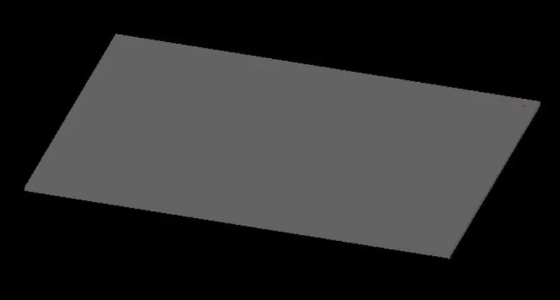
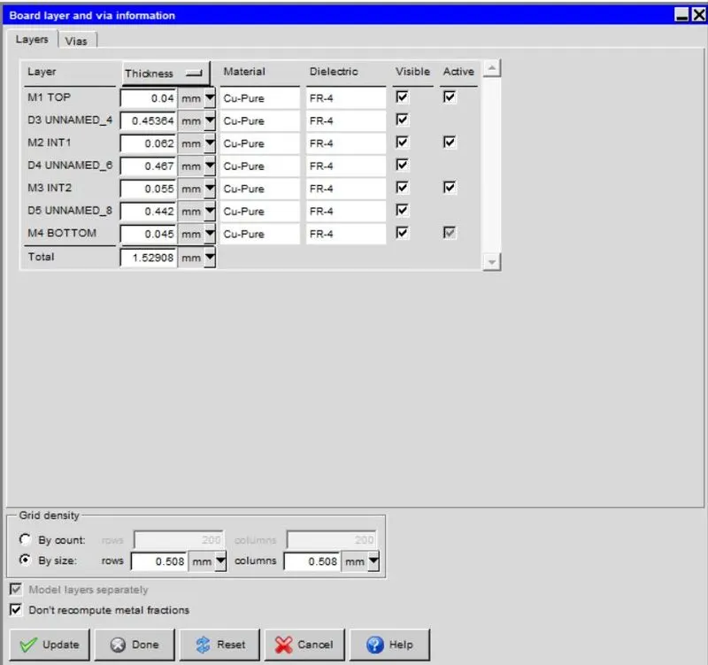
Import the ECAD file A1.anf and edit the thickness layer for the model and the grid density is set at 0.508mm * 0.508mm.
- The cabinet wall type is set to wall type as wall for the Min z & Max z and the other are set to default.
- Min z: Temperature from the External conditions drop-down list, and keep the ambient temperature (20°C).
- Max z: specify a Heat flux of 20000 W/m2 in the Thermal specification, the rest of the sides are insulated.
- The board will be simulated using a conduction-only model.
Mesh Control
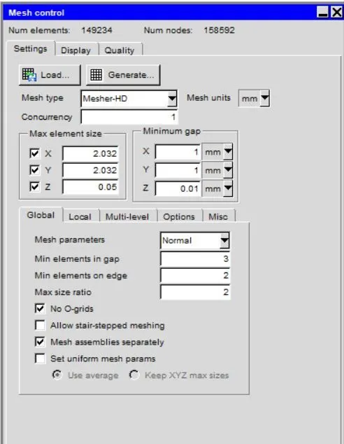
Mesh along Z plane
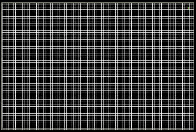
Mesh Verification
Face alignment
- It is the measure of mesh quality defined by face alignment index = C0C1.f
- C0 & C1 are the centroids of two adjacent elements are normal vector to the face between the two elements.
- Range of face alignment 0 (bad) to 1 (good) & value greater than 0.1 (preferred) & value greater than 0.15 provide better result.
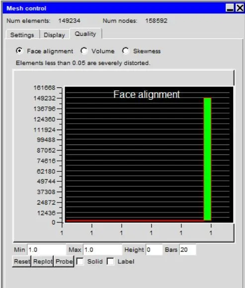
The min value of the model is 1 which is ideal for the results.
Volume
- Preferable volume of mesh to be greater than 1e-13 for single precision solver & greater than 1e-15 for double precision.
- Max / Min cell volume should be less than 10^7 for single precision & must be less than 10^12 for double precicion since very small volume create divergence of the solution.
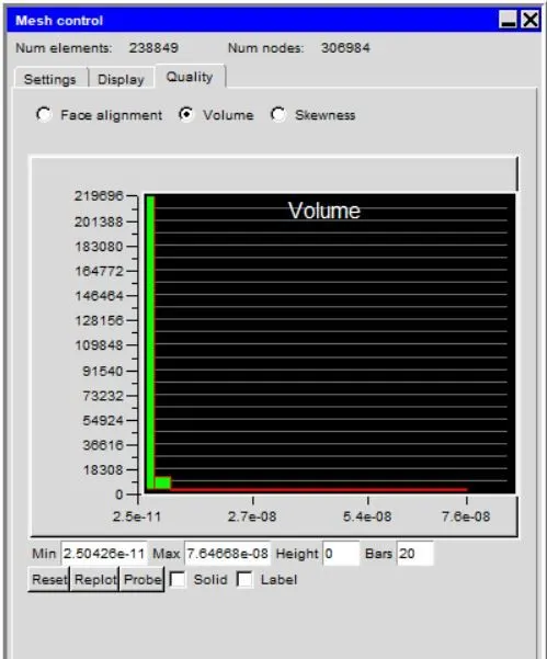
The volume of the mesh greater than 10^-13 & Max / Min cell ratio is around 3e3 which is in required range & the single precision can be used for this model.
Skewness
It determines how close to the ideal & based on the equilateral volume. The value greater than 0.5 provide good cell quality.
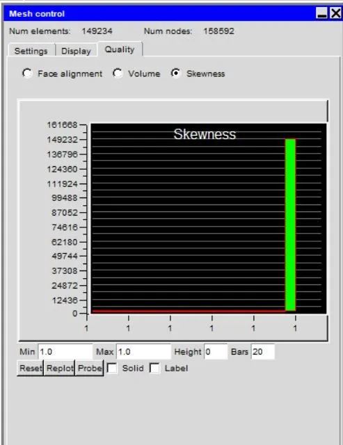
The min value of the skewness is 1 so only ideal element are formed.
Solver
The three dimensional steady state Navier stokes equations for the model are solved within the computational domain.
General Setup
- Variables solved - temperature.
- Radiation - Off.
- Flow regime - Turbulent - The zero equation are solved for the turbulent model.
The defaults value of the parameters are set to default.
Transient Setup
- Time variation - Steady
Solution Initialization
X velocity - -1.
Y velocity - 0.
Z velocity -0.
Temperature - ambient.
Basic settings
No of iterations - 500.
Convergence criteria
Flow - 0.001.
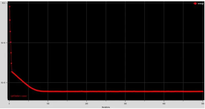
Energy - 1e-20.
Joule heating - 1e-7.
Parallel Settings
Configuration - parallel.
Parallel options - 4 processors.
Advance Solver Setup
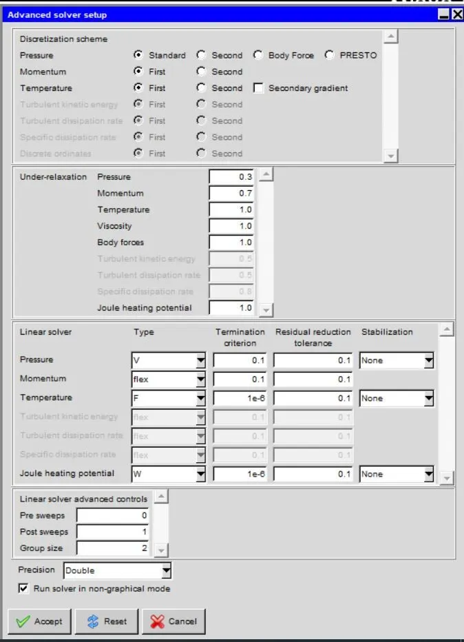
Residuals
The residuals for the energy equation are plotted against as the number of the iterations.
PCB Traces
The PCB traces of the model using the different display options.
Single colour trace
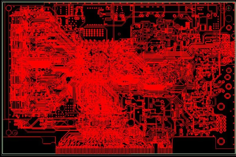
The PCB traces are displayed by a single colour.
Colour by layer traces
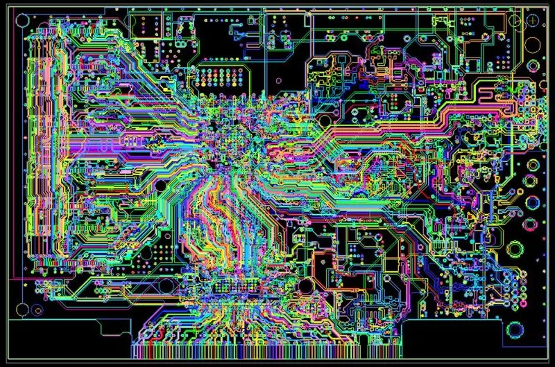
The PCB traces are displayed by a different colour.
Colour by traces
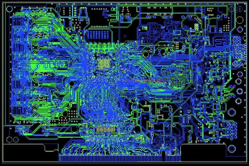
The PCB traces are displayed by different layer using different colour.
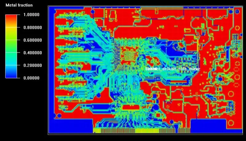
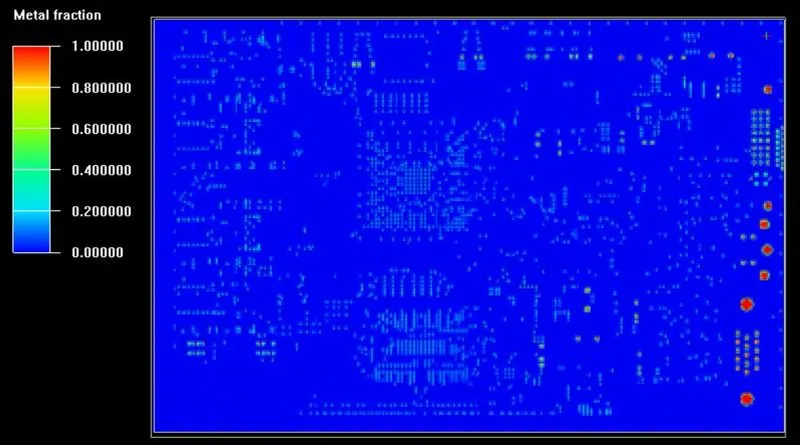
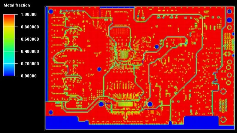
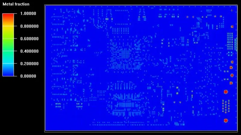
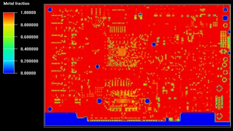
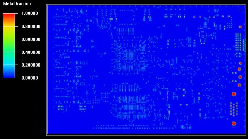
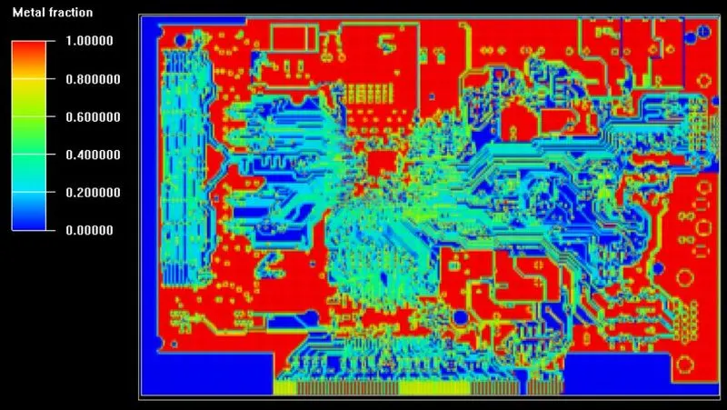
Metal traces fraction
The metal fraction contours plotted over the different layers of the PCB.
Layer 1
Layer 2
Layer 3
Layer 4
Layer 5
Layer 6
Layer 7
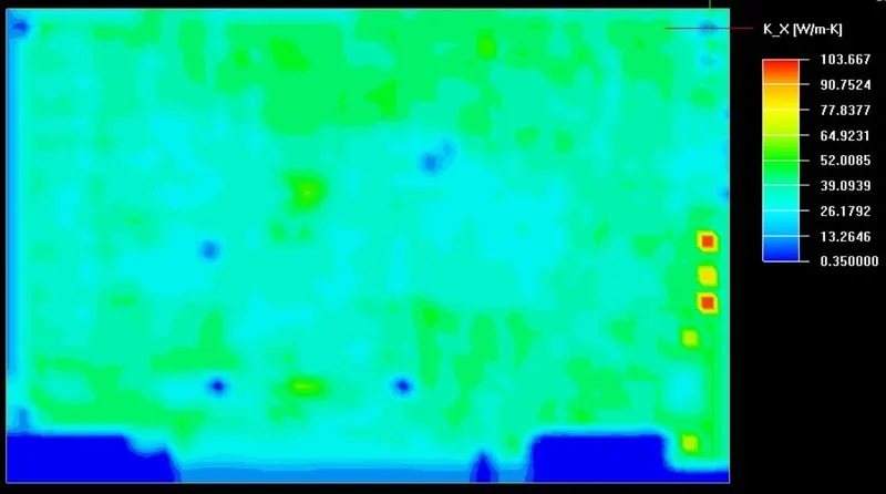
Thermal Conductivity
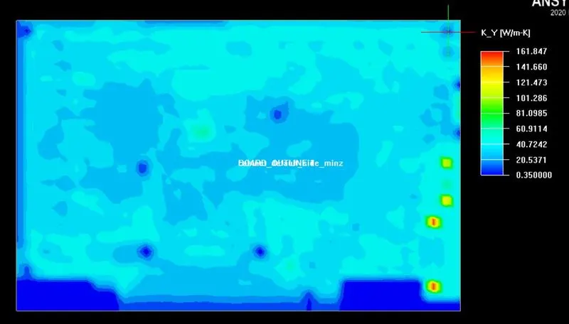
The thermal conductivity contours for the kx,ky & kz are plotted over Z plane passing through the center of the PCB.
Conductivity along X
Conductivity along Y
COnductivity along Z
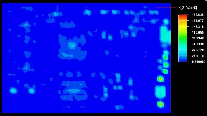
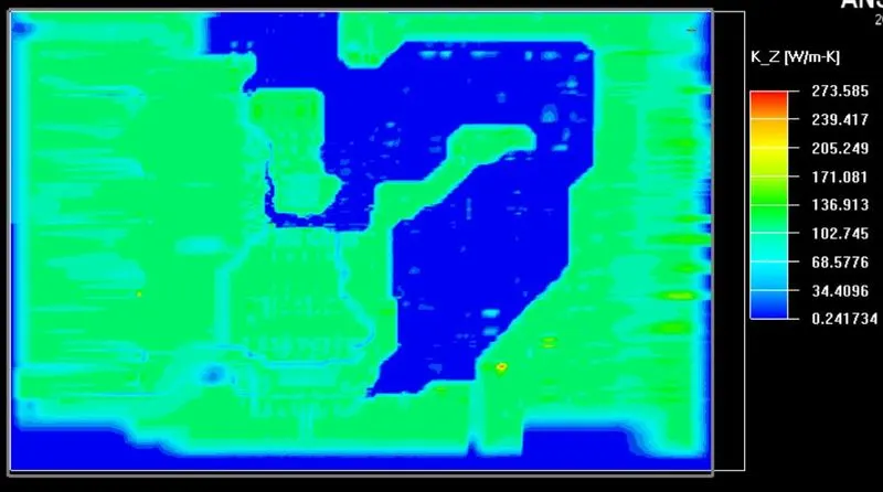
It is evident from the contours that the thermal conductivity of the PCB is anisotropic in nature.
Temperature Contour
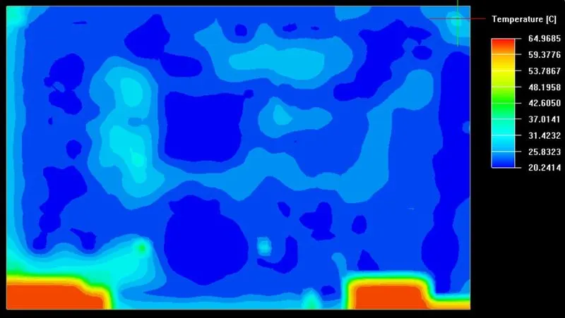
The maximum temp is 64.9685 degC for the PCB and lowest temp is 20.2414 degC.
Velocity Contour
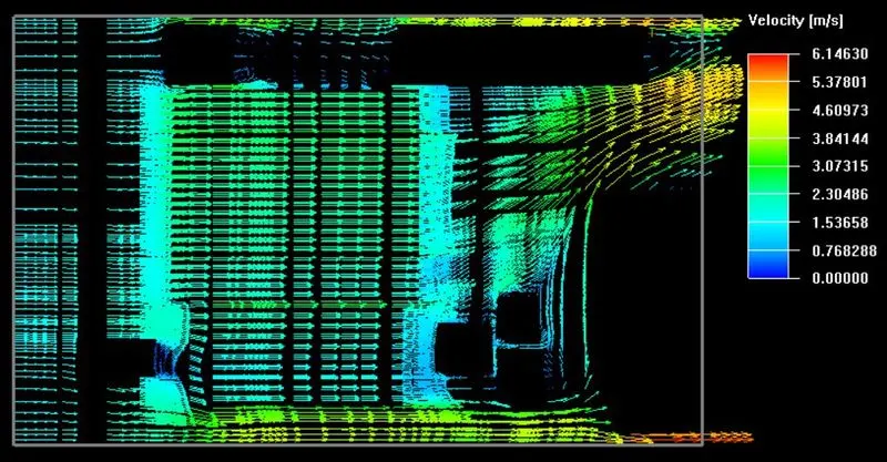
The max velocity is 6.1463 m/s and is at the max x side. The air flow around the PCB components.
Forced Convection model
- The active all the components which were kept to inactive in the conduction model.
- The two wall object created for the ''conduction only" model and drag them into the inactive folder.
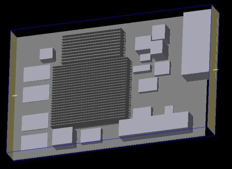
- Click on the cabinet and autoscale it form the edit window.
- The cabinet wall type is set to wall type as opening for the Min x & Max x and the other are set to default.
- Max x: assign an X velocity of -1.5 m/s for Max x side of the cabinet
- The board will be simulated using a forced convection model.
Mesh control
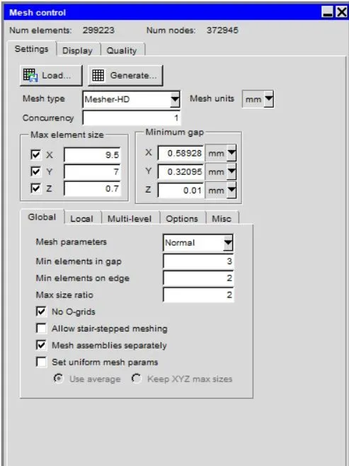
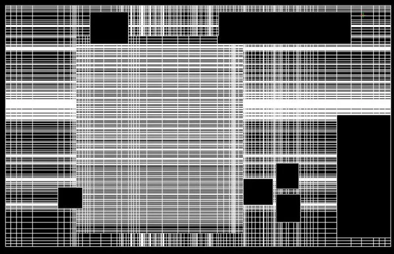
Mesh along X plane

Mesh along Y plane

Mesh along Z plane
Mesh Verification
Face alignment
- It is the measure of mesh quality defined by face alignment index = C0C1.f
- C0 & C1 are the centroids of two adjacent elements are normal vector to the face between the two elements.
- Range of face alignment 0 (bad) to 1 (good) & value greater than 0.1 (preferred) & value greater than 0.15 provide better result.
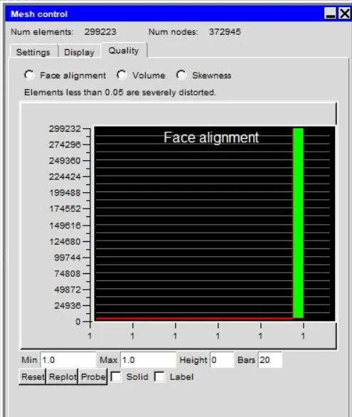
The min value of the model is 1 which is ideal for the results.
Volume
- Preferable volume of mesh to be greater than 1e-13 for single precision solver & greater than 1e-15 for double precision.
- Max / Min cell volume should be less than 10^7 for single precision & must be less than 10^12 for double precicion since very small volume create divergence of the solution.
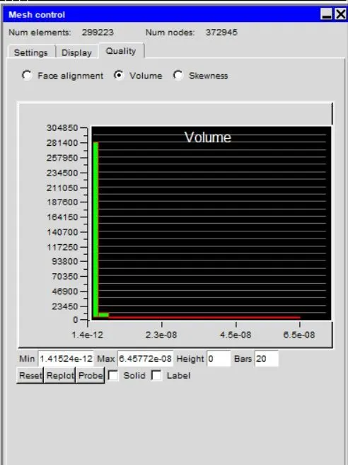
The volume of the mesh greater than 10^-13 & Max / Min cell ratio is around 4.5e4 which is in required range & the double precision can be used for this model.
Skewness
It determines how close to the ideal & based on the equilateral volume. The value greater than 0.5 provide good cell quality.
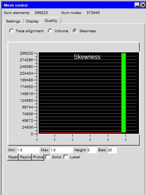
The min value of the skewness is 1 so only ideal element are formed.
Solver
The three dimensional steady state Navier stokes equations for the model are solved within the computational domain.
General Setup
- Variables solved - flow & temperature.
- Radiation - Off.
- Flow regime - Turbulent - The zero equation are solved for the turbulent model.
The defaults value of the parameters are set to default.
Transient Setup
- Time variation - Steady
Solution Initialization
X velocity - -1.
Y velocity - 0.
Z velocity -0.
Temperature - ambient.
Basic settings
No of iterations - 500.
Convergence criteria
Flow - 0.001.
Energy - 1e-20.
Joule heating - 1e-7.
Parallel Settings
Configuration - parallel.
Parallel options - 4 processors.
Advance Solver Setup
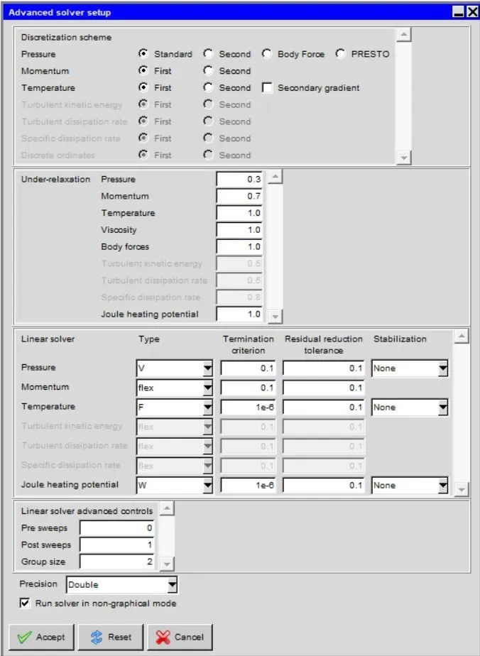
PCB Traces
The PCB traces of the model are same as that of the conduction model since the same model is used for thr both simulation
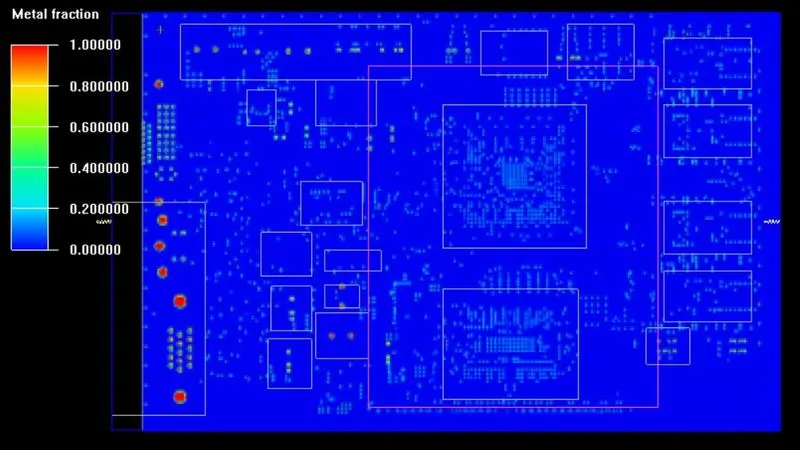
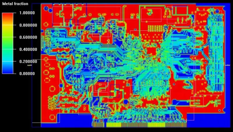
Metal traces fraction
The metal fraction contours plotted over the different layers of the PCB.
Layer 1
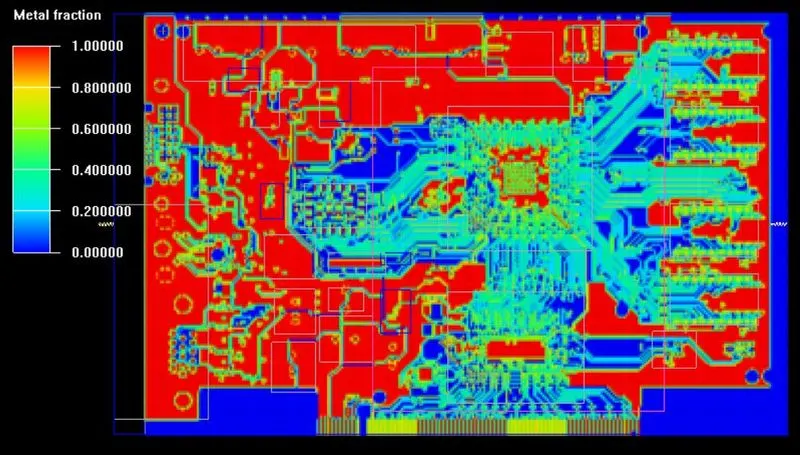
Layer 2
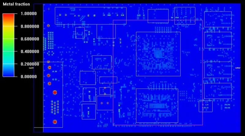
Layer 3
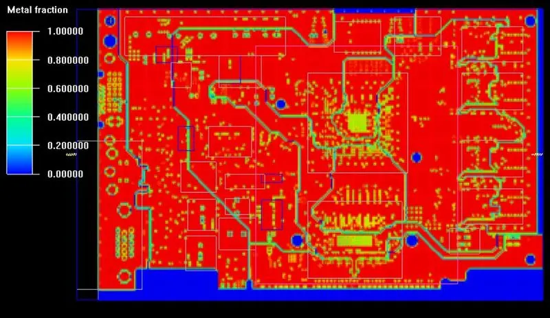
Layer 4
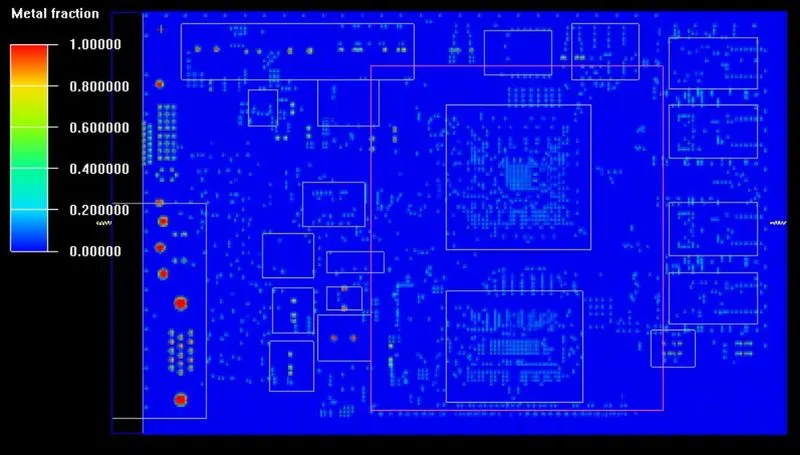
Layer 5
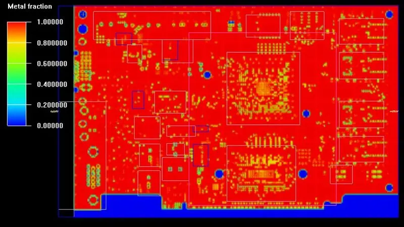
Layer 6
Layer 7
Thermal Conductivity
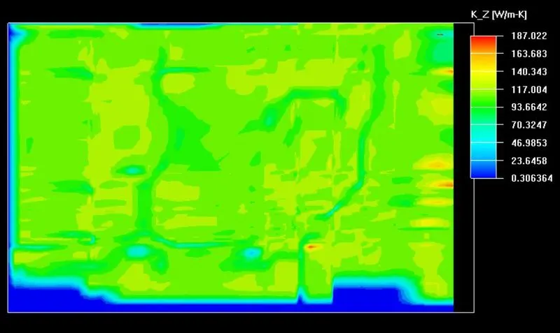
The thermal conductivity contours for the kx,ky & kz are plotted over Z plane passing through the center of the PCB.
Conductivity along Z
Temperature Contour
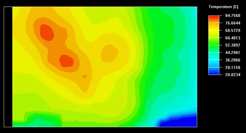
The maximum temp is 84.756 degC for the PCB and lowest temp is 20.0234 degC.
Velocity Contour
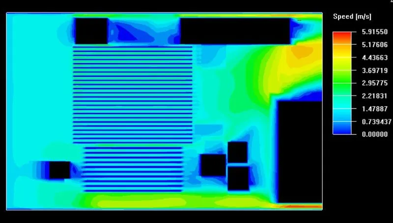
The max velocity is 5.9155 m/s and is at the max x side. The air flow around the PCB components.
Forced Convection with trace heating
The PCB traces have electrical resistance which gets heat up as current flows through them, so modeling this phenomenon will provide us with an accurate prediction of the temperature distribution in the PCB. The solid trace for the PCB is created.
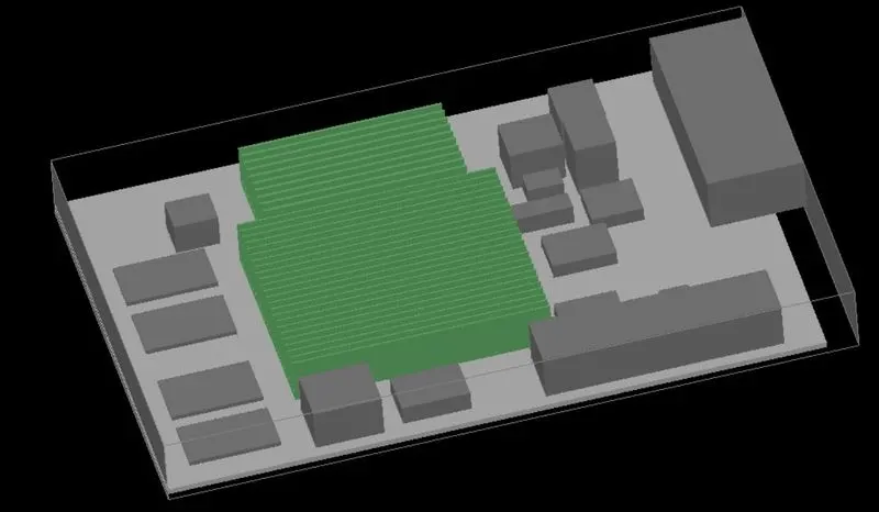
- Edit the Board outline of the previous model to open the model trace heating. panel --> select INT1_3 layer, and under display filter group box provide a Min Area of 4124 mm2.
- Before you create a solid trace of trace A3V3_2261 set the Max angle filter to 135 and the Min length filter to 1.0 m to ignore the fine details in the trace geometry and reduce the mesh count and click on create a solid trace.
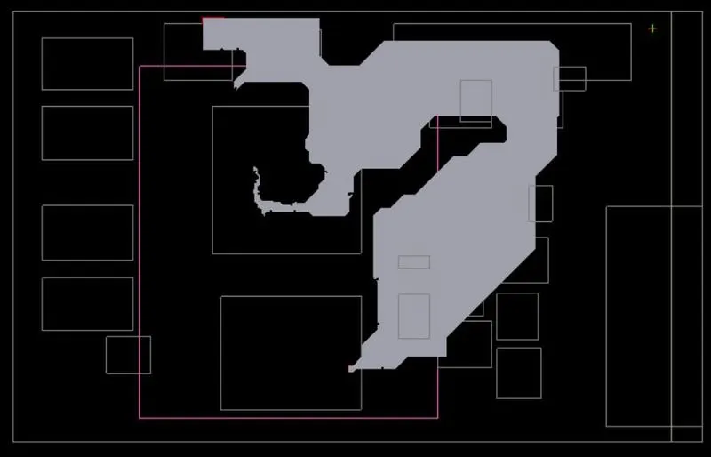
- The two voltage/current type sources are created on the solid trace.
Source 1
i) Geometry
Shape - Rectangular.
Plane - X-Y.
Specified By - Start/length.
Start Xs - 108.7 mm.
Start Ys - 1.35 mm.
Start Zs - 1.071 mm.
Length Xl - 114.05 mm.
Length Yl - 2.8 mm.
Source 2
i) Geometry
Shape - Rectangular.
Plane - X-Y.
Specified By - Start/length.
Start Xs - 71.5 mm.
Start Ys - -86.23 mm.
Start Zs - 1.071 mm.
Length Xl - 76.8 mm.
Length Yl - -85.34 mm.
The current value is set to 25 A for the heat source 1.
Mesh Control
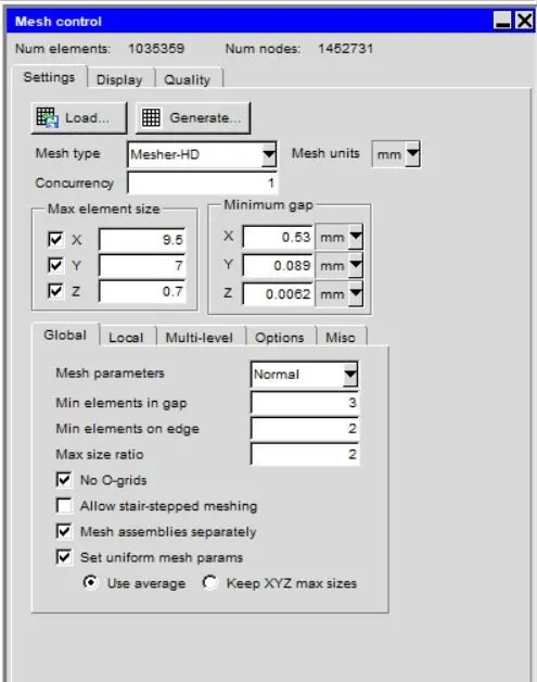
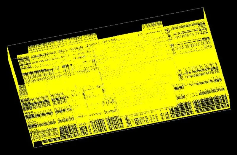
Surface mesh
Mesh Verification
Face alignment
- It is the measure of mesh quality defined by face alignment index = C0C1.f
- C0 & C1 are the centroids of two adjacent elements are normal vector to the face between the two elements.
- Range of face alignment 0 (bad) to 1 (good) & value greater than 0.1 (preferred) & value greater than 0.15 provide better result.
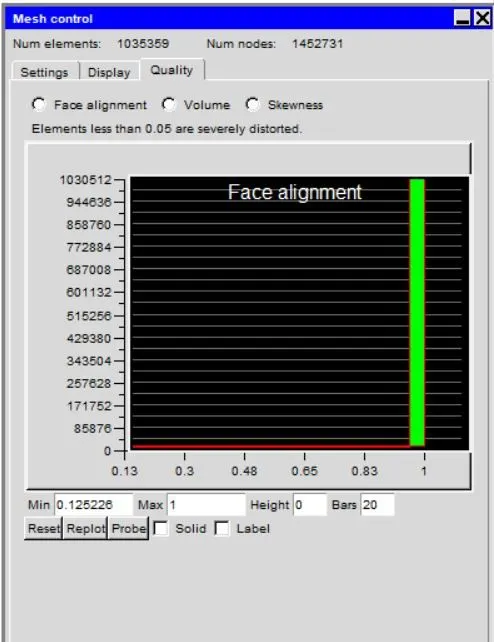
The min value of the model is 0.125 which is greater than 0.1 which is preferred for the simulation.
Volume
- Preferable volume of mesh to be greater than 1e-13 for single precision solver & greater than 1e-15 for double precision.
- Max / Min cell volume should be less than 10^7 for single precision & must be less than 10^12 for double precicion since very small volume create divergence of the solution.
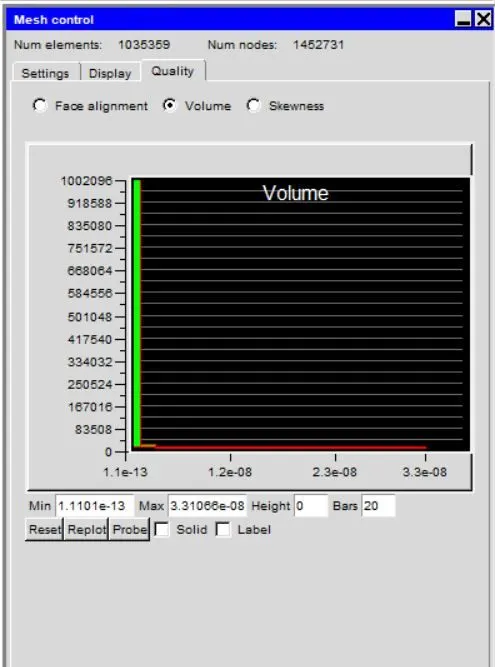
The volume of the mesh greater than 10^-13 & Max / Min cell ratio is around 3e5 which is in required range & the double precision can be used for this model.
Skewness
It determines how close to the ideal & based on the equilateral volume. The value greater than 0.5 provide good cell quality.
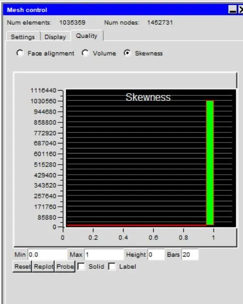
The min value of the skewness is 0 which is not preferred for the simulation to improve the skewness the mesh size & proper mesh groups must be formed.
Solver
The three dimensional steady state Navier stokes equations for the model are solved within the computational domain.
General Setup
- Variables solved - flow & temperature.
- Radiation - Off.
- Flow regime - Turbulent - The zero equation are solved for the turbulent model.
The defaults value of the parameters are set to default.
Transient Setup
- Time variation - Steady
Solution Initialization
X velocity - -1.
Y velocity - 0.
Z velocity -0.
Temperature - ambient.
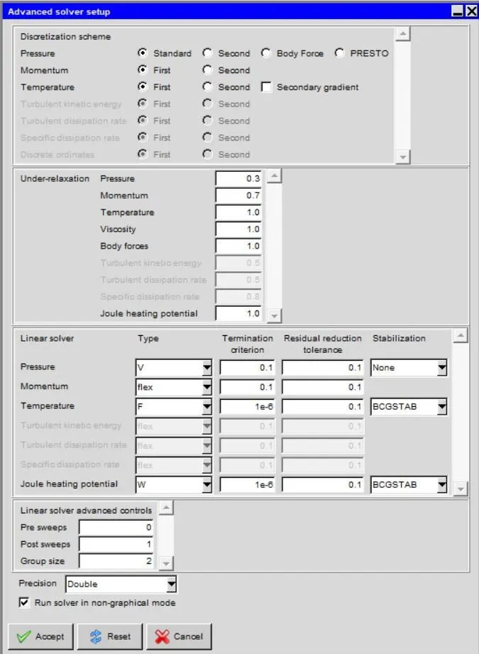
Basic settings
No of iterations - 500.
Convergence criteria
Flow - 0.0001.
Energy - 1e-8.
Joule heating - 1e-7.
Parallel Settings
Configuration - parallel.
Parallel options - 4 processors.
Advance Solver Setup
Residuals plot
The residuals for the following equations are plotted against the number of iterations:
- Continuity equation.
- X- velocity equation.
- Y- velocity equation.
- Z- velocity equation.
- Energy equation.
- uds-0.
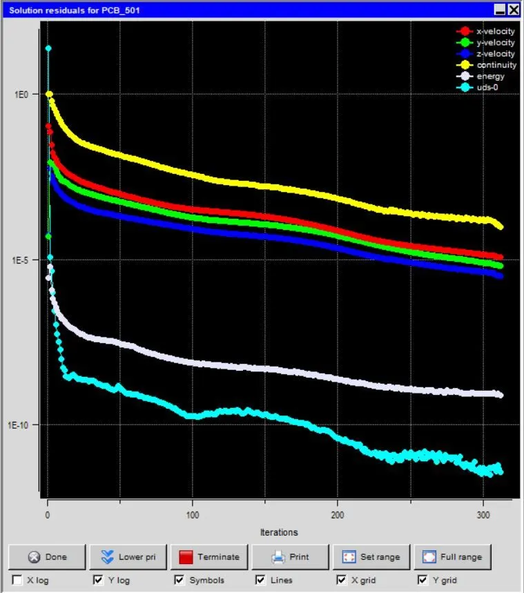
The solution has converged around 300 iterations.
PCB Traces
The PCB traces of the model using the different display options.
Single colour trace
The PCB traces are displayed by a single colour.
Colour by layer traces
The PCB traces are displayed by a different colour.
Colour by traces
The PCB traces are displayed by different layer using different colour.
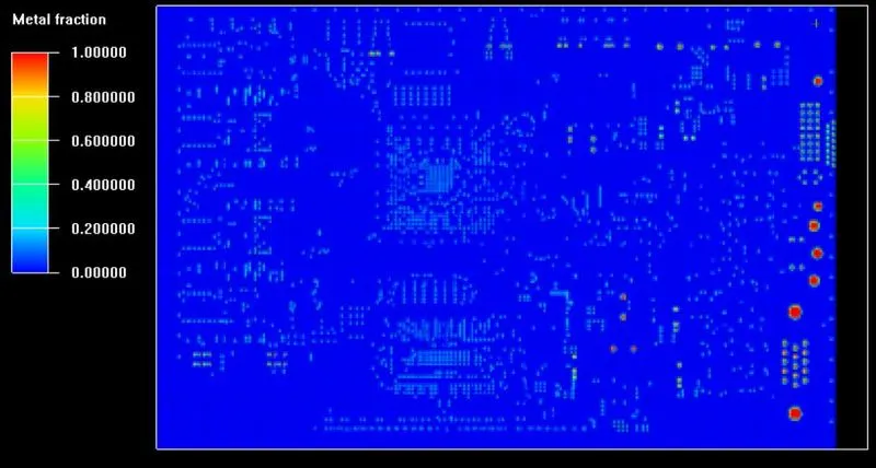
Metal traces fraction
The metal fraction contours plotted over the different layers of the PCB.
Layer 1
Layer 2
Layer 3
Layer 4
Layer 5
Layer 6
Layer 7
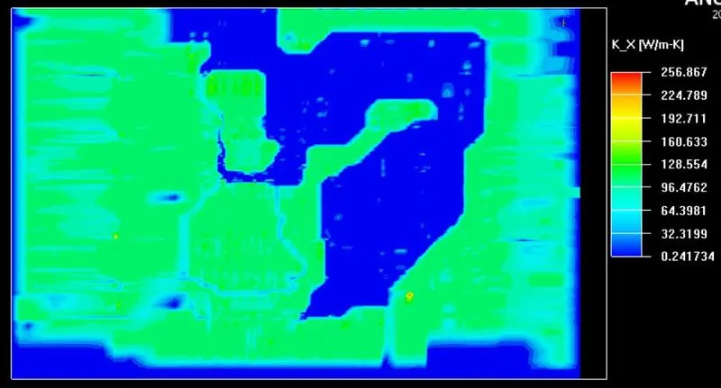
Thermal Conductivity
The thermal conductivity contours for the kx,ky & kz are plotted over Z plane passing through the center of the PCB.
Conductivity along X
Conductivity along Y
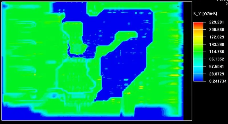
Conductivity along Z
Temperature Contour
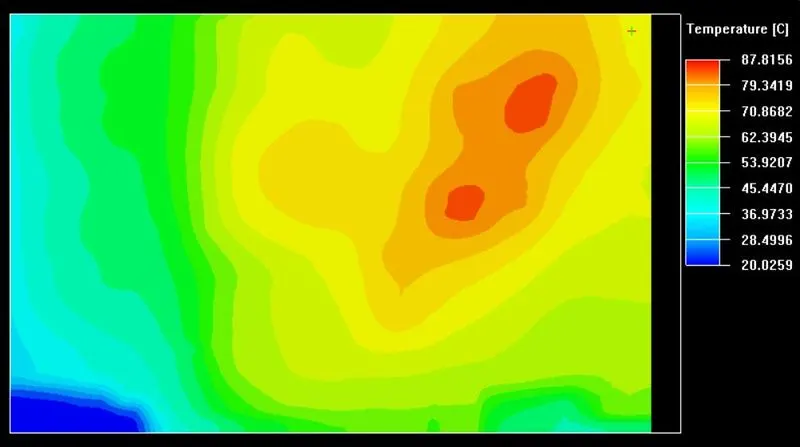
The maximum temp is 87.8156 degC for the PCB and lowest temp is 20.0259 degC.
Velocity Contour
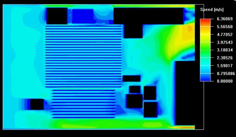
The max velocity is 6.3606 m/s and is at the max x side. The air flow around the PCB components.
Electrical potential
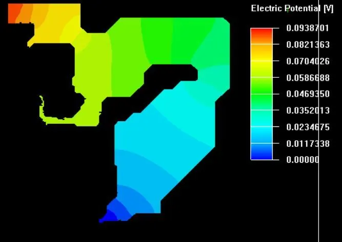
The maximum electric potential 93.87 mV on the solid trace.
Conclusion
In this project the given model of the PCB was imported into the Ansys Icepak and meshed using the non-conformal. The three dimensional steady-state governing equations for the model were solved for flow and temperature within the computational domain in the Icepak.
i) Conduction only model
All the components of the PCB were deactivated and the PCB board along with different layer are solved
- The maximum temperature within the computational domain is 64.9685 deg.C.
- The maximum air velocity within the computational domain is 6.1463 m/s.
ii) Forced convection
The components of the PCB are activated and the model is solved for the forced convection.
- The maximum temperature within the computational domain is 84.756 deg.C.
- The maximum air velocity within the computational domain is 5.9155 m/s.
iii) Forced convection with trace heating
Solid trace for the board is created and the current / voltage is applied on the solid trace and the model is solved.
- The maximum temperature within the computational domain is 87.8156 deg.C.
- The maximum air velocity within the computational domain is 6.36 m/s.