Project 1 CUK converter
Objective: Design the CUK converter in both Discuntinues Conduction Mode and Continues Conduction Mode.
Design Parameters/ Given Data:
1) Input Voltage: 30V to 60V.
2) Output Voltage: -45V.
3) Power: 1000W
Procedure:
- Calculate all required parameters like Inductance, capacitor, Load resistance.
- Design the CUK converter model in the Simulink software.
- Comper the Calculated value with simulated value.
- Comment on result and conclusion.
--------------------------------------------------------------------------------------------------------------------------------------
Continues conduction mode:
Solution:
1st we are going to Calculate all parameters for CCM.
- Duty ratio:
`V_(out)/V_(i)=-D/(1-D)`
`-45/45=-D/(1-D)`
`D=0.5`
- Load resistance:
`R=V_(out)^2/P`
`R=-45^2/1000`
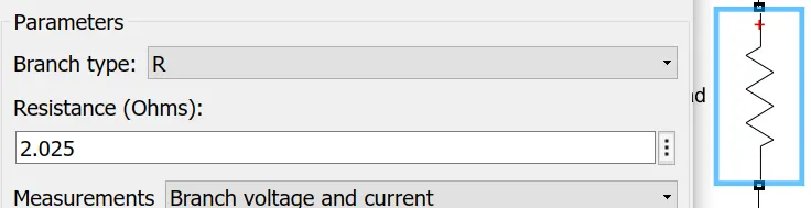
`R= 2.02 Omega`
- Input side inductance current:
`I_(l1)=P/V_i`
`I_(l1)=1000/45`
`I_(l1)=22.22A`
- Output side inductance current:
`I_(l2)=P/V_o`
`I_(l2)=1000/-45`
`I_(l1)=-22.22A`
- Input side Inductance value:
`L=V_(i)/(F_sDeltaI_l).D` Here we consider the 10% repple.
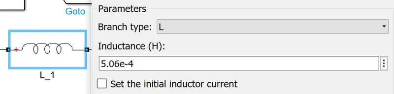
`L_1=45/(20000*2.22)*0.5`
`L_1=5.06*10^-4H`
- Output side inductance value:
`L=V_(i)/(F_sDeltaI_l).D` Here we consider the 10% repple.
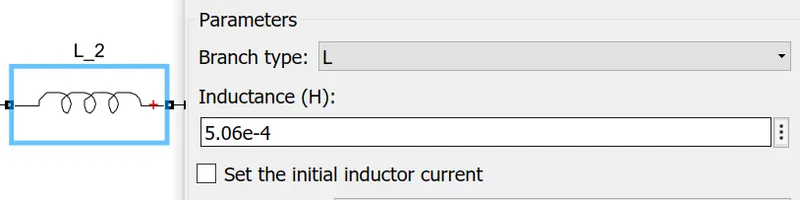
`L_2=45/(20000*-2.22)*0.5`
`L_2=5.06*10^-4`
- Input side capacitance value:
`C_1=(V_o*D)/(RF_S*DeltaV_c)` Here we consider the 1% repple.
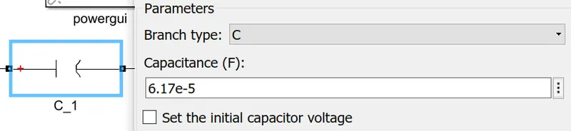
`C_1=(-45*0.5)/(2.025*20000*0.9)``
`C_1=6.1728*10^-4`
- Output side capacitance value:
`C_2=(1-D)/(8*L_2*F_s((DeltaV_o)/V_o)`
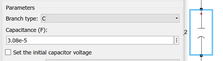
`C_2= (1-0.5)/(8*5.06*200000^2*(0.01))` Here we consider the 1% repple`
`C_1= 3.08*10^-5F`
Calculated Value:
| Duty Ratio | 0.5 |
| Load resistance | 2.025ohm |
| L_1 current | 22.22A |
| L_2 Current | -22.22A |
| L1 | 5.06*10^-4H |
| L2 | 5.06*10^-4H |
| C1 | 6.17*10^-5F |
| C2 | 3.08*10^-5F |
-------------------------------------------------------------------------------------------------------------------------
Simulink cuk converter model:
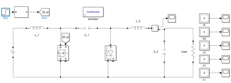
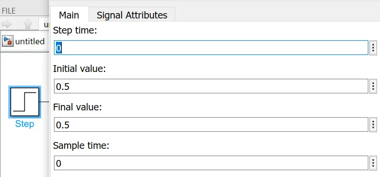
1) Duty ratio:
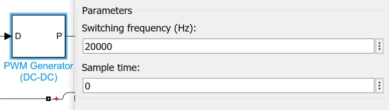
2)Switching frequency:
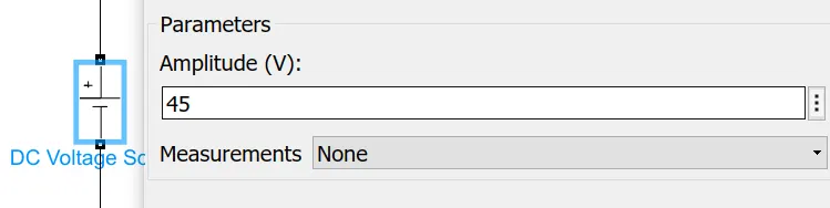
3) Input voltage:
4) Input side inductor:
5) Input side capacitor:
6) Output side inductor:
7) Output side capacitor:
8) Load resistance:
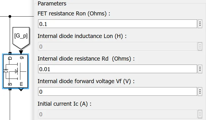
9) MOSFET:
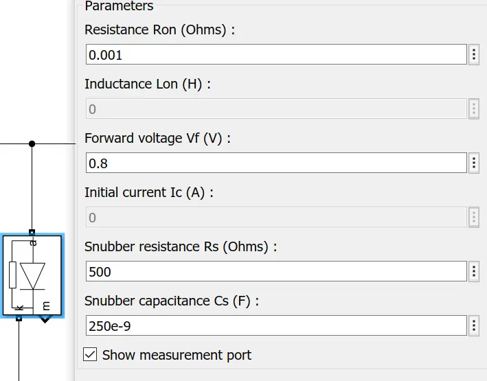
10)Diode:
---------------------------------------------------------------------------------------------------------------------------
Now run the model for simulation time 1s and get the result and compare it with the calculated values.
1) Load Voltage and current:
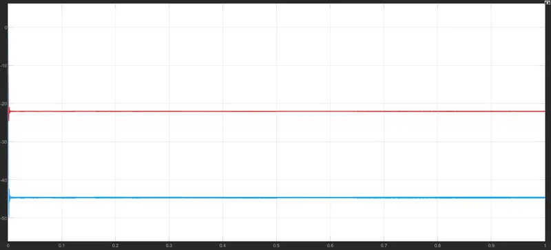
Not exactly we are getting the current and voltage as we are calculated, we are getting current -22.1A and voltage is -44.3V.
2) Output side inductor voltage and current:
voltage:
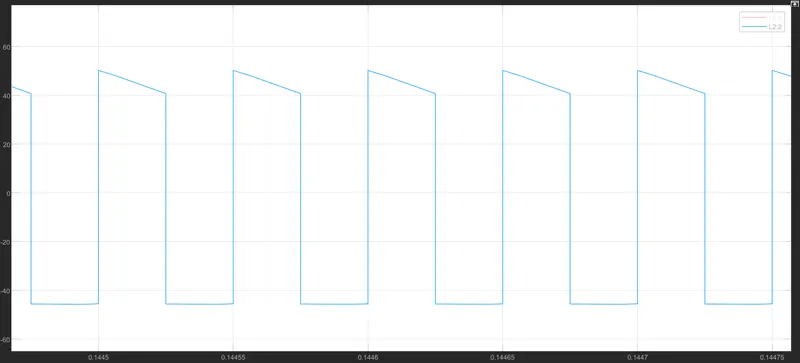
current:
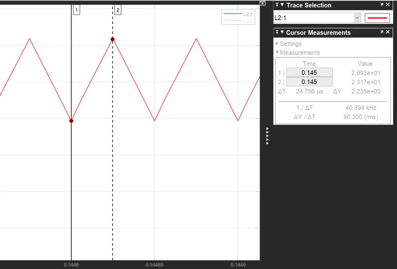
As we can see in the graph we are getting exactly the same as we are calculated value -22.22A and ripple current is also the same -2.22A
3) Output side capacitor voltage:
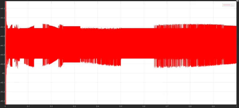
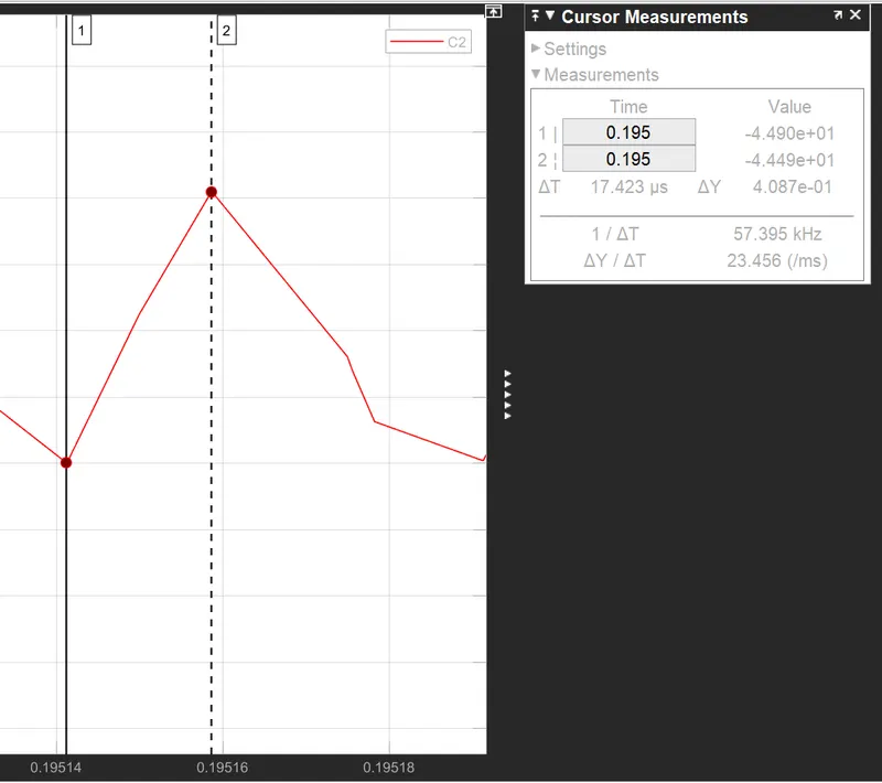
Calculated ripple voltage and graph value are near to the same calculated value are 0.45V and graph value is 0.40V.
4) Input side inductance current and voltage:
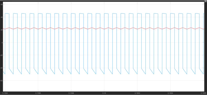
As we can see in the graph we are getting exactly the same as we are calculated value -22.22A and ripple current is also the same -2.22A
5) Input side capacitor voltage:
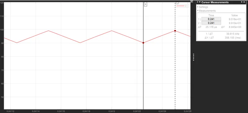
As we know, this voltage is input-output voltage so it is 90V we calculated and we are near 90V and ripple is also the same as calculated 0.9V and getting 0.8V.
----------*-----------*------------*-----------*------------*----------*-----------*------------*-----------*------------
Discontinues conduction mode:
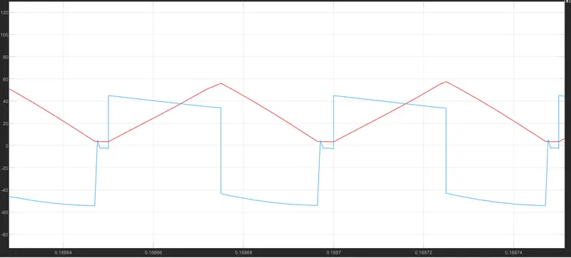
In the DCM we are using the trial and error technique, in this, we are going to do change the inductor value for which inductor current gets to cross the zero before one cycle complete.
There are some conditions that are satisfied then and then only we can say that the converter is in DCM.
- `D1< 1-D`
- `I_(Lmin) < 0`
- `Delta i_L > 2i_L`
- `L < i_(Lmin)`
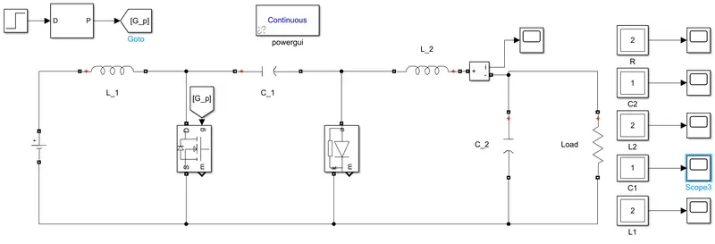
The model is the same as CCM just we are reducing the value of inductors.
Model:
Trial values:
| sr no | Input side Inductor | Output side conductor |
| 1 | `1.06e^-4` | `1.06e^-4` |
| 2 | `1.06e^-6` | `1.06e^-6` |
| 3 | `0.96e^-4` | `0.96e^-4` |
| 4 | `0.56e^-4` | `0.56e^-4` |
| 5 | `2.06e^-5` | `2.06e^-5` |
We tried more than 20 values from that we just mentioned some and the last value is that value we get the Discuntinues conduction mode which is shown in the following graphs. But all other parameters are the same as CCM just Inductor changed.
- Input sideInductor current and voltage:
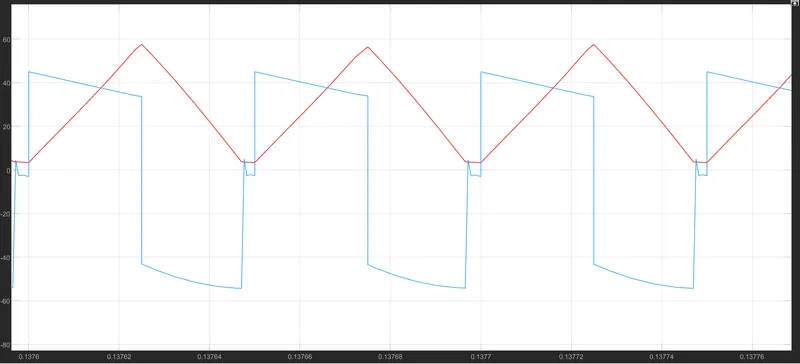
- `D1< 1-D` this condition is satisfied here.
- `I_(Lmin) < 0` current is less than zero.
- `L < i_(Lmin)` Inductor value is smaller than the Lmin.
- Output side inductor current and voltage:
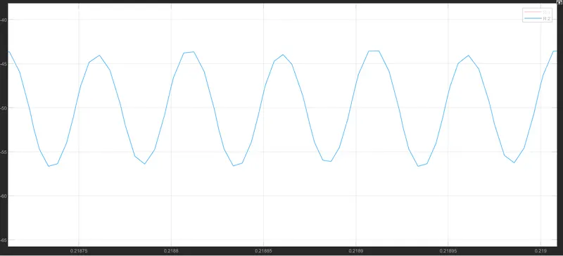
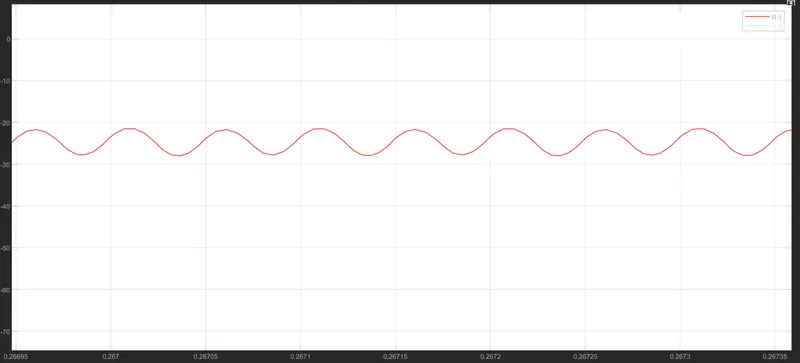
- Output voltage and current:
Voltage: Near to -45 but having more ripple.
Current: Current is the same as CCM not exactly but close to it.
--------------------------------------------------------------------------------------------------------------------------------
As we satisfied all conditions so we can say that this converter is in DCM.
From both experiment we get the following conclusion:
Efficiency:
DCM offers higher efficiency than CCM, due to the lack of reverse recovery loss on the diode and a softer turn-on of the MOSFET. However, if the duty cycle is too small, then the current that charges the primary inductor will be very high, which lowers the converter’s overall efficiency. Thus, a reasonable duty cycle must be chosen for DCM to take advantage of this benefit.
Regulation:
Regarding regulation and stability of the system, a flyback in DCM is easier to compensate than a flyback in CCM. This is because the problematic right-hand plane zero (RHPZ) appears and introduces instability at lower frequencies when the converter operates in CCM. DCM pushes the RHPZ to higher frequencies, making the loop easier to compensate, and therefore offering a faster transient response than CCM.
Furthermore, when working with duty cycles above 0.5, subharmonic oscillation may occur in CCM flyback converters, which means slope compensation is required.
Because DCM charges and discharges the inductor completely, the primary current ripple is logically much greater than in CCM. This current ripple generates a variating signal, which is then propagated due to the antenna-like behavior of the different components in the primary current loop, generating significant levels of electromagnetic interference (EMI).
On the other hand, DCM flyback converters also implement zero-current switching (ZCS), which makes it more energy-efficient, as it reduces the rectifier diode’s reverse recovery. This soft-switching affects efficiency and has a strong effect on EMI because the fast-recovery diodes that must be used in order to reduce energy loss also generate very sharp voltage spikes in the secondary side, which cause ringing and can be a source for high-frequency differential-mode noise. To solve this, a snubbing circuit must be implemented to reduce these peaks and ensure compliance with electromagnetic compatibility (EMC) standards and regulations.
| Variable | DCM | CCM |
| Efficiency | Higher | Lower |
| MOSFET VDS_MAX | Same | |
| MOSFET ID_MAX (IP_MAX) | Higher | Lower |
| Rectifier Diode Reverse Voltage Peak (VD_PK) | Same | |
| Rectifier Diode Current Peak ID1_PK (IS_PK) | Higher | Lower |
| RMS Current and Ripple | Higher | Smaller |
| Transformer Size | Smaller | Larger |
| EMI | Higher requires larger capacitors and filters | Lower, smaller capacitors and filters |
| Cross-Regulation | Higher variation | Lower variation |
| Transient Response | Faster | Slower |
| Stability |
|
|