Design and simulation of a voltage-controlled Buck converter feedback circuit
Aim: To design and simulate a buck converter with a voltage-control analog feedback circuit and obtain the required waveforms.
Procedure:
Given that:
Input Voltage (`V_i`) = 50 V
Duty ratio (D) = 0.4 or 40%
Switching Inductor (L) = 3 mH
Output Capacitor (C) = `100 muF`
Switching Frequency (`F_s`) = 20 kHz
Load Resistance (R) = `20 Omega`
Calculations:
The Voltage ratio of a buck converter is
`V_o/V_i = D`
`therefore V_o = D*V_i`
`therefore V_o = 0.4*50 = 20 V`
Therefore, the output voltage of the designed buck converter should be 20 V.
Now, for designing a feedback circuit we have to assume some parameters, like
Equivalent Series Resistance of the Capacitor (`R_(ESR)`) = `8 mOmega`
Ramp Voltage (`V_(ramp)`) = 2.5 V
Reference Voltage (`V_(ref)`) = 8 V
Oscillatory Voltage (`V_(osc)`) = 20 V
Now, calculating the poles and zeros of the converter
Frequency of the double poles (`F_(LC)`) = `1/(2pisqrt(LC))`
`therefore F_(LC) = 1/(2pisqrt(3*10^-3*100*10^-6)) = 290.57 Hz`
The frequency at zero (`F_(ESR)`) = `1/(2pi*R_(ESR)*C)`
`therefore F_(ESR) = 1/(2pi*8*10^-3*100*10^-6) = 199 kHz`
Assuming the crossover frequency to be 1/5 of the switching frequency
`therefore F_o = F_s/5`
`therefore F_o = 20000/5 = 4000 = 4 kHz`
Since, `F_(LC) < F_o < F_s/2 < F_(ESR)`, type III-B compensator is suitable for this application.
The compensator poles and zeros are chosen `70^o` phase lead at the crossover frequency.
Now, calculating the poles and zeros of the compensator
`F_(Z2) = F_osqrt((1-sintheta)/(1+sintheta))`
`therefore F_(Z2) = 4000sqrt((1-sin70^o)/(1+sin70^o)) = 705.3 Hz`
`F_(P2) = F_osqrt((1+sintheta)/(1-sintheta))`
`therefore F_(P2) = 4000sqrt((1+sin70^o)/(1-sin70^o)) = 22.685 kHz`
`F_(Z1) = 0.5*F_(Z2)`
`therefore F_(Z1) = 0.5*705.3 = 352.65 Hz`
And, `F_(P3) = F_s/2`
`therefore F_(P3) = 20000/2 = 10000 = 10 kHz`
Now, calculating the values of the parameters of the compensator
Choosing `C_(f3)` = 2.2 nF
`R_(f3) = 1/(2pi*C_(f3)*F_(P2))`
`therefore R_(f3) = 1/(2pi*2.2*10^-9*22.685*10^3) = 3189 Omega`
Choosing `R_(f3) = 3190 Omega`
`R_(f1) = 1/(2pi*C_(f3)*F_(Z2))`
`therefore R_(f1) = 1/(2pi*2.2*10^-9*705.3) = 99380.75 Omega`
Choosing `R_(f1) = 99.381 kOmega`
`R_(f2) = (R_(f1)*V_(ref))/(V_o-V_(ref))`
`R_(f2) = (99381*8)/(20-8) = 66254 Omega`
Choosing `R_(f2) = 66.254 kOmega`
`R_(c1) = (2pi*F_o*L*C*V_(osc))/(V_i*C_(f3))`
`therefore R_(c1) = (2pi*4000*3*10^-3*100*10^-6*20)/(50*2.2*10^-9) = 1370876.79 Omega`
Choosing `R_(c1) = 1370.877 kOmega`
`C_(c1) = 1/(2pi*R_(c1)*F_(Z1))`
`therefore C_(c1) = 1/(2pi*1370877*352.65) = 0.329 nF`
Choosing `C_(c1) = 0.35 nF`
`C_(c2) = 1/(2pi*R_(c1)*F_(P3))`
`therefore C_(c2) = 1/(2pi*1370877*10000) = 11.609 pF`
Choosing `C_(c2) = 11.6 pF`
The following figure shows the schematics of the designed buck converter with voltage-controlled analog feedback circuit using Spice based TINA-TI simulation software
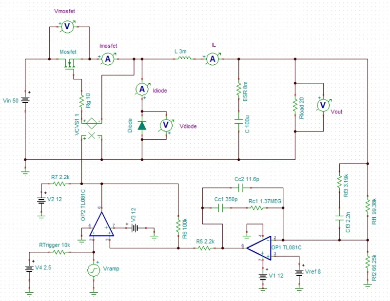
The following table shows the components used and their parameters for designing the above buck converter
| Sr. No. | Components | Parameters |
| 1 | DC Input Voltage Source | 50 V |
| 2 | Switching Inductor | 3 mH |
| 3 | Output Capacitor | 100 uF |
| 4 | Equivalent Series Resistance | `8 mOmega` |
| 5 | Load Resistance | `20 Omega` |
| 6 | Resistor `R_(f1)` | `99.381 kOmega` |
| 7 | Resistor `R_(f2)` | `66.254 kOmega` |
| 8 | Resistor `R_(f3)` | `3190 Omega` |
| 9 | Capacitor `C_(f3)` | 2.2 nF |
| 10 | Resistor `R_(c1)` | `1370.877 kOmega` |
| 11 | Capacitor `C_(c1)` | 0.35 nF |
| 12 | Capacitor `C_(c2)` | 11.6 pF |
| 13 | Reference Voltage | 8 V |
| 14 | Ramp Voltage | 2.5 V |
Results:
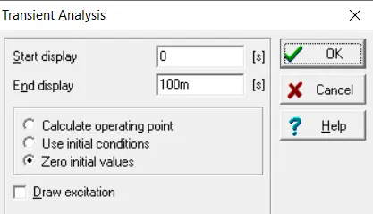
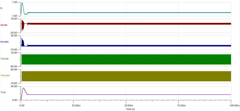
Carrying out the transient analysis as per the above figure, we get the following results
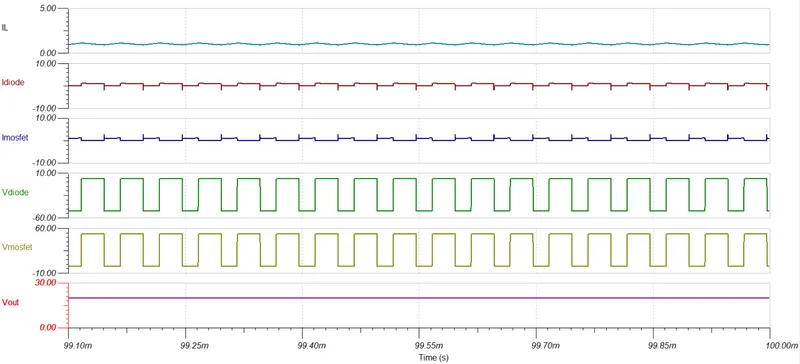
Zoomed-in:
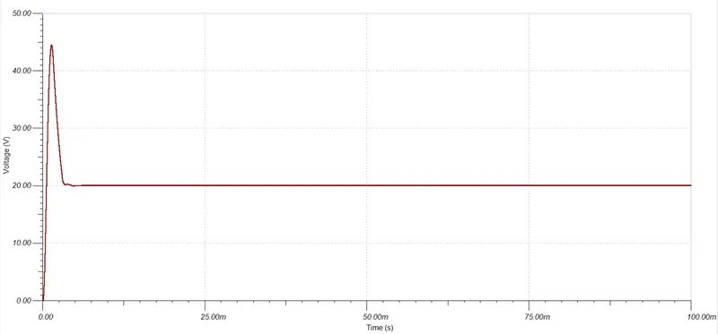
a. The output voltage transient and steady-state response:
Zoomed-in:
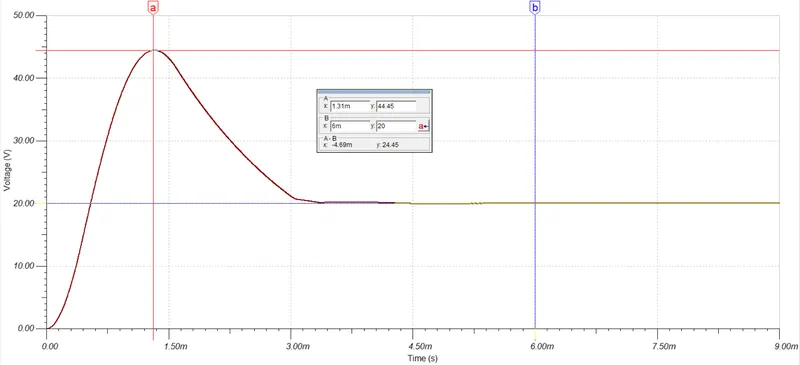
The output load voltage shoots up to a maximum of 44.45 V at the transient state and settles to a required steady-state value of 20 V in 6 msecs.
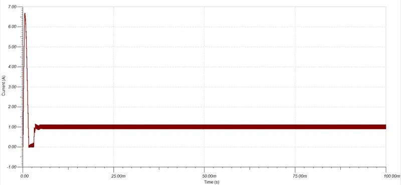
b. The Inductor Current:
Zoomed-in:
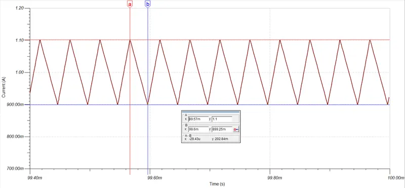
`I_(L(max)) = 1.1 A` and `I_(L(min)) = 0.899 A`
Therefore, the average inductor current = (1.1+0.899)/2 = 0.9995 A
And ripple in the inductor current = 1.1-0.899 = 0.201 A.
c. The Mosfet Current and Voltage:
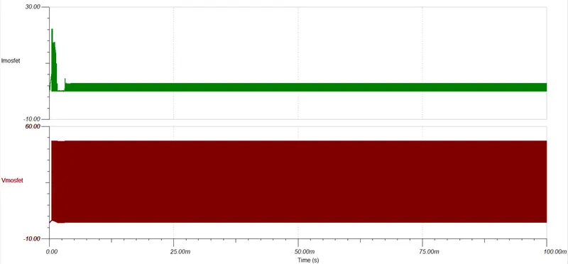
Zoomed-in:
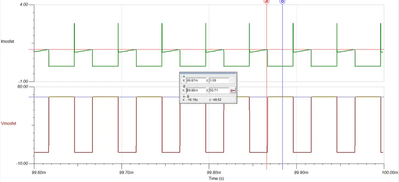
Mosfet Current = 1.09 A
Mosfet Peak Voltage = 50.71 V
d. The Diode Current and Voltage:
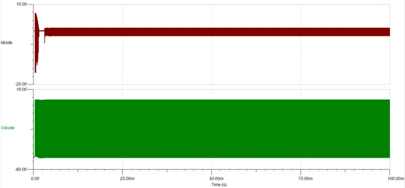
Zoomed-in:
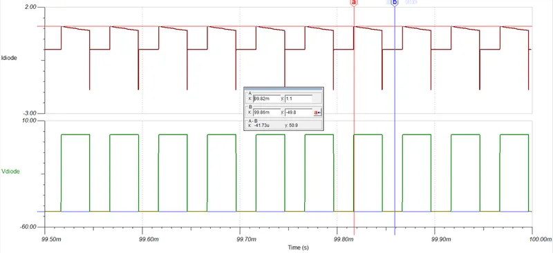
Diode Current = 1.1 A
Diode Inverse Peak Voltage = -49.8 V
Conclusion:
Thus, a buck converter with a voltage-control analog feedback circuit using a type III-B compensator is designed and simulated and the required output waveforms are obtained.
- Avinash S Paii am not getting the same result. please help