Design and simulation of full bridge rectifier using Boost converter as PFC
Aim: To design and simulate a single-phase full-wave bridge rectifier and achieve a unity power factor at different load ranges using a boost converter in Simulink.
Procedure:
A-
Given that:
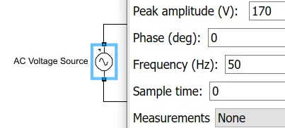
The peak amplitude of the AC voltage source (`V_m`) = 170 V
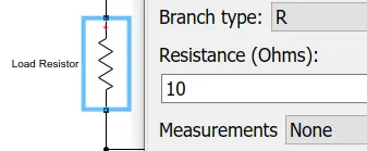
Load Resistance (R) = `10 Omega`
Calculations:
Assumptions:
Let the System frequency (F) = 50 Hz
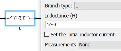
Filter Inductor (L) = 1 mH
We have to design a filter capacitor such that the output voltage ripple is less than 5%.
`therefore (DeltaV_o)/V_o = 0.05`
For a full-wave bridge rectifier, the filter capacitor is given by
`C = 1/(2F*R*((DeltaV_o)/V_o))`
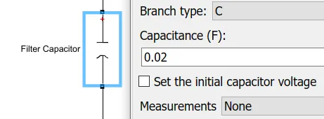
`therefore C = 1/(2*50*10*0.05) = 0.02 F`
This is the required capacitance value of the filter capacitor that will be used in the designed rectifier circuit.
B-
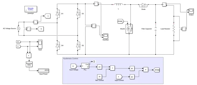
The following figure shows the designed model of a single-phase full-wave bridge rectifier using a boost converter as a power factor correction with a hysteresis control method
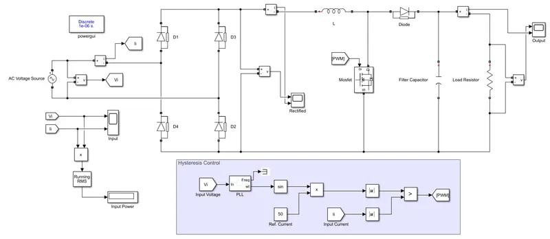
The conventional method of hysteresis control is known as the two-level hysteresis current control technique. It is a nonlinear method and it is based on current error. This method consists of a comparison between the input current and a band limit given to it. When it crosses the upper band limit, the switch turns off, when the current crosses the lower band limit, the switch turns on.
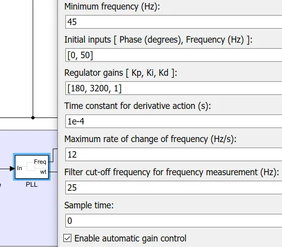
Here, the AC source voltage is first given to the PLL block. The PLL block models a Phase Lock Loop (PLL) closed-loop control system, which tracks the frequency and phase of a sinusoidal signal by using an internal frequency oscillator. The control system adjusts the internal oscillator frequency to keep the phase difference to 0. The output of this block is the angle (rad) varying between 0 and 2*pi, synchronized on the zero-crossing (rising) of the fundamental of the input signal. This angle output is then given to the Sin block and multiplied with the reference input current.
The absolutes of this acquired ref. current and the actual input current is then compared using a Relational Operator. This ref. current is the band limit, when the input current crosses the upper band limit, the switch turns off, and when the input current crosses the lower limit, the switch turns on. In this way, the PWM signals are generated and given to the Mosfet gate for the switching action.
The following are the components and their parameters used to design the above circuit
1. AC Source Voltage:
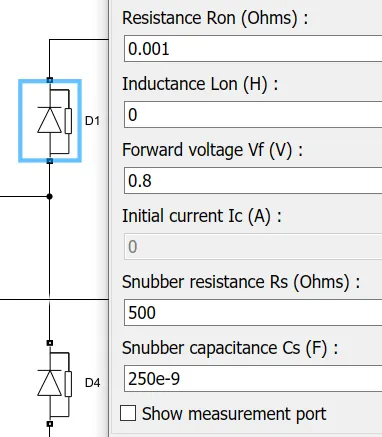
2. Diodes (bridge and boost circuit):
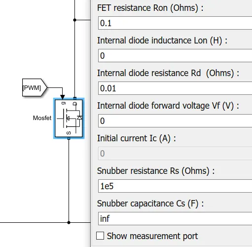
3. MOSFET:
4. Filter Inductor:
5. Filter Capacitor:
6. Load Resistor:
7. Phase Lock Loop:
Results:
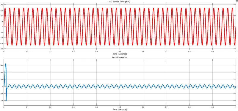
After running the simulation for 1 sec, we get the following output waveforms
a. Input Voltage and Current:
Zoomed-in:
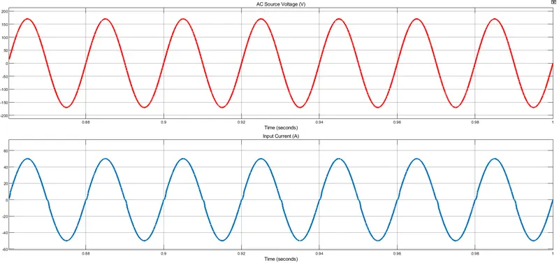
As we can observe from the zoomed-in results, the source voltage and the input current are in phase with each other and thus we can conclude that the unity power factor is achieved at the input stage.
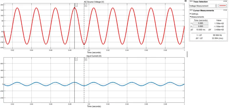
The input source voltage is a pure sinusoidal signal and the peak amplitude is 170 V as defined.
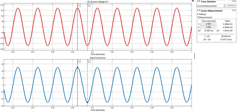
The input current is a sinusoidal signal and the peak amplitude is 50 A as defined in the reference voltage block.
b. Input Power:
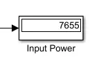
The RMS value of the input power is 7655 W.
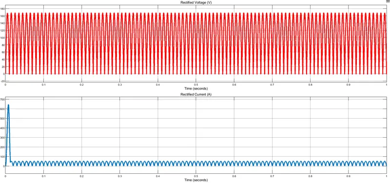
c. Rectified Voltage and Current:
Zoomed-in:
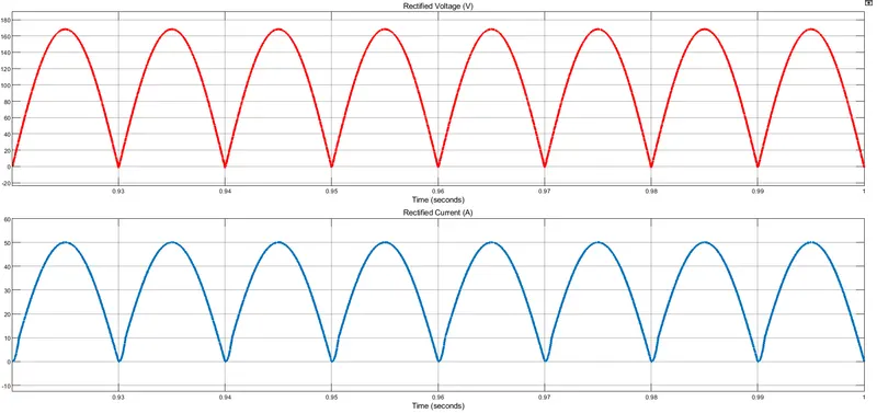
As we can observe from the zoomed-in results, the rectified voltage and the current are in phase with each other and thus we can conclude that the unity power factor is achieved after rectification.
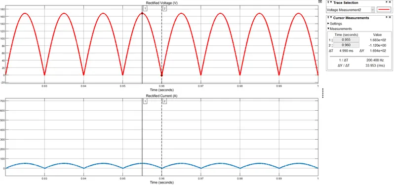
The rectified voltage is a pulsating DC voltage with a peak amplitude of 168.3 V.
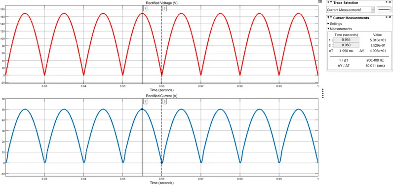
The rectified current is a pulsating DC with a peak amplitude of 50.1 A.
d. Output Load Voltage and Current:
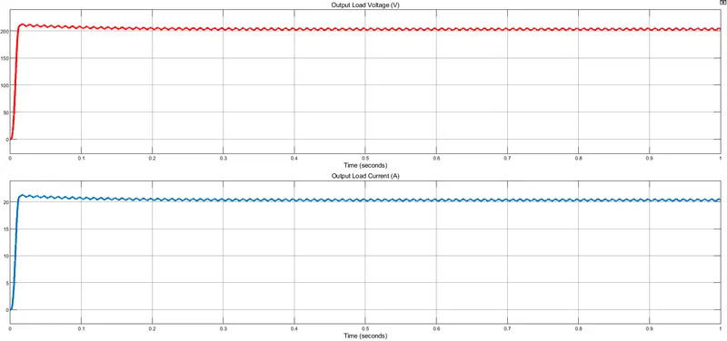
Zoomed-in:
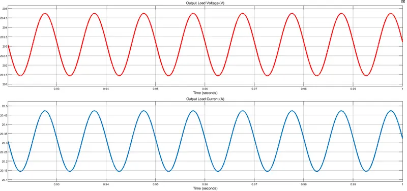
As we can observe from the zoomed-in results, the output load voltage and the current are in phase with each other and thus we can conclude that the unity power factor is achieved at the output stage.
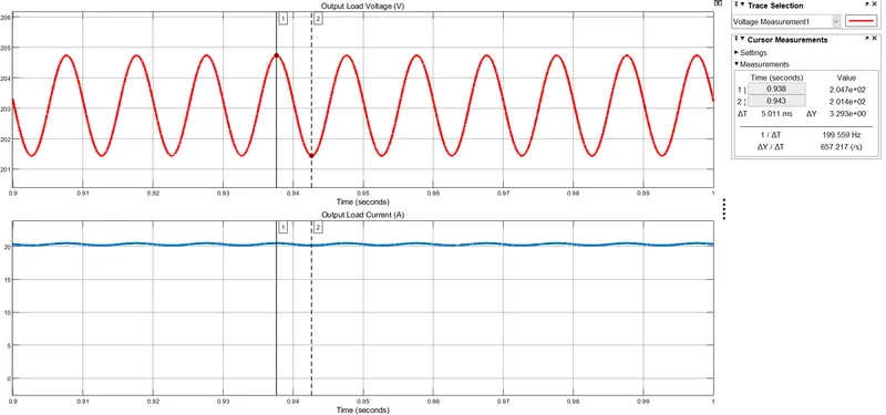
`V_(o(max)) = 204.7 V` and `V_(o(min)) = 201.4 V`
Therefore, the average output load voltage = (204.7+201.4)/2 = 203 V
The ripple in the output load voltage = 204.7-201.4 = 3.3 V
The ripple in the output load voltage is less than 5% of the average output load voltage. Thus, we can conclude that the filter capacitor is designed satisfactorily.
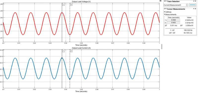
`I_(o(max)) = 20.47 A` and `I_(o(min)) = 20.14 A`
Therefore, the average output load current = (20.47+20.14)/2 = 20.3 A
The ripple in the output load current = 20.47-20.14 = 0.33 A.
| Sr. No. | Parameters | Simulated results |
| 1 | Source voltage peak amplitude | 170 V |
| 2 | Input current peak amplitude | 50 A |
| 3 | Input Power | 7655 W |
| 4 | Rectified voltage peak amplitude | 168.3 V |
| 5 | Rectified current peak amplitude | 50.1 A |
| 6 | Average output load voltage | 203 V |
| 7 | Average output load current | 20.3 A |
C-
Now, changing the reference input current to 65 A for obtaining a different input power range and simulating the model for 1 sec, we get the following output waveforms
a. Input Power:
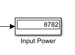
The RMS value of the input power is 8782 W.
b. Input Voltage and Current:
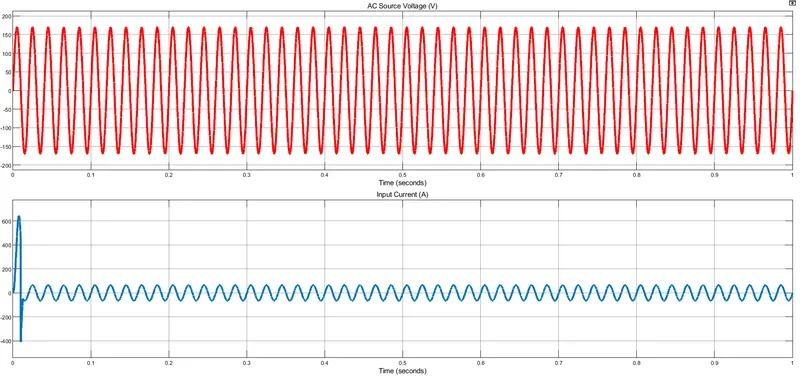
Zoomed-in:
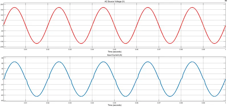
As we can observe from the zoomed-in results, the source voltage and the input current are in phase with each other and thus we can conclude that the unity power factor is achieved at the input stage.
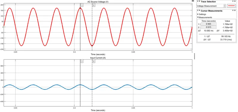
The input source voltage is a pure sinusoidal signal and the peak amplitude is 170 V as defined.
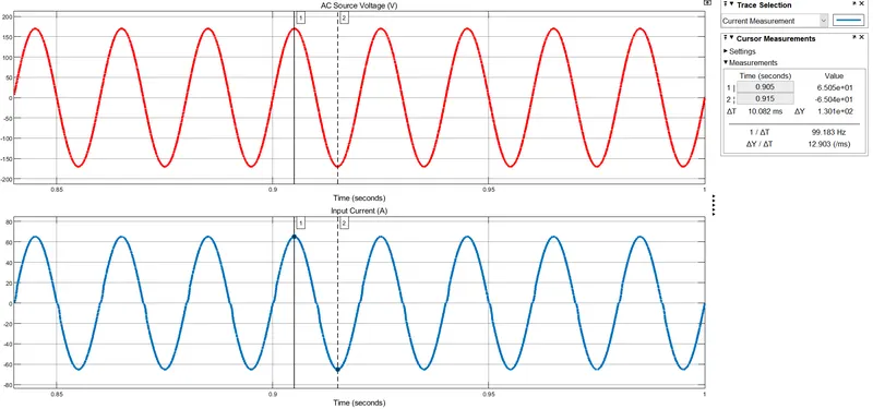
The input current is a sinusoidal signal and the peak amplitude is 65 A as defined in the reference voltage block.
c. Rectified Voltage and Current:
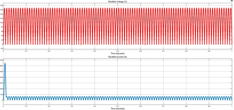
Zoomed-in:
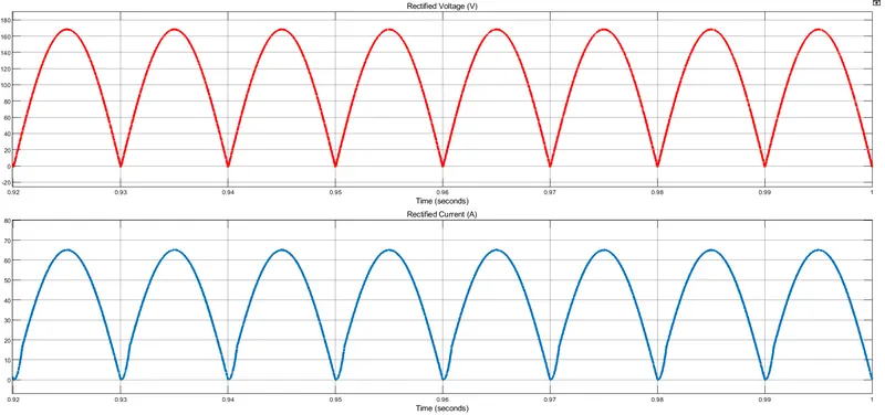
As we can observe from the zoomed-in results, the rectified voltage and the current are in phase with each other and thus we can conclude that the unity power factor is achieved after rectification.
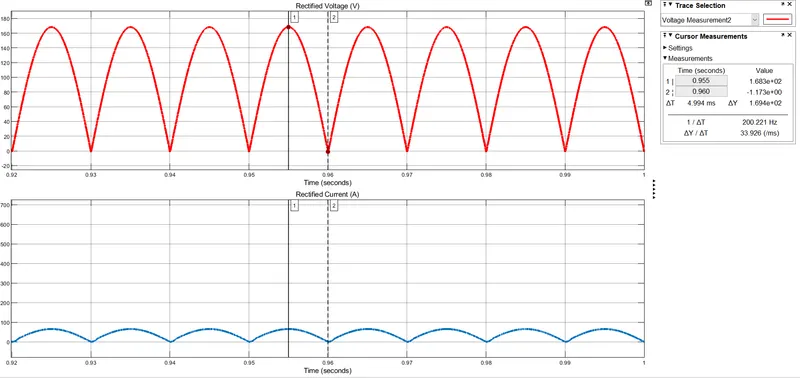
The rectified voltage is a pulsating DC voltage with a peak amplitude of 168.3 V.
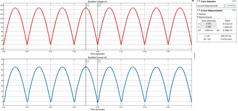
The rectified current is a pulsating DC with a peak amplitude of 65.14 A.
d. Output Load Voltage and Current:
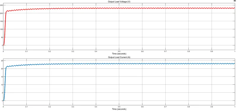
Zoomed-in:
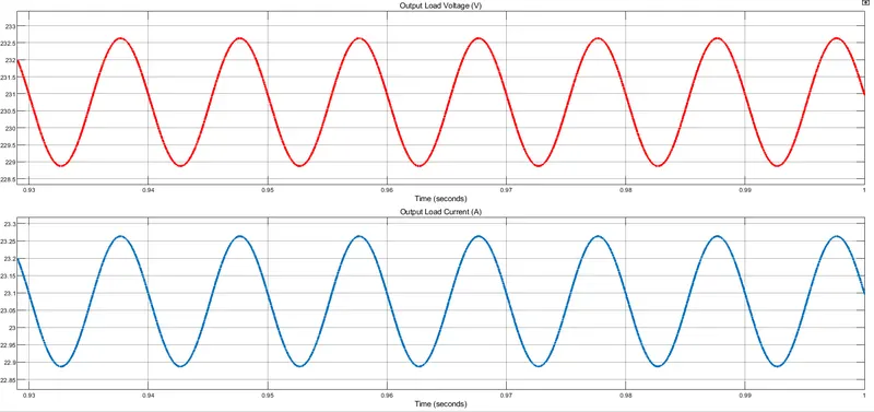
As we can observe from the zoomed-in results, the output load voltage and the current are in phase with each other and thus we can conclude that the unity power factor is achieved at the output stage.
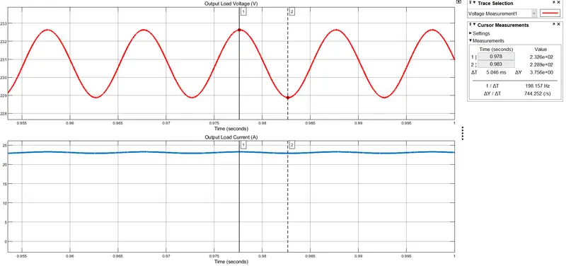
`V_(o(max)) = 232.6 V` and `V_(o(min)) = 228.9 V`
Therefore, the average output load voltage = (232.6+228.9)/2 = 230.75 V
The ripple in the output load voltage = 204.7-201.4 = 3.7 V
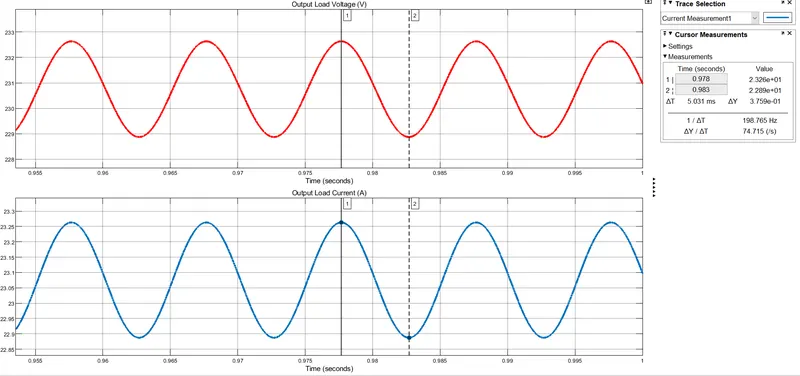
`I_(o(max)) = 23.26 A` and `I_(o(min)) = 22.89 A`
Therefore, the average output load current = (23.26+22.89)/2 = 23.075 A
The ripple in the output load current = 20.47-20.14 = 0.37 A.
| Sr. No. | Parameters | Simulated results |
| 1 | Source voltage peak amplitude | 170 V |
| 2 | Input current peak amplitude | 65 A |
| 3 | Input Power | 8782 W |
| 4 | Rectified voltage peak amplitude | 168.3 V |
| 5 | Rectified current peak amplitude | 65.14 A |
| 6 | Average output load voltage | 230.75 V |
| 7 | Average output load current | 23.075 A |
D-
After many simulations with different reference currents, I've found that the minimum power flow that is allowed in the rectifier with the chosen components where the input current is sinusoidal in nature has a constant magnitude, works in continuous conduction mode, and is in phase with the source voltage throughout the simulation period is 6701 W with 35 A as a reference current.
The following figure shows the designed model of a single-phase full-wave bridge rectifier using a boost converter as a power factor correction with a hysteresis control method having 35 A as a reference current
After running the simulation for 1 sec, we get the following input current waveform
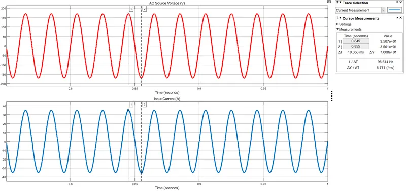
As we can observe, the input current is sinusoidal in nature, is in phase with the source voltage, works in continuous conduction mode, and have a constant peak amplitude of 35 A throughout the simulation period.
Below this current level, i-e, if the reference current is set at 30 A the magnitude of the current varies after sometime and starts to go out of phase. The following output waveform of the input current will justify that.
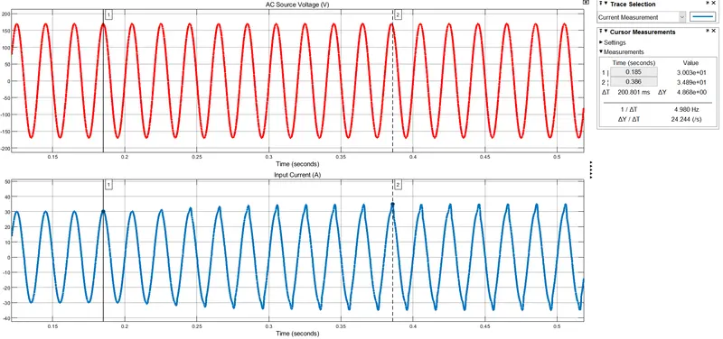
If we decrease the reference current more further, the sinusoidal waveform will get more and more deformed and will go into discontinuous conduction mode with a lesser conduction period.
Additional-
The following figure shows the designed model of a single-phase full-wave bridge rectifier using a boost converter as a power factor correction with a closed-loop feedback system
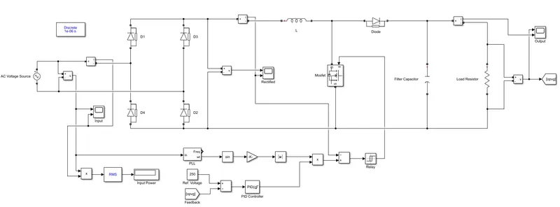
Choosing Output Load Voltage (`V_o`) = 250 V ...(Since a boost converter is used, the output load voltage will be greater than the source voltage)
In this designed model the output voltage is taken as feedback and compared with the reference voltage which is 250 V (desired), the error signal is then given to the PI controller and then multiplied by the absolute value of the sine of the angle of the source voltage given by the PLL block used. It is then compared with the rectified current to match the phases and the resulting output is the PWM signal required for the switching action of the Mosfet passed via a Relay block.
The following figure shows the tracking of output load voltage after simulating the model for 1 sec
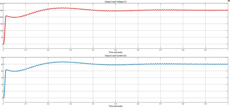
Zoomed-in:
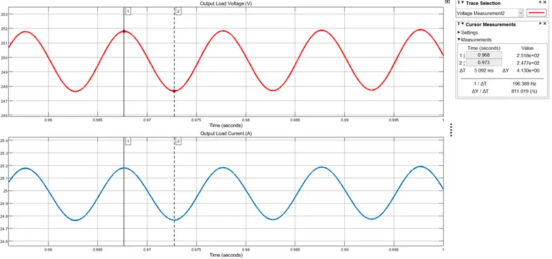
As we can observe, the average value of the output load voltage is 250 V with a ripple of less than 5%.
As it is a closed-loop design, the system will track the output voltage according to the reference voltage provided as long as it is in the limits as per the designed circuit and its components.
Conclusion:
Thus, the design and simulation of a single-phase full-wave bridge rectifier using a boost converter as a power factor correction is performed satisfactorily.