Interleaving Forward Converter
Aim: To design an interleaving DC/DC converter system for a data center application.
Procedure:
Design specifications:
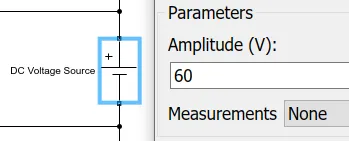
Input Voltage (`V_i`) = 60 V
Output Voltage (`V_o`) = 3 V
Output Current (`I_o`) = 100 A
Efficiency > 85%
Calculations:
Choosing an interleaved forward converter for the given application.
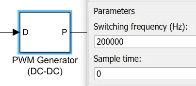
Assuming the Duty ratio to be 50% and the Switching frequency to be 200 kHz.
We know that the Voltage ratio for a forward converter is
`V_o/V_i = D*N_2/N_1`
`therefore N_2/N_1 = V_o/V_i*1/D`
`therefore N_2/N_1 = 3/60*1/0.5 = 1/10`
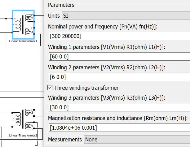
Hence, choosing N1 = 60 turns and N2 = 6 turns.
Due to the design restrictions
`D(1+N_3/N_1) < 1`
`therefore 0.5(1+N_3/60) < 1`
`therefore N_3 < 60`
Hence, choosing N3 = 30 turns.
Load Resistance (R) = `V_o/I_o`
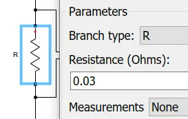
`therefore R = 3/100 = 0.03 Omega`
Output Power (`P_o`) = `V_o^2/R`
`therefore P_o = 3^2/0.03 = 300 W`
Total Inductance Current (`I_L`) = `V_o/R`
`I_L = 3/0.03 = 100 A`
Total Inductance Current (`I_L`) = `I_(L1)+I_(L2)`
Since we are considering both the filter inductor to have the same inductance, i-e, `L_(X1)=L_(X2)`
Therefore, `I_(L1)=I_(L2)`
`therefore I_L = 2I_(L1) = 2I_(L2)`
Hence, `I_(L1) = I_(L2) = 50A`
Designing both the filter inductors for 10% ripple in the inductor current.
`DeltaI_(L1) = DeltaI_(L2) = 0.1*I_(L1)`
`therefore DeltaI_(L1) = DeltaI_(L2) = 0.1*50 = 5 A`
The inductance of the filter inductor is given by
`L_1 = L_2 = V_o/(f_sDeltaI_(L1))(1-D)`
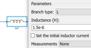
`L_1 = L_2 = 3/(200000*5)(1-0.5) = 1.5 muH`
Designing the output Capacitor for 5% ripple in the output voltage.
`DeltaV_o = 0.05*V_o`
`therefore DeltaV_o = 0.05*3 = 0.15 V`
The Capacitance of the output Capacitor is given by
`C = (1-D)/(8Lf_s^2((DeltaV_o)/V_o))`
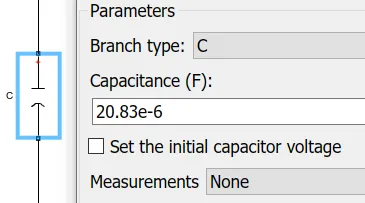
`therefore C = (1-0.5)/(8*1.5*10^-6*200000^2*0.05) = 20.83 muF`
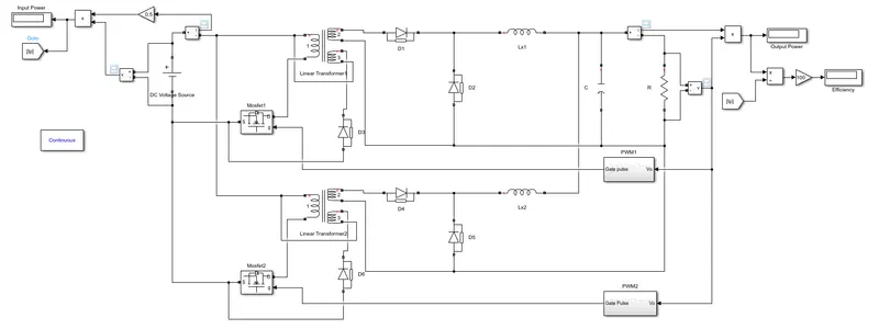
The following figure shows the designed model of an interleaved forward converter using Simulink
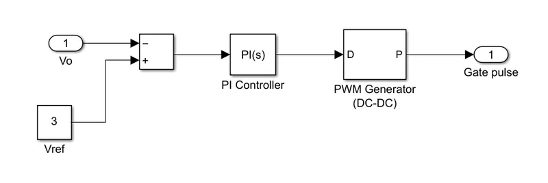
PWM and Control subsystem for MOSFET1:
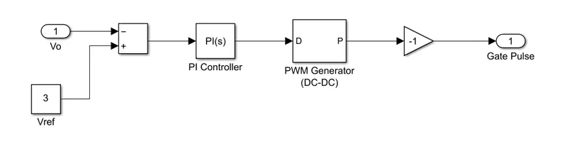
For MOSFET2:
The following are the components and their parameters used to design the above interleaved forward converter
1. DC Voltage Source:
2. Linear Transformers:
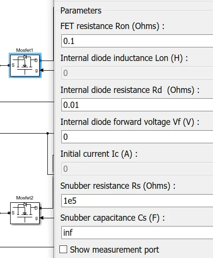
3. MOSFETs:
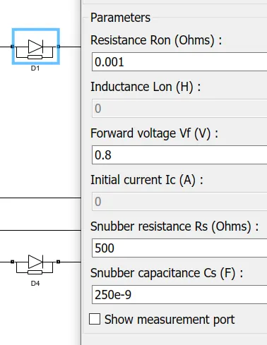
4. Diodes:
5. Filter Inductors (Lx1 and Lx2):
6. Output Capacitor:
7. Load Resistor:
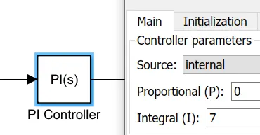
8. PI Controller:
9. PWM Generator:
Results:
After simulating the designed converter for 0.5 secs, we get the following required output waveform results
a. Input Voltage and Current:
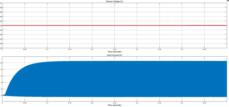
Input voltage is a constant 60 V supply.
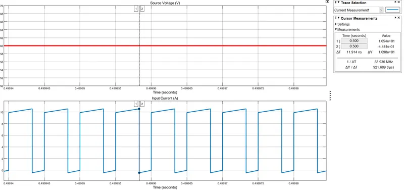
`I_(i(max)) = 10.54 A` and `I_(i(min)) = -0.44 A`
Therefore, the average input current = (10.54+(-0.44))/2 = 5.05 A
The ripple in the input current = 10.54-(-0.44) = 10.98 A
b. Output Voltage and Current:
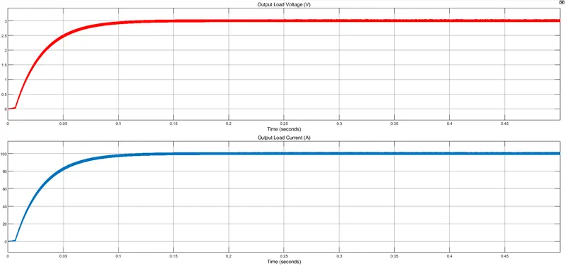
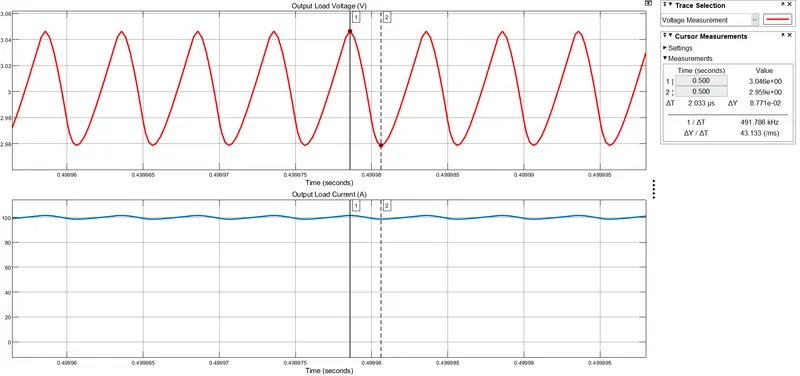
`V_(o(max)) = 3.046 V` and `V_(o(min)) = 2.959 V`
Therefore, the average output load voltage = (3.046+2.959)/2 = 3.0025 V
The ripple in the output load voltage = 3.046-2.959 = 0.087 V
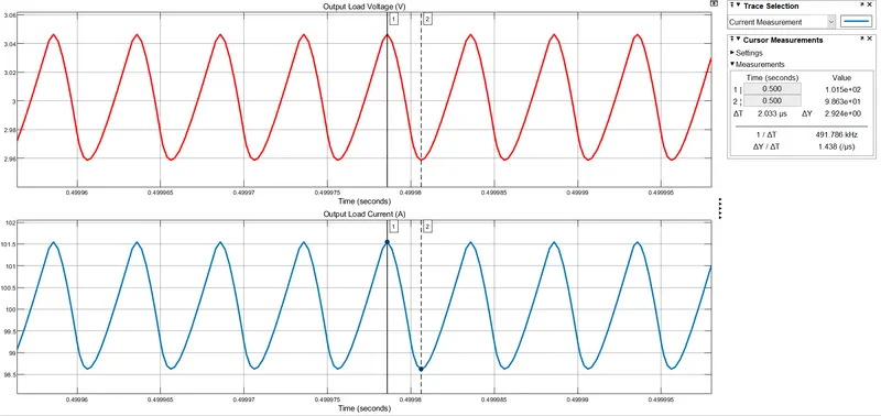
`I_(o(max)) = 101.5 A` and `I_(o(min)) = 98.63 A`
Therefore, the average output load current = (101.5+98.63)/2 = 100.065 A
The ripple in the output load current = 101.5-98.63 = 2.87 A
c. Input Power:
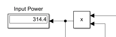
The input power is 314.4 W.
d. Output Power:
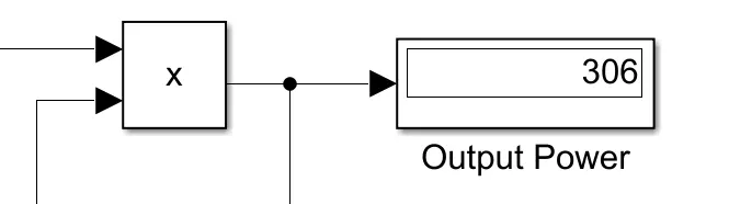
The output power is 306 W.
e. Efficiency:
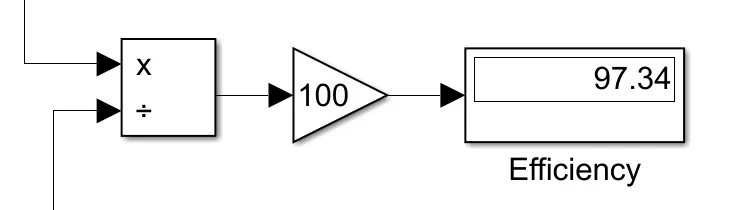
The efficiency of the designed converter = Output power/ Input power *100 = 97.34%.
Hence, the designed converter works very efficiently.
Conclusion:
The designed interleaved forward converter for the data center application works efficiently and provides the required output waveforms satisfactorily.