Design of a Closed-Loop Boost Converter
Aim: To design and simulate a closed-loop Boost converter in continuous conduction mode using Simulink.
Procedure:
1-
Given that:
Varying source voltage = 200-300 V
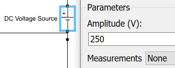
Therefore, average source voltage (`V_i`) = (200+300)/2 = 250 V
Output load voltage (`V_o`) = 400 V
Power level (P) = 4 kW
Calculations:
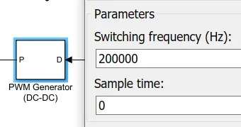
It's a high-power system, so assuming the switching frequency to be 200 kHz.
Load Resistance (R) = `V_o^2/P`
`therefore R = 400^2/4000 = 40 Omega`
The voltage ratio of a boost converter is given by
`V_o/V_i = 1/(1-D)`
When source voltage = 200 V
`400/200 = 1/(1-D)`
`therefore D = 0.5`
When source voltage = 300 V
`400/300 = 1/(1-D)`
`therefore D = 0.25`
Therefore, the range of the duty ratio of the boost converter is 0.25-0.5 i-e 25% to 50%.
Taking average source voltage = 250 V
`400/250 = 1/(1-D)`
`therefore D = 0.375`
Hence, considering the duty ratio of 0.375 or 37.5% for further calculations.
Inductor current (`I_L`) = `V_i/((1-D)^2*R)`
`therefore I_L = 250/((1-0.375)*40) = 16 A`
Now, designing for less than 10% ripple of the average inductor current
`DeltaI_L = 0.1*I_L`
`therefore DeltaI_L = 0.1*16 = 1.6 A`
The inductance in the switching inductor is given by
`L = V_i/(f_sDeltaI_L)*D`
`therefore L > 250/(200000*1.6)*0.375`
`therefore L > 0.2929 mH`
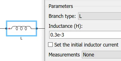
Hence, choosing L = 0.3 mH
This inductor of 0.3 mH will pass the current with less than 10% ripples.
Now, designing for less than 1% ripple of the average output voltage
`DeltaV_o = 0.01*V_o`
`therefore DeltaV_o = 0.01*400 = 4 V`
The capacitance in the output capacitor is given by
`C = D/(Rf_s((DeltaV_o)/V_o))`
`therefore C > 0.375/(40*200000*(4/400))`
`therefore C > 4.6875 muF`
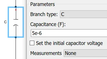
Hence, choosing `C = 5 muF`
This Capacitor of 5 uF will help in maintaining the output load voltage under 1% ripple.
2-
Gate driver:
For the designed boost converter, choosing UCC27511A-Q1 Single-Channel High-Speed Low-Side Gate Driver for controlling the switching operations of the Mosfet. The following figure shows the UCC27511A-Q1 gate driver with the non-inverting input operation
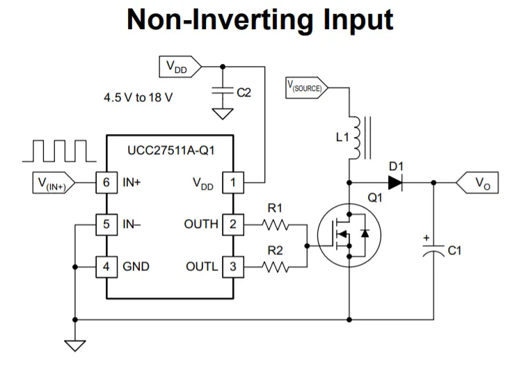
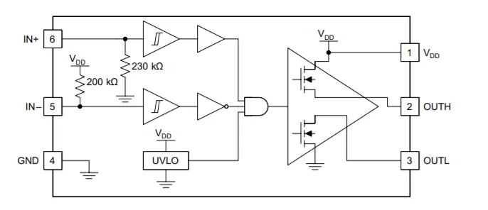
The term OUT refers to the combined state that results when the OUTH pin is tied directly to the OUTL pin. Output high, or OUT high refers to the state when the OUTH pin is pulled close to VDD pin bias voltage while the OUTL pin is in the high-impedance state. Similarly, output low or OUT low implies that the OUTL pin is pulled close to the GND pin while the OUTH pin is in the high-impedance state.
The figure below shows the internal functional block diagram of the UCC27511A-Q1 gate driver
RC network:
The following figure shows the type-III compensation network used for the designed boost converter
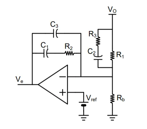
Calculations for the RC compensation network are as follows
Assuming the crossover frequency to be 1/5 of the switching frequency
`F_o = 1/5*f_s`
`therefore F_o = 1/5*200000 = 40000 = 40 kHz`
The compensator poles and zeros are chosen `70^o` phase lead at the crossover frquency.
Now, calculating poles and zeros of the compensator
`F_(Z2) = F_osqrt((1-sintheta)/(1+sintheta))`
`therefore F_(Z2) = 40000sqrt((1-sin70^o)/(1+sin70^o)) = 7053.079 Hz`
`F_(P2) = F_osqrt((1+sintheta)/(1-sintheta))`
`therefore F_(P2) = 40000sqrt((1+sin70^o)/(1-sin70^o)) = 226.85 kHz`
`F_(Z1) = 0.5*F_(Z2)`
`therefore F_(Z1) = 0.5*7053.079 = 3526.51 Hz`
And, `F_(P3) = F_s/2`
`therefore F_(P3) = 200000/2 = 100000 = 100 kHz`
Now, calculating the values of the parameters of the compensator
Choosing `C_2` = 2.2 nF
`R_3 = 1/(2pi*C_2*F_(P2))`
`therefore R_3 = 1/(2pi*2.2*10^-9*226.85*10^3) = 318.9 Omega`
Choosing `R_3 = 320 Omega`
`R_1 = 1/(2pi*C_2*F_(Z2))`
`therefore R_1 = 1/(2pi*2.2*10^-9*7053.079) = 9938.075 Omega`
Choosing `R_1 = 9.938 kOmega`
`R_b = (R_1*V_(ref))/(V_o-V_(ref))`
`R_b = (9938*80)/(400-80) = 2484.5 Omega`
Choosing `R_b = 2.485 kOmega`
`R_2 = (2pi*F_o*L*C*V_(osc))/(V_i*C_2)`
`therefore R_2 = (2pi*40000*0.3*10^-3*5*10^-6*400)/(250*2.2*10^-9) = 274175.358 Omega`
Choosing `R_2 = 274.175 kOmega`
`C_1 = 1/(2pi*R_2*F_(Z1))`
`therefore C_1 = 1/(2pi*274175*3526.51) = 164.6 pF`
Choosing `C_1 = 164 pF`
`C_2 = 1/(2pi*R_2*F_(P3))`
`therefore C_2 = 1/(2pi*274175*100000) = 5.804 pF`
Choosing `C_2 = 5.8 pF`
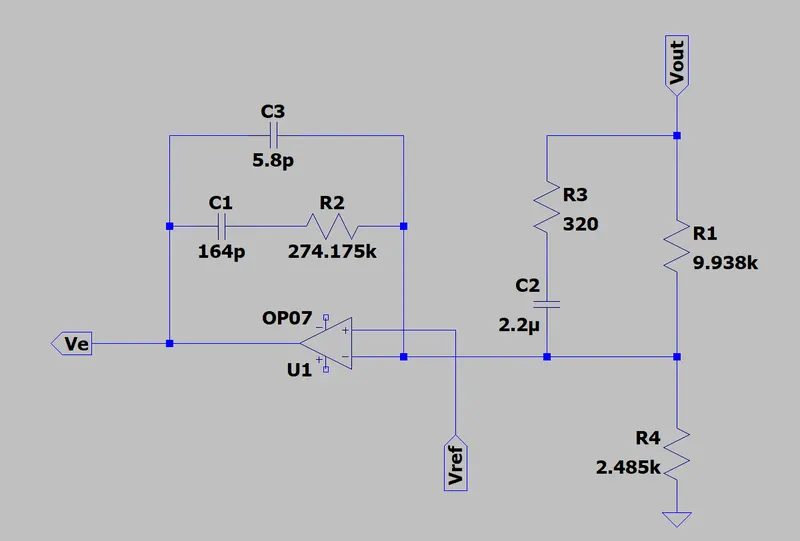
The following figure shows the designed RC compensation network
3-
The following figure shows the designed model of a closed-loop boost converter using Simulink
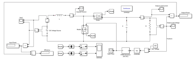
The following are the components and their parameters used to design the above closed-loop boost converter
1. DC voltage source:
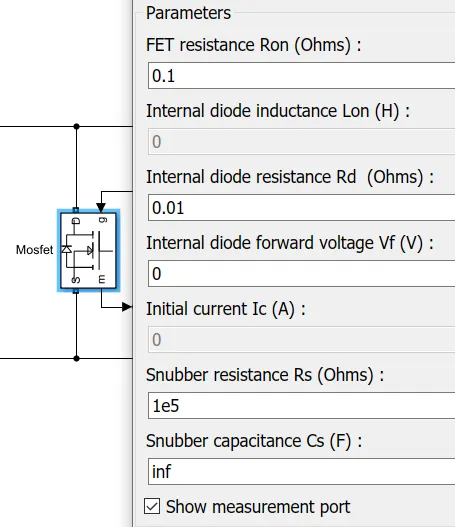
2. MOSFET:
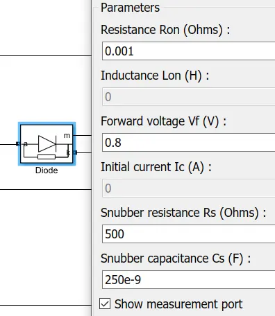
3. Diode:
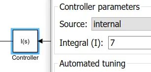
4. Controller:
5. PWM Generator:
6. Switching Inductor:
7. Output Capacitor:
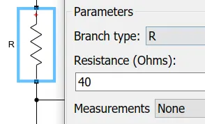
8. Load Resistor:
Results:
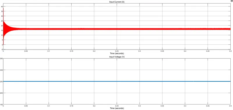
After running the simulation for 0.5 secs, we get the following output waveforms
a. Input Current and Voltage:
Zoomed-in:
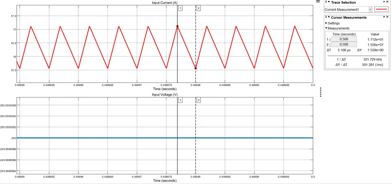
`I_(i(max)) = 17.12 A` and `I_(i(min)) = 15.56 A`
Therefore, the average input current = (17.12+15.56)/2 = 16.34 A
The ripple in the input current = 17.12-15.56 = 1.56 A
And, the input voltage is a constant 250 V supply.
b. Input Power:
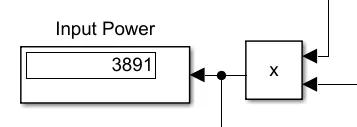
The input power is the product of the input voltage and current.
Hence, the input power of the designed converter is 3891 W.
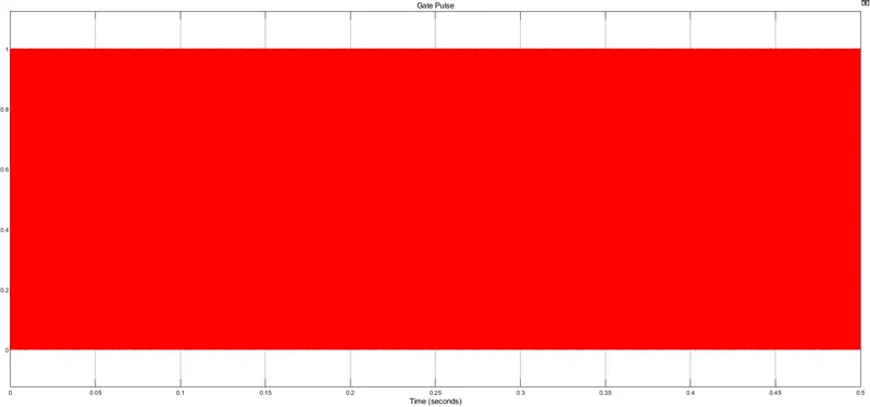
c. Gate Pulse:
Zoomed-in:
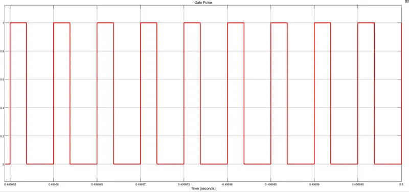
As the duty ratio calculated was 0.375 or 37.5%, the PWM generator is generating the gate pulse of 37.5% turn ON period of the one whole cycle to trigger the Mosfet.
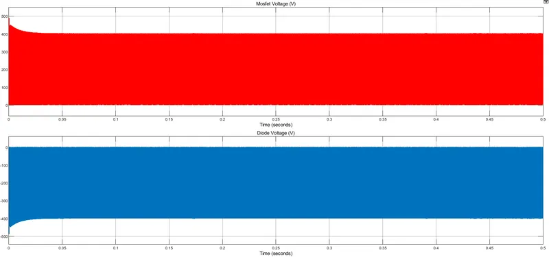
d. Mosfet and Diode Voltages:
Zoomed-in:
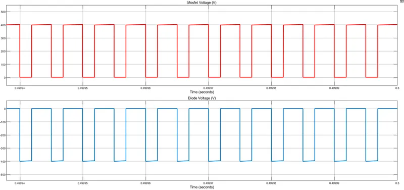
The peak Mosfet voltage = 400 V
The peak inverse Diode voltage = -400 V
e. Inductor Current:
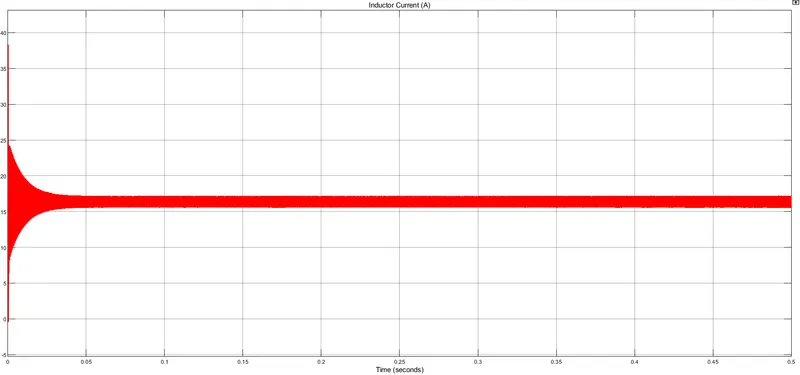
Zoomed-in:
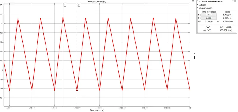
`I_(L(max)) = 17.12 A` and `I_(L(min)) = 15.56 A`
Therefore, the average inductor current = (17.12+15.56)/2 = 16.34 A
The ripple in the inductor current = 17.12-15.56 = 1.56 A
f. Output Load Current:
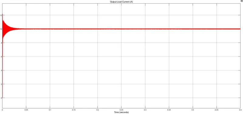
Zoomed-in:
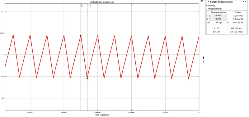
`I_(o(max)) = 10.04 A` and `I_(o(min)) = 9.946 A`
Therefore, the average output load current = (10.04+9.946)/2 = 9.993 A
The ripple in the inductor current = 10.04-9.946 = 0.094 A
g. Output Load Voltage:
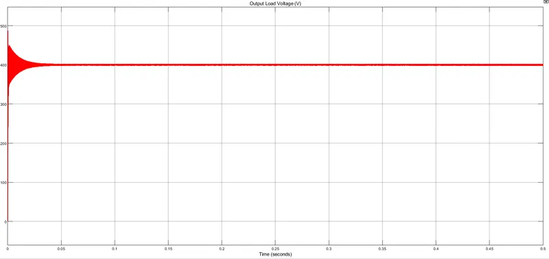
Zoomed-in:
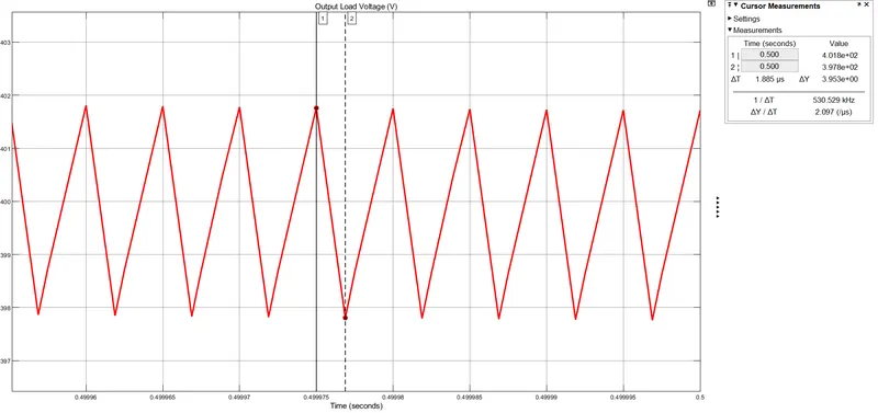
`V_(o(max)) = 401.8 V` and `V_(o(min)) = 397.8 V`
Therefore, the average output load voltage = (401.8+397.8)/2 = 399.8 V
The ripple in the output load voltage = 401.8-397.8 = 4 V
h. Output Power:
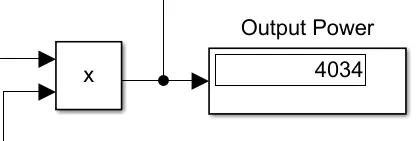
The output power is the product of the output load voltage and current.
Hence, the output power of the designed converter is 4034 W.
i. Efficiency:
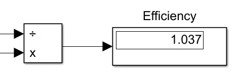
Efficiency is the division of output power by input power.
Hence, the efficiency of the designed converter is 1.037 or 103.7%.
The efficiency of the designed converter is high due to the closed-loop feedback circuit and the controller which maintains the output load voltage to be equal or near to the reference voltage provided.
j. The designed converter is a closed-loop system which means it can provide output load voltages at different levels up to certain limitations.
So let's test the system ability at different dynamic conditions of the designed converter.
Now, setting the reference voltage at 350 V and then simulating again, we get the following output load voltage waveform
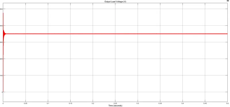
Zoomed-in:
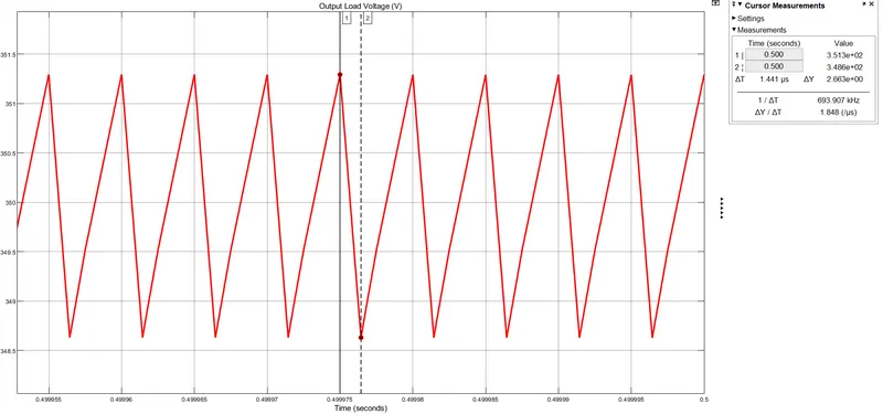
`V_(o(max)) = 351.3 V` and `V_(o(min)) = 348.6 V`
Therefore, the average output load voltage = (351.3+348.6)/2 = 349.95 V
The ripple in the output load voltage = 351.3-348.6 = 2.7 V
Hence, the system is tracking the reduced output voltage satisfactorily with a lesser output voltage ripple.
| Sr. no. | Parameters | Simulated results |
| 1 | Input Current | 16.34 A |
| 2 | Input Voltage | 250 V |
| 3 | Input Power | 3891 W |
| 4 | Peak Mosfet Voltage | 400 V |
| 5 | Peak Inverse Diode Voltage | -400 V |
| 6 | Inductor Current | 16.34 A |
| 7 | Output Load Current | 9.993 A |
| 8 | Output Load Voltage | 399.8 V |
| 9 | Output Power | 4034 W |
| 10 | Efficiency | 103.7% |
4-
Specifications of components used in the circuit:
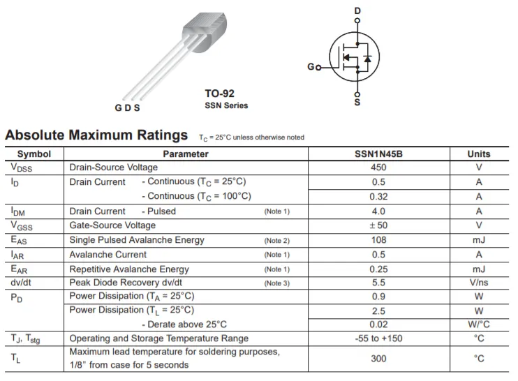
1. MOSFET:
SSN1N45B 450V N-Channel MOSFET can be used in this circuit.
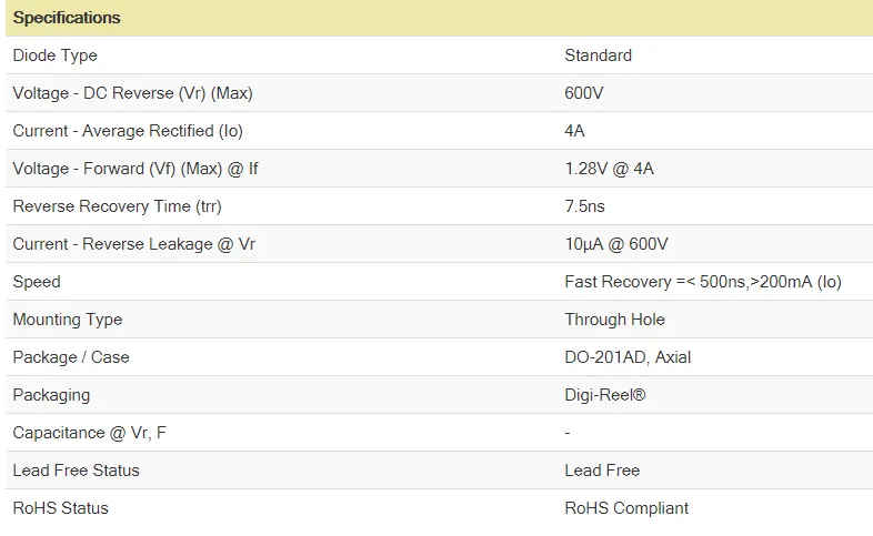
2. Diode:
MUR460-E3/54 fast recovery Diode can be used in this circuit.
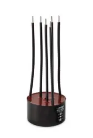
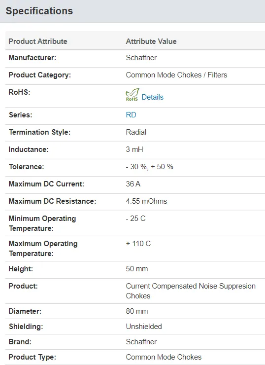
3. Switching Inductor:
RD8127-36-3M0 current compensated inductor can be used in this circuit.
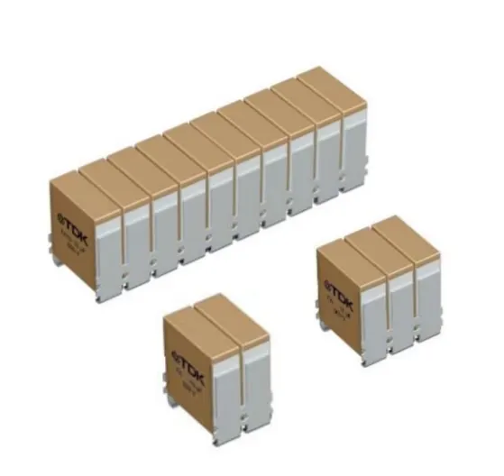
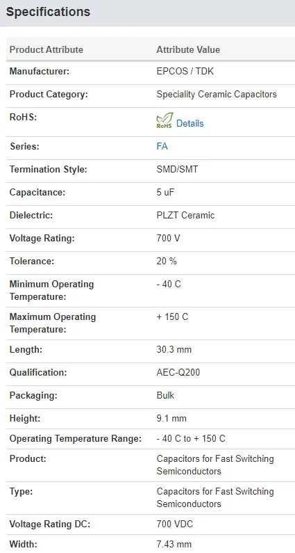
4. Capacitor:
B58035U7505M001 ceramic capacitor can be used in this circuit.
Conclusion:
Thus, the simulation is performed for the closed-loop boost converter and a design report is made with components specifications.