Week 9 - PCB Thermal Simulation
Theory:
Electronic components generate heat energy and dissipate a significant amount onto PCBs. Thermal management techniques such as heat sinks are often used to accelerate the heat dissipation rate from the electronic component to the ambient. Heat sinks offer low thermal resistance from the junction to the case and case to ambient, thus facilitating heat transfer. While specifying the heat sink for the electronic component of interest, heat energy dissipation through the PCB becomes significant. The thermal properties of a PCB are critical to the operating junction temperature of the component. The thermal conductivity property of PCBs is even more critical with the proliferation of high power density and high-speed electronic circuit design.
- The thermal properties of a PCB are critical to the operating junction temperature of a component.
- To predict the heat transfer to the PCB, PCBs are modeled as a single unit with two effective thermal conductivities: effective parallel thermal conductivity and effective normal thermal conductivity.
- The effective parallel and normal thermal conductivities of a PCB are dependent on the total thickness of the PCB as well as the thickness of the layers of copper and glass-epoxy.
Thermal Conductivity of PCBs
PCBs are layered structures consisting of copper foils and glass-reinforced polymers that connect components electrically and support them mechanically using pads, conductive traces, and vias. High thermal conductivity copper foils are sandwiched between low thermal conductivity glass-epoxy layers. The copper forms the conductive circuit in a PCB, whereas glass-epoxy layers are the non-conductive substrate.
Conductive Materials
The most commonly used conductive material is copper. Other options include aluminium, chrome, and nickel. The non-conductive substrate most commonly used is FR-4 laminate. The thermal conductivity of copper is about 400 W/m/K and the thermal conductivity of FR-4 is 0.2 W/m/K. The copper acts as a thermal conductor and the laminate acts as a thermal insulator. There is a vast difference between the thermal conductivity of copper and FR-4, and this makes the effective thermal conductivity of the PCB anisotropic.
Objective:
A PCB board, library files, and traces are imported to create the model. The model is first solved for conduction only, without the components and then solved using the actual components with forced convection.
Conduction model:
Modeling: Files are provided with this
- Create a new project
- Import board layout *.bdf & *.ldf (The board and the associated library files have to be chosen at this step and the trace file can be imported later.)
- Form the nonconformal assembly
- Import ECAD file (*.anf) A1.anf can be found in the folder containing the input files downloaded for his tutorial.
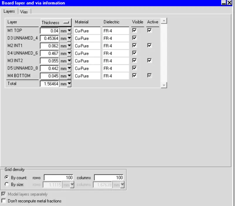
- Once the import process is completed, you can edit the layer information in the Board layer and via information panel (metal layers are pure Cu and the dielectric layers are FR-4.)
- Enter the layer thickness as shown in the table below.
|
Layer No. |
Layer Thickness (mm) |
|
1 |
0.04 |
|
2 |
0.45364 |
|
3 |
0.062 |
|
4 |
0.467 |
|
5 |
0.055 |
|
6 |
0.442 |
|
7 |
0.045 |
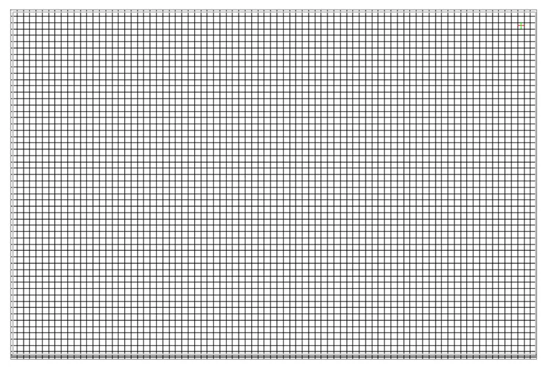
- Specify Grid density by size (0.508 mm X 0.508 mm)
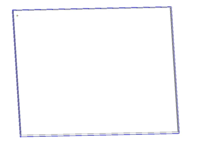
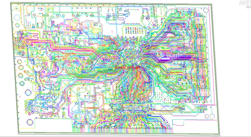
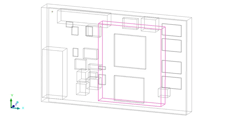
PCB model from the board file
Importing the board layer thickness and via layer information:
Metal fraction:
Trace by single colour
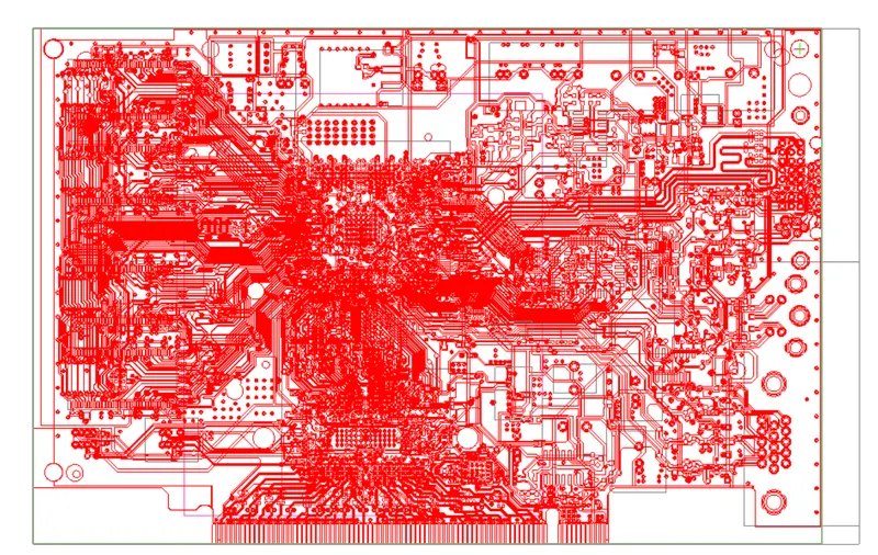
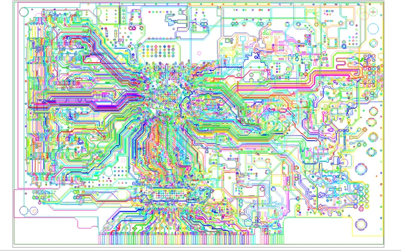
Trace by layer
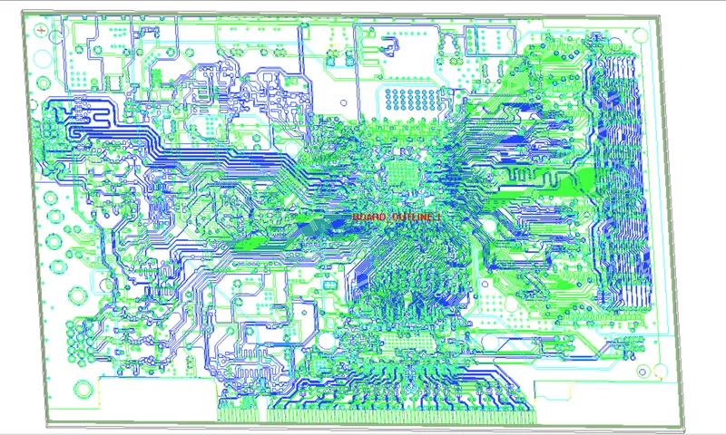
Trace by colour
Mesh settings:
Mesh of board PCB file
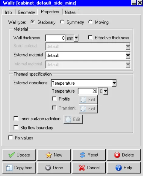
Cabinet inlet wall BC
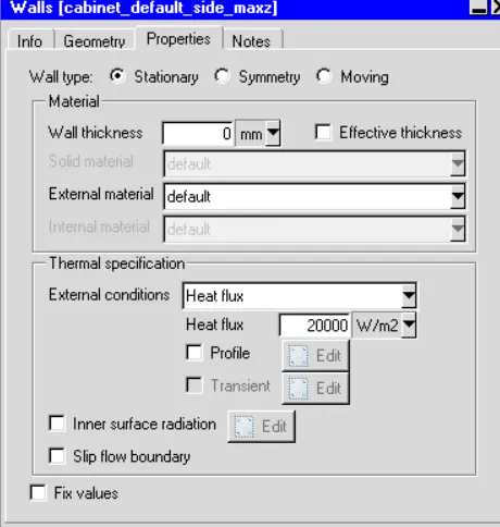
Cabinet outlet wall BC
Boundary condition:
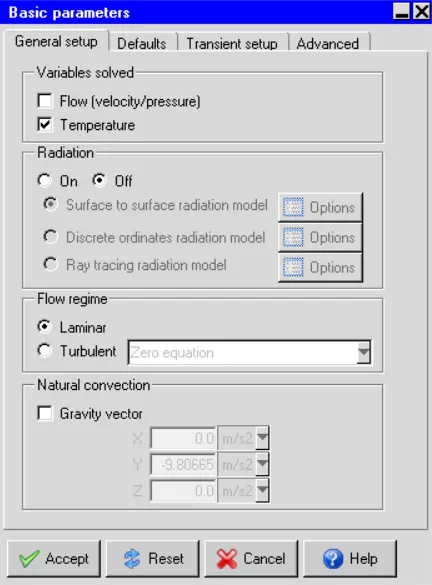
Basic parameter
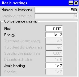
Convergence parameter
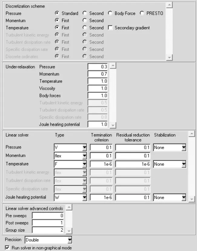
Advanced settings:
Post processing:
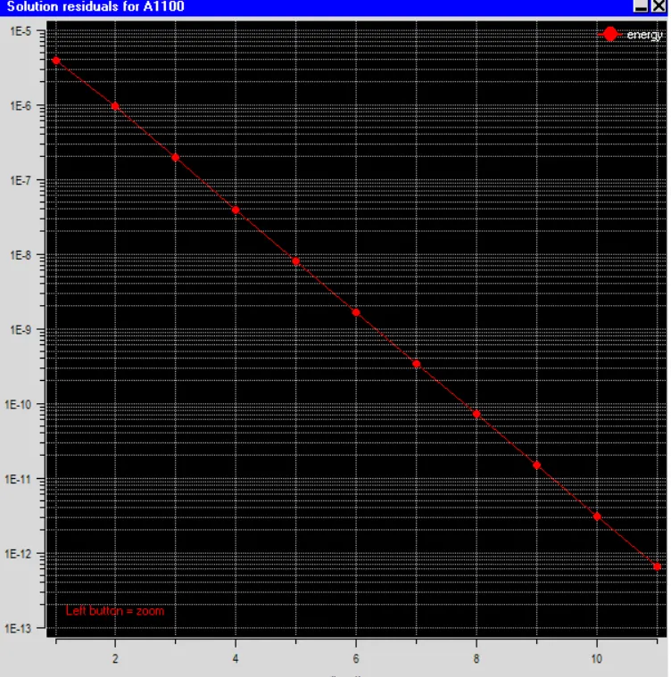
Iteration convergence
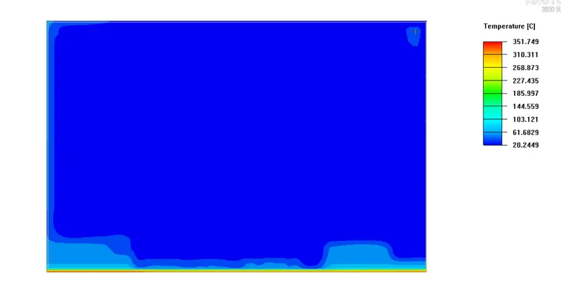
Temperature contour
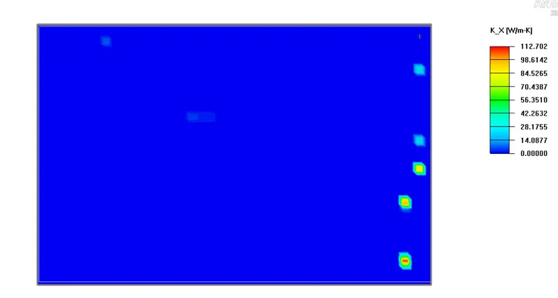
Conductivity in x direction
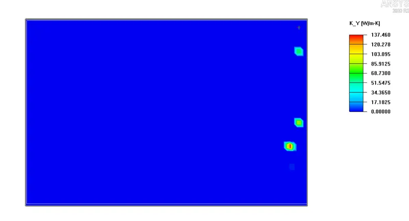
Conductivity in y direction
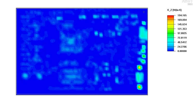
Conductivity in z direction
The temperature contour shows the thermal gradient from 351 degree C to 20 degree C. The temperature at the base of board is found to be maximum and the minimum at the other areas.
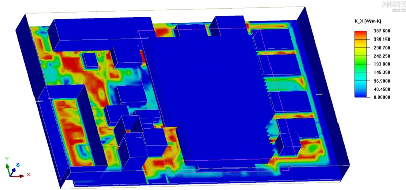
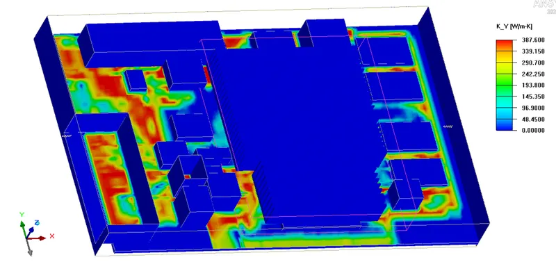
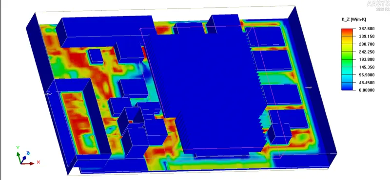
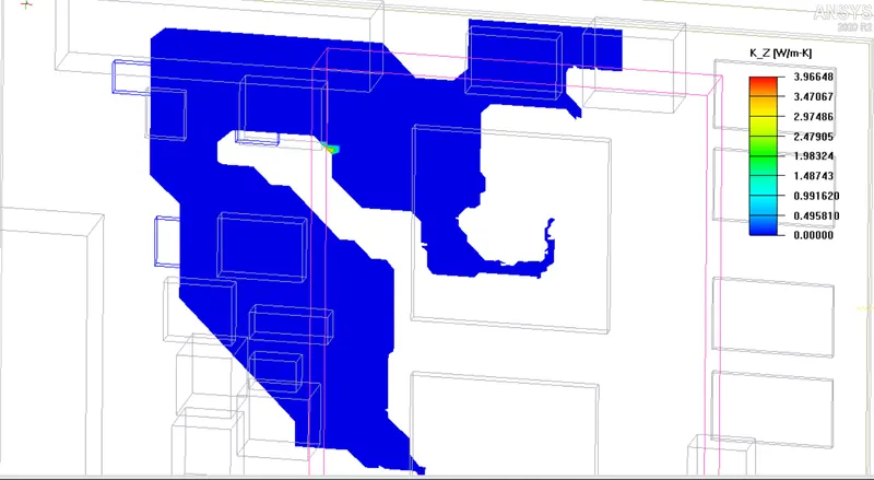
The thermal conductivity in z direction is maximum with area of heat distribution maximum, on the other side thermal conductivity in x and y axis is very minimum with few hot spot areas.
Force convection model:
Meshing & BC setting:
put the actual components back into the model
Highlight the two wall objects created for the “conduction only" model and drag them into the Inactive folder. Click on the Cabinet and Autoscale it from the Edit window.
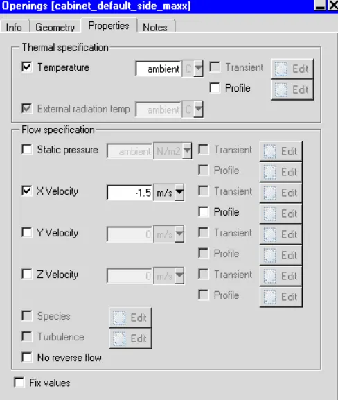
assign an X Velocity of -1.5 m/s for Max x side of the cabinet
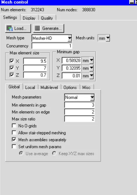
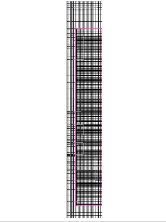
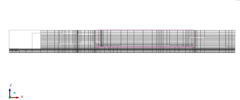
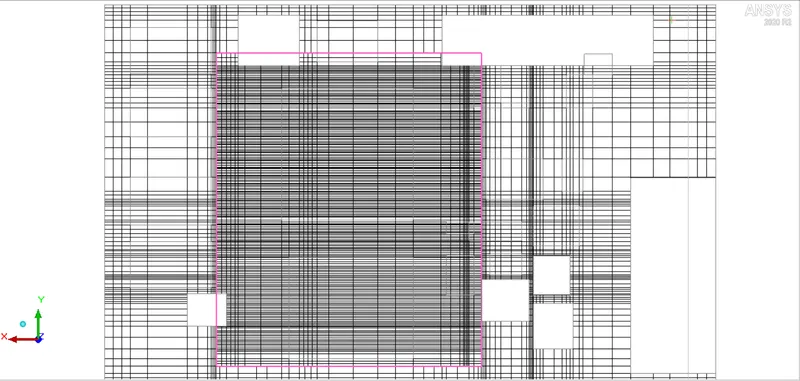
Generate mesh. Specify a Max element size for X, Y, Z as 9.5, 7, and 0.7 mm respectively.
PCB model for all components
Importing the board layer thickness and via layer information:
Metal fraction:
Trace by single color
Trace by layer
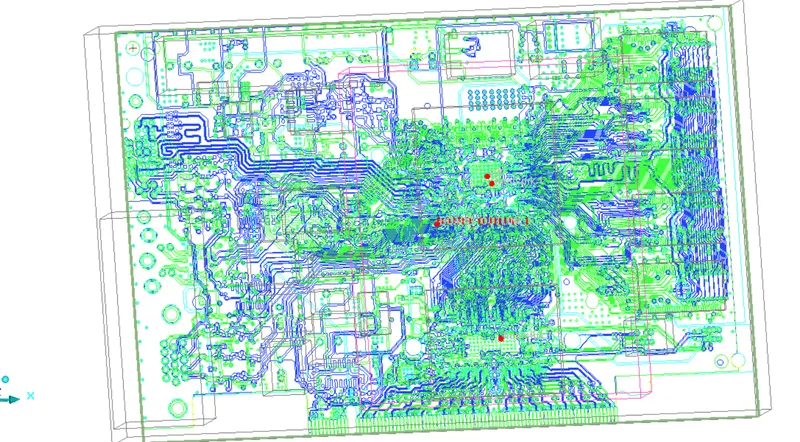
Trace by colour
Mesh settings:
Mesh x
Mesh y
Mesh z
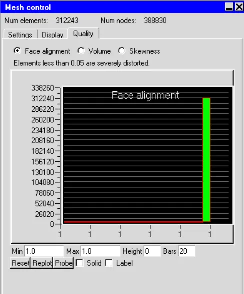
Face alignment
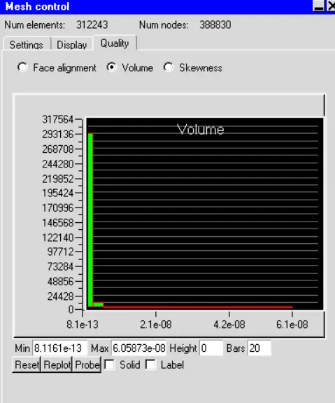
Volume
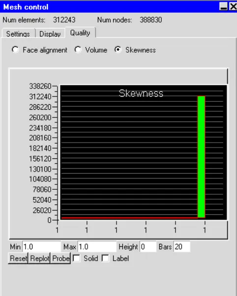
Skewness
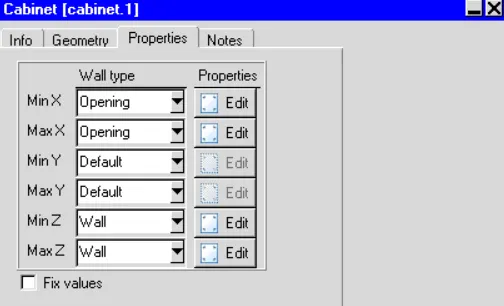
Cabinet inlet wall BC
Cabinet outlet wall BC
Boundary condition:
Flow BC
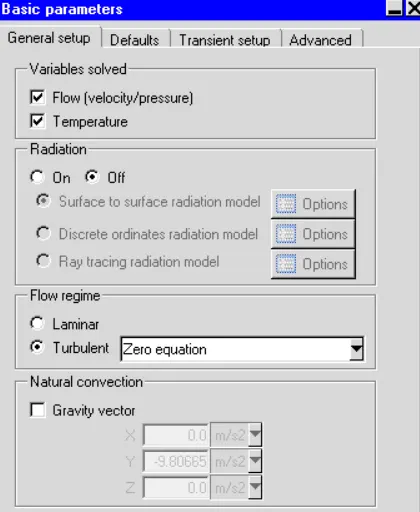
Inlet velocity BC
Convergence parameter
Advanced settings:
Post processing:
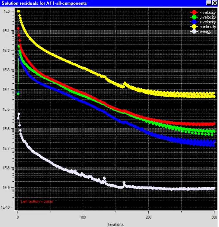
Iteration
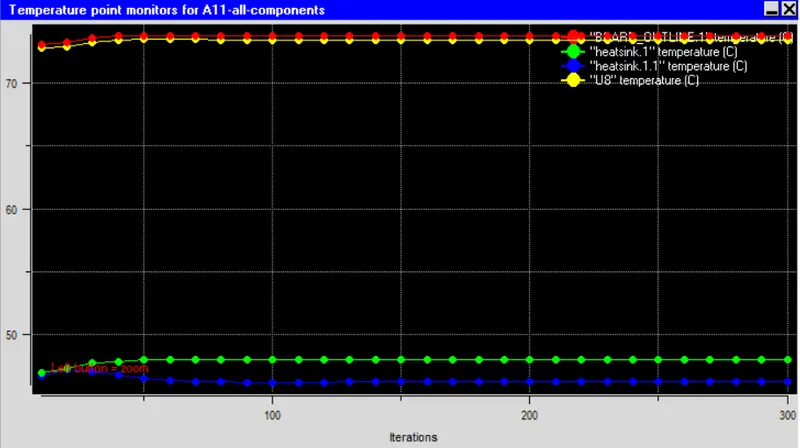
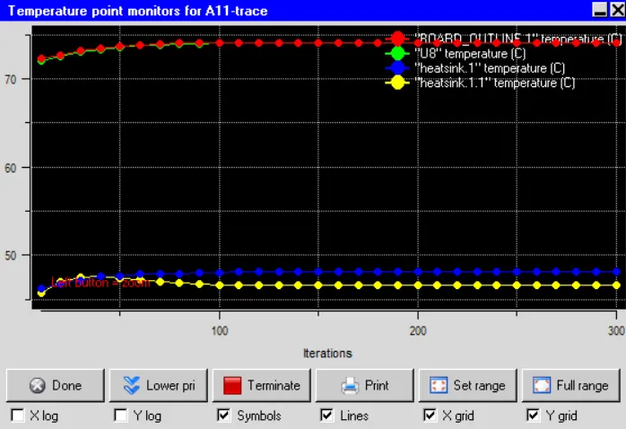
Monitor points
Board Temperature contour
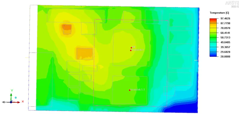
The board temperature distribution with all components shows maximum of 97.64 degree C and minimum of 20 degree C. At the cabinet outlet the temperature is minimum and maximum at the heat generated sources.
Temperature contour
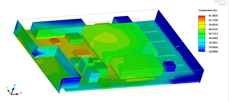
At the system level , the max temp is found at the heat generating source, which is at temperture 97 degree c, while at the outlet of the cabinet the temperature is 20 degree C.
The heat sink dissipates the maximum heat where the temperature is at 49 degree.
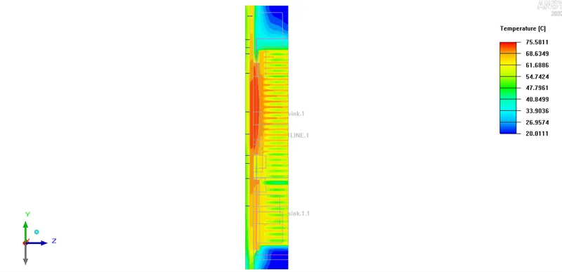
Temp x
Temp y
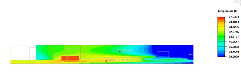
Temp z
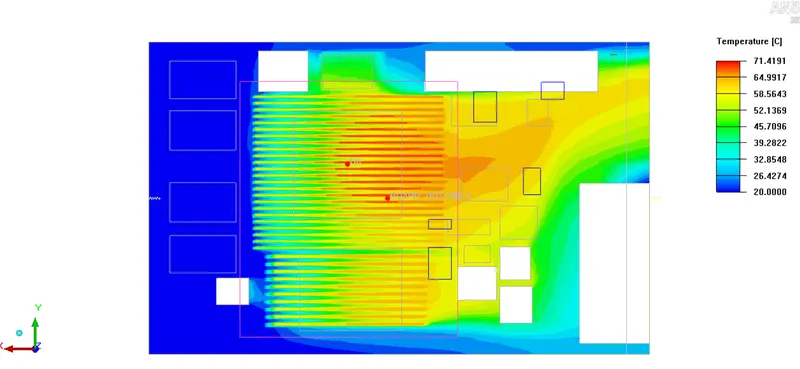
The temperature at the junction is maximum, while at the outlet is minimum. The heat sink temperature is 52 degreeC, the forced cooling is optimally from inlet to outlet.
Conductivity in x direction
Conductivity in y direction
Conductivity in z direction
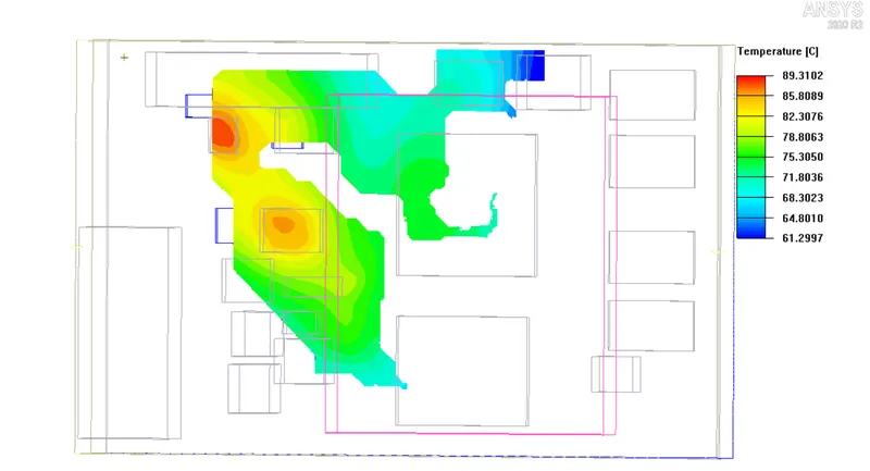
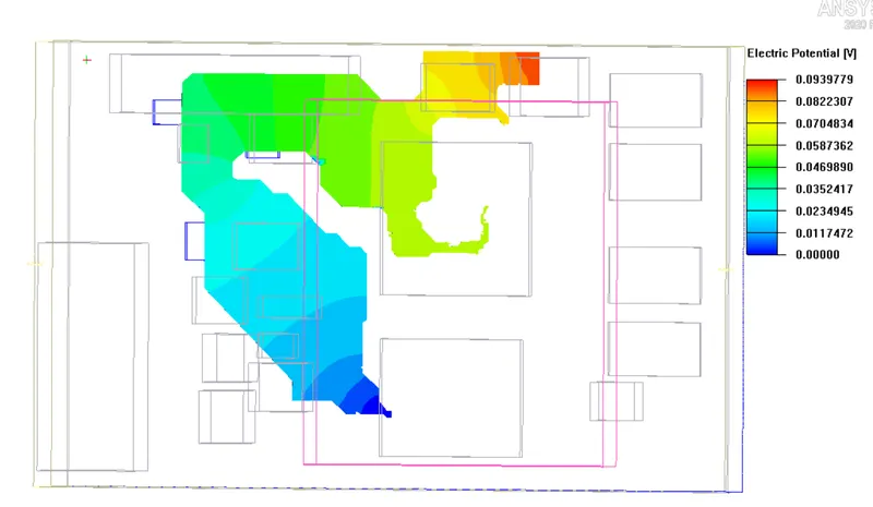
Joule/Trace Heating
Since PCB traces have electrical resistance, they heat up as current flows through them.Modeling this phenomenon will provide us with an accurate prediction of the temperaturedistribution in the PCB, which can be important, for example, in evaluating the performance ofthe cooling system. The model in the tutorial contains imported traces and will be used in thistutorial. You will determine the Joule/trace heating capacity of the traces.
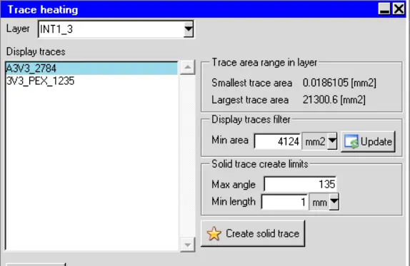
- Build the Model – Edit the Board outline of the previous model to open the model trace heating
panel select INT1_3 layer -> filter the trace to view by setting Min Area in the Display traces
filter group box use a Min Area of 4124 mm2
b.Before you create a solid trace of trace A3V3_2261 set the Max angle filter to 135 and the Min
length filter to 1.0 m to ignore the fine details in the trace geometry and reduce the mesh count.
c. Create a solid polygonal solid block for trace A3V3_2261
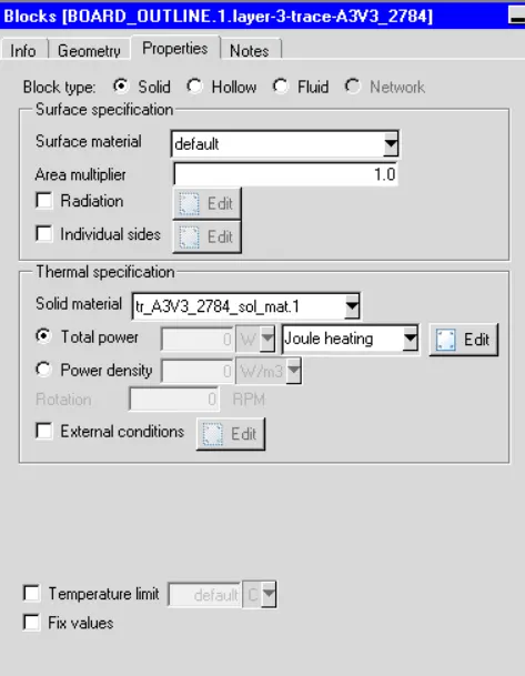
d. Select the polygonal trace just created from the Model manager window à Under Thermal
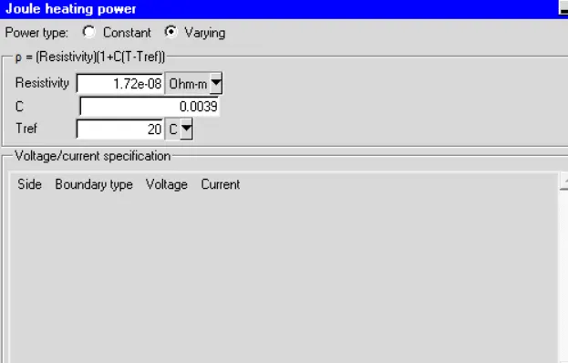
specification next to Joule heating, click Edit to open the Joule heating power panel. à Set
Resistivity, temperature coefficient (C), and reference temperature (Tref)
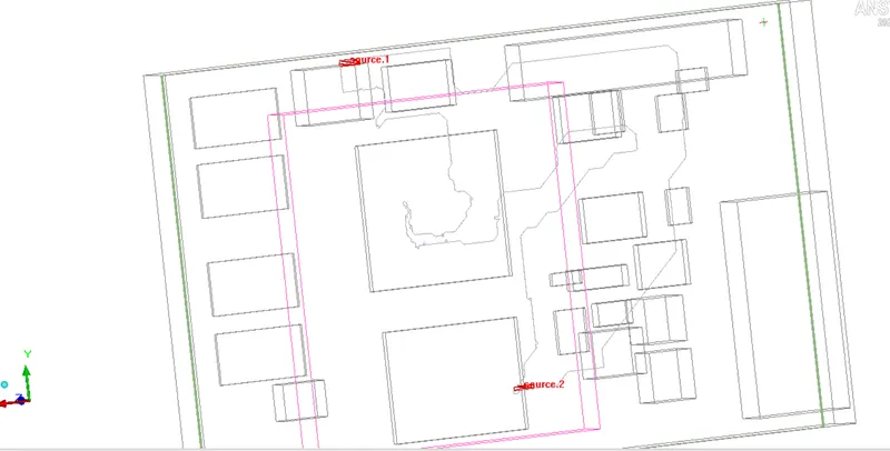
e. One source is for the current source (source.1) and the other for the voltage source (source.2).
Both sources are created at the same layer as the layer of the wire in. The area of each
source is the area to apply the voltage or the current. • The recommendation of the source
objects pair for joule heating is the current-voltage pair or voltage- voltage pair.
PCB trace model
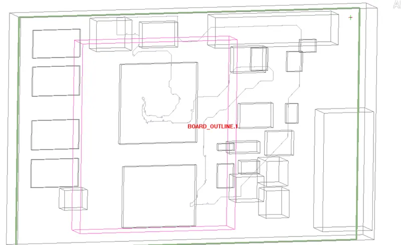
PCB model with source
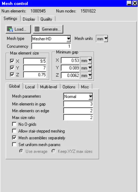
Mesh settings:
Mesh x
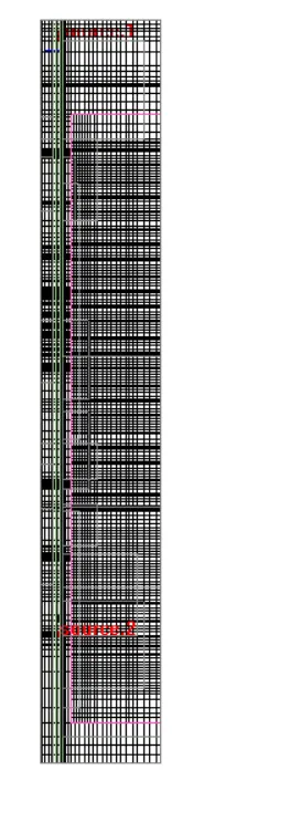
Mesh y
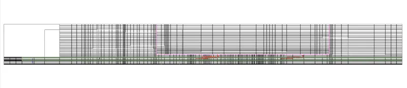
Mesh z
Boundary condition:
Trace BC
Trace properties
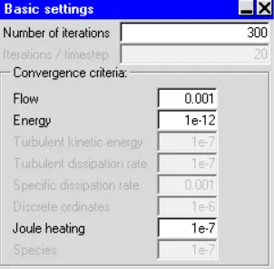
Basic parameter
Joule BC
Joule trace BC
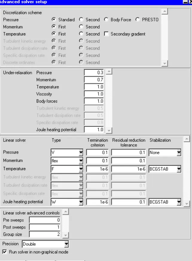
Advanced settings:
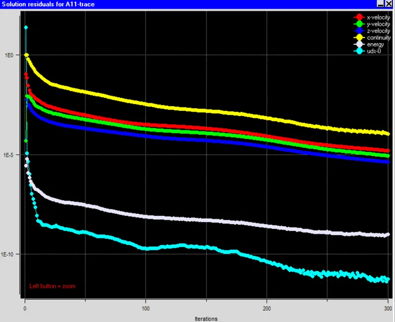
Post processing:
Iteration
Monitor points
Temperature contour
Electrical potential
Conductivity in x direction
Conductivity in y direction
Conductivity in z direction
Conclusions:
- The board level simulation is performed to check the thermal distribution. The trace layer shows the different metal fraction across different layers.
- At the system level simulation, the temperature cooling is maximised and the trace layer is identified. The temperature distribution shows maximum heat dissipation due to forced convection.
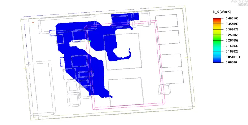
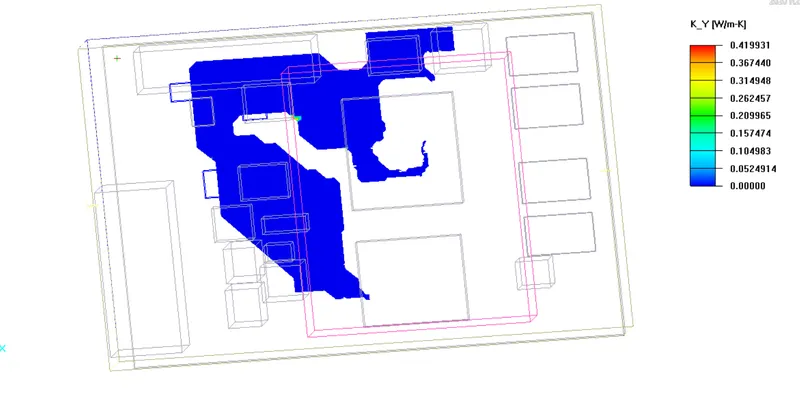
- The joule tracing is done to identify the heat zones and the electric potential at the board level. Also the thermal conductivity shows maximum at the z axis and minimum at the other axis.