Embedded Systems Architecture: Block Diagram, Layers and Worked Examples
How an embedded system's processor, memory, peripherals and software layers fit together, with checked numbers: von Neumann vs Harvard bus cycles, the Cortex-M4 memory map and a bit-band address, interrupt latency in nanoseconds, and a rate-monotonic RTOS deadline check.
Key takeaways
- Embedded systems architecture is how a device's hardware (processor, memory, peripherals, buses) and software (drivers, an optional RTOS, middleware, application) are arranged so that one job runs reliably, on time and within a fixed memory and power budget.
- Von Neumann puts code and data on one bus; Harvard gives them separate buses. In Arm's own datasheets the Cortex-M0+ is von Neumann and the Cortex-M3 and M4 are Harvard (checked 17 Nov 2026).
- In our idealised word-copy example, a single bus needs 6 cycles per loop iteration and a Harvard core needs 4, which is 1.5 times the throughput.
- A Cortex-M4 starts running an interrupt handler 12 clock cycles after the request (Arm, zero-wait-state memory). At 168 MHz on an STM32F407 that is 71.4 ns.
- Three periodic tasks using 70% of the CPU pass the rate-monotonic test (the bound is 78% for three tasks). Response-time analysis shows the slowest task finishing at 4.75 ms against a 10 ms deadline.
Embedded systems architecture is the plan of how a device's processor, memory, peripherals and software layers are arranged and connected to do one dedicated job. It decides where code and data live, how the CPU reaches them (one bus or two), how fast the system reacts to an interrupt, and how tasks share the processor so that every deadline is met.
This guide walks through the hardware block diagram and the software layers, then von Neumann vs Harvard and the memory map. After that come interrupts and the three common ways to structure firmware: super loop, interrupt-driven and RTOS. Every calculation is worked through with real chip numbers from Arm and ST datasheets, and the script that checks them is kept with the article. It is written for engineering students and freshers in India preparing for embedded roles and interviews.
What is embedded systems architecture?
Embedded systems architecture is the structure of a dedicated computer inside a product: which processor it uses, how its memories and peripherals are connected, and how its software is layered on top. A good architecture meets the product's timing, memory, power, cost and safety limits with margin, and keeps the code maintainable as features are added.
A laptop is built to run any program you install. An embedded system is built around one job: an electric scooter's motor controller, a washing machine's control board, a car's airbag unit, an electricity meter. Because the job is known in advance, the architect can size everything for it: just enough RAM, a processor that is fast enough for the worst case, and a software structure that guarantees the most urgent work always runs first. If you are new to the idea, start with our explainer on what an embedded system is; this article goes one level deeper, into how such a system is put together.
Architects look at it from two sides. Hardware architecture covers the processor core, memories, buses and peripherals. Software architecture covers the layers of code and how work is scheduled. The two have to be designed together. Whether you need an RTOS, for example, depends on how many timing-critical jobs the hardware must handle.
What are the main hardware components of an embedded system?
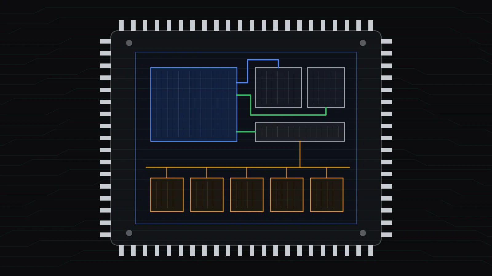
The main hardware components are the processor core, which runs the code; non-volatile flash, which holds the program; SRAM for variables and the stack; peripherals such as GPIO, timers, ADCs and communication controllers; a bus matrix that connects them; and clock, reset and power circuits. In a microcontroller all of these sit on one chip.
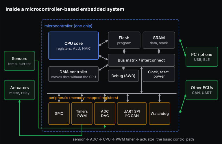
| Block | What it does | Example: STM32F407 |
|---|---|---|
| Processor core | Fetches and executes instructions; the NVIC (nested vectored interrupt controller) decides which interrupt runs first | Arm Cortex-M4 with FPU, up to 168 MHz |
| Flash | Non-volatile program and constant storage | Up to 1 MB |
| SRAM | Variables, stack, heap; lost at power-off | 192 KB (includes 64 KB core-coupled memory) |
| Peripherals | Talk to the outside world: GPIO, timers and PWM, ADC, UART, SPI, I²C, CAN, USB | Each controlled through memory-mapped registers |
| DMA controller | Copies data between peripherals and memory without the CPU | Moves ADC samples into a buffer while the CPU computes |
| Bus matrix | Lets several masters (CPU, DMA) reach memories and peripherals at the same time | AHB/APB buses |
| Clock, reset, power, watchdog | Keep the chip running at the right speed and restart it if the software hangs | Watchdog resets a stuck program |
A microprocessor-based system (an MPU running Linux, for example) moves the memory off-chip and adds a memory management unit, caches and an operating system. The architecture questions stay the same; only the scale changes. The comparison table further down shows where each kind of chip fits.
What are the layers of embedded software?
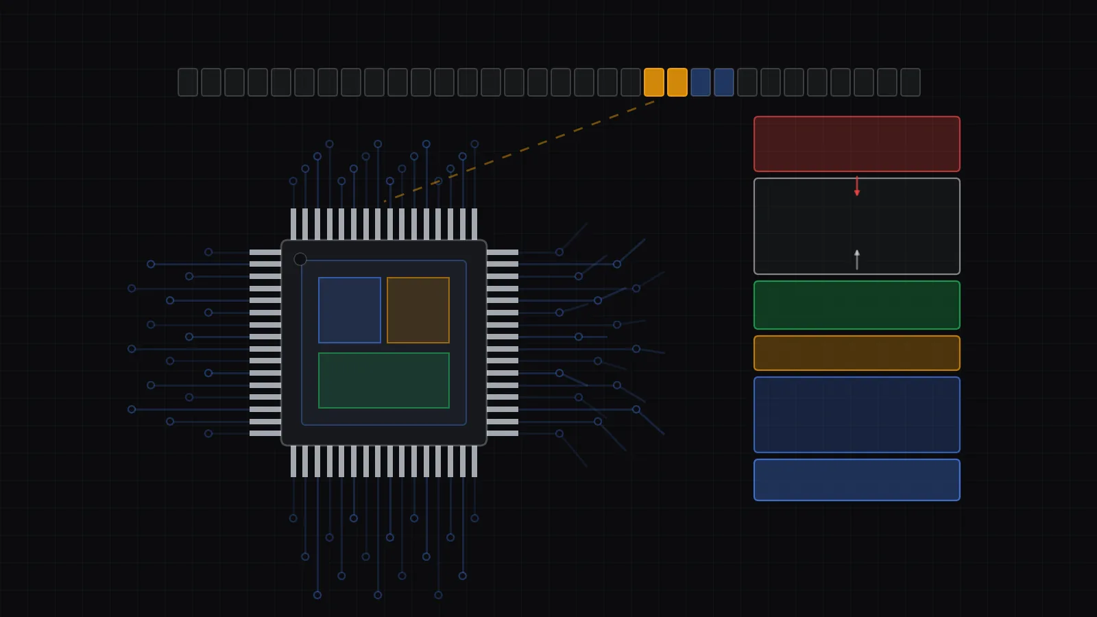
Embedded software is usually built in layers. Startup code and a hardware abstraction layer (HAL) or board support package (BSP) sit at the bottom, device drivers above them, then an optional real-time operating system (RTOS) kernel, then middleware such as protocol stacks and file systems, and the application on top. Each layer calls only the one below through a fixed interface.
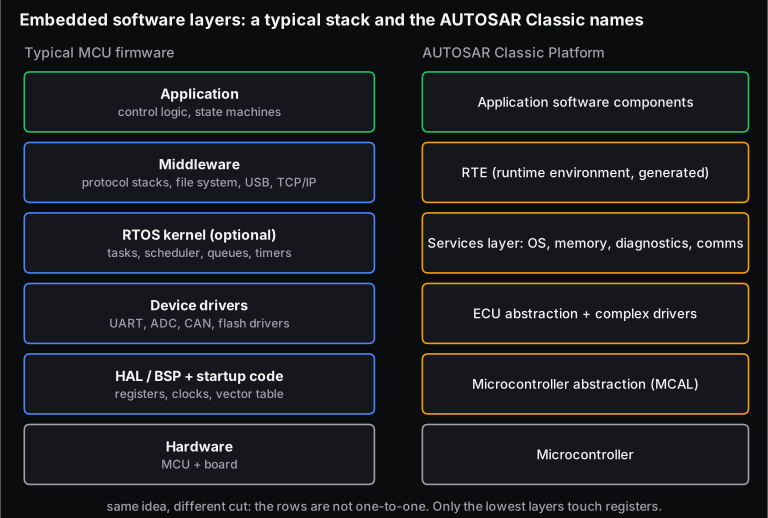
- Startup code and HAL/BSP. Startup code sets up the stack, the vector table and the clocks, then calls
main(). The HAL hides register details behind functions such as "set pin high" or "start ADC conversion", so higher layers do not change when the chip changes. - Device drivers. Code for each peripheral: a UART driver with transmit and receive buffers, a CAN driver, a flash driver. Drivers handle the interrupts their hardware raises.
- RTOS kernel (optional). Splits the work into tasks with priorities and provides queues, semaphores and timers. FreeRTOS, a widely used open-source example, is MIT-licensed; its current kernel line is V11 (V11.3.3 was the latest release on GitHub when we checked on 17 Nov 2026).
- Middleware. Reusable stacks that sit on drivers: TCP/IP, USB, Bluetooth, a FAT file system, CAN diagnostics.
- Application. The product logic: a motor control loop, a battery state-of-charge estimate, a user-interface state machine.
Automotive ECUs formalise this in AUTOSAR. The Classic Platform defines three software layers on the microcontroller: the application, the runtime environment (RTE) and the basic software. The basic software is split into services, ECU abstraction and microcontroller abstraction (MCAL). The RTE and basic software are generated from configuration files, not written by hand, so application components can move between ECUs with little change. Skill-Lync's Introduction to Automotive Embedded Systems and AUTOSAR course covers this stack in detail.
What is the difference between von Neumann and Harvard architecture?
In von Neumann architecture, instructions and data share one memory and one bus, so the CPU fetches an instruction or accesses data, but not both in the same cycle. Harvard architecture uses separate buses (and often separate memories) for instructions and data, so it can fetch the next instruction while the current one reads or writes data.
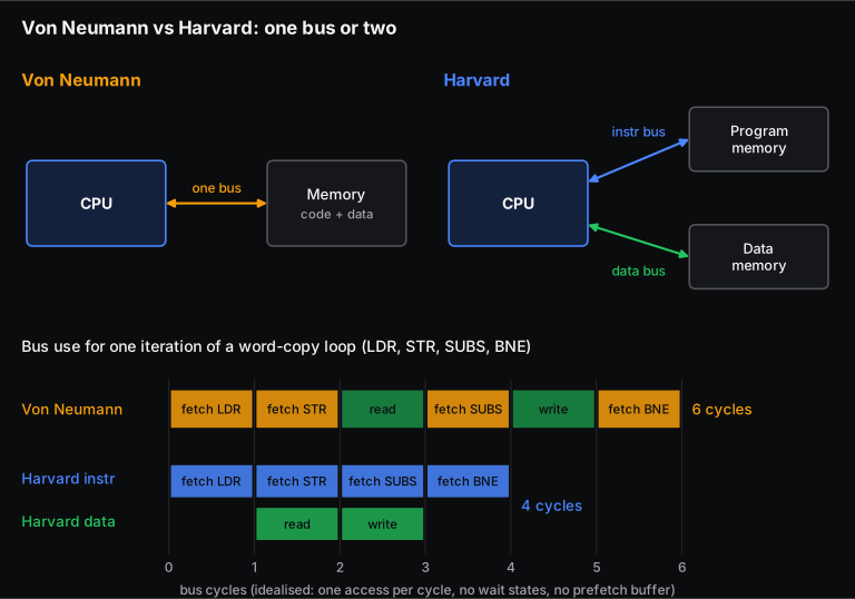
Worked example: how much faster is the Harvard bus?
Take the inner loop of a word copy on an Arm core: LDR (load a word), STR (store it), SUBS (decrement the counter), BNE (branch back). Each iteration has 4 instruction fetches and 2 data accesses. Assume one bus access per clock cycle, no wait states and no prefetch buffer:
That is 6 bus cycles per iteration on the shared bus and 4 on the Harvard core.
Copying 1,000 words therefore takes 6,000 vs 4,000 bus cycles, which at 168 MHz is 35.7 µs vs 23.8 µs. That is 1.5 times the throughput, from the bus structure alone.
Real chips blur this neat result, and the limits matter. Thumb instructions are mostly 16 bits wide and are fetched 32 bits at a time, so one fetch can bring in two instructions. Prefetch buffers, caches and flash accelerators hide fetch time, and flash wait states add it back. Treat the 1.5 times as an illustration of why the separate bus helps, not a benchmark. To compare chips, measure with a cycle counter on your own code.
Which real microcontrollers use which?
| Von Neumann | Harvard | |
|---|---|---|
| Buses | One shared bus for instructions and data | Separate instruction and data buses |
| Instruction fetch during a data access | No: they take turns | Yes: they overlap |
| Hardware cost | Lower: fewer bus lines, simpler interconnect | Higher: more bus lines and interfaces |
| Flexibility | Code and data can share any memory | Pure Harvard keeps them apart; most modern MCUs relax this |
| Examples (vendor documents) | Arm Cortex-M0+ (single AHB-Lite bus, 2-stage pipeline); RP2040's two cores are M0+ | Arm Cortex-M3 (ICode, DCode and system buses), Cortex-M4 (3-stage pipeline Harvard); Microchip AVR (separate program and data memories and buses) |
The old idea that Harvard is "slower and uses more power" is wrong. Its advantage is exactly that it can do two transfers at once. Its cost is extra hardware.
Most Cortex-M chips are, strictly, a mix of the two. The core has separate instruction and data bus interfaces, but both reach one shared 4 GB address map. So code can run from SRAM and constant tables can be read from flash. Textbooks often call this a modified Harvard architecture.
What is a memory map, and why does it matter?
A memory map is the table of which address ranges belong to which memory or hardware block. On a Cortex-M4 it is fixed by Arm: a 4 GB address space with code from 0x00000000, SRAM from 0x20000000, peripherals from 0x40000000, and the core's own private peripherals, such as the interrupt controller, from 0xE0000000. Firmware controls hardware by reading and writing these addresses.
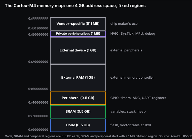
"Memory-mapped I/O" is the reason a single line of C can switch on an LED. A peripheral's control register is just an address in the peripheral region. Writing a value to it changes the hardware. This is also why the linker script matters: it tells the toolchain where flash and SRAM sit on your exact chip, where the vector table goes (address 0x00000000, where the core reads its initial stack pointer and reset vector), and how much room the stack has.
Worked example: a bit-band address
The Cortex-M3 and M4 can optionally map each bit of the first 1 MB of SRAM to its own 32-bit "alias" word, so that one write sets or clears a single bit atomically, with no read-modify-write that an interrupt could break. Arm gives the formula:
Here is the alias address, the start of the alias region, the byte offset into the bit-band region and the bit number (0-7).
Say a status flag is bit 5 of the byte at 0x20000301. The SRAM bit-band region starts at 0x20000000 and its alias region at 0x22000000. The byte offset is 0x301, which is 769, so:
Writing 1 to address 0x22006034 sets that one bit. Our script reproduces Arm's own published examples first (for instance 0x200FFFFF bit 0 maps to 0x23FFFFE0) before computing this one. Arm lists bit-banding as optional and not every Cortex-M chip has it, so check your chip's reference manual before relying on it.
How do interrupts fit into embedded architecture?
An interrupt is a hardware signal that makes the processor pause its current work, save its state and run a short handler, called an interrupt service routine (ISR), then resume. Interrupts let an embedded system react to events within microseconds without constantly checking for them. The interrupt controller (the NVIC on Arm Cortex-M) decides which pending interrupt runs first, by priority.
Interrupt latency is the time from the request to the first instruction of the handler. Arm publishes it in clock cycles for zero-wait-state memory:
| Core | Latency (cycles) | Example clock | Latency in time |
|---|---|---|---|
| Cortex-M4 | 12 | 168 MHz (STM32F407) | 71.4 ns |
| Cortex-M0+ | 15 | 133 MHz (RP2040) | 112.8 ns |
| Cortex-M0+ | 15 | 48 MHz | 312.5 ns |
| Cortex-M0 | 16 | 48 MHz | 333.3 ns |
The arithmetic is cycles divided by clock frequency, for example . These are best cases. Flash wait states, a higher-priority interrupt already running, or a code section that disables interrupts all add to them. In a real design you budget the worst case, not the datasheet figure. The practical rules follow from this: keep ISRs short, set a flag or push data into a queue, and do the heavy processing in the main loop or a task.
Super loop, interrupt-driven or RTOS: which software architecture should you use?
Use a super loop for simple devices with one or two jobs and relaxed timing. Use interrupt-driven foreground/background code when a few events need fast responses. Use an RTOS when you have several independent jobs with different deadlines, because its priority-based scheduler lets you prove that every deadline is met as features grow.
| Architecture and best use | Watch out for |
|---|---|
Super loop (bare metal): while(1) calls each job in turn. Best for simple sensors, toys and small controllers. | Response time is the whole loop; one slow job delays everything |
| Foreground/background: ISRs handle urgent events, the loop does the rest. Best for most small products that must react fast to a few events. | Data shared between ISR and loop needs care (volatile, critical sections) |
| RTOS: prioritised tasks; the scheduler always runs the highest-priority ready task. Best for motor control with communication, BMS, connected devices and automotive ECUs. | RAM for each task's stack, priority inversion, more to learn and test |
| Embedded Linux: a full OS with processes, drivers and file systems on an MPU. Best for gateways, infotainment, cameras and HMIs. | Not hard real-time by default; boot time; far more memory |
How do you check that an RTOS will meet its deadlines?
For periodic tasks with rate-monotonic priorities (shorter period gets higher priority), first add up CPU utilisation. If it is below Liu and Layland's bound, , which is 0.78 for three tasks, every deadline is guaranteed. If it is above the bound, run response-time analysis, which gives each task's exact worst-case finishing time.
Here is a motor controller with three tasks. Each has a worst-case execution time and a period , and its deadline equals its period:
| Task | C (ms) | T (ms) | C/T |
|---|---|---|---|
| Current control loop | 0.25 | 1 | 0.25 |
| Speed control loop | 1.0 | 5 | 0.20 |
| CAN messages + diagnostics | 2.5 | 10 | 0.25 |
Step 1: utilisation test.
Because 0.70 is at most 0.7798, the set is schedulable. As grows, the bound falls towards . The test is sufficient but not necessary: a set that fails it may still be fine, which is what Step 2 checks.
Step 2: response-time analysis. A task's worst-case response time is its own execution time plus every pre-emption by higher-priority tasks:
Solve it by repeating until stops changing. For the diagnostics task, start from . In each line, the first multiplier is (current-loop runs) and the second is (speed-loop runs), both using the previous value of :
It converges at 4.75 ms, well inside the 10 ms deadline. The speed loop works out to 1.5 ms (deadline 5 ms) and the current loop to 0.25 ms.
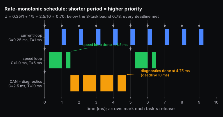
Now suppose a new diagnostic feature takes the third task to 4 ms. Utilisation becomes 0.85, above the 0.78 bound, so the quick test can no longer promise anything. Response-time analysis still gives 8.0 ms, inside the 10 ms deadline, so the design still works, but with only 2 ms of margin. This is the kind of check that tells an architect whether a feature fits on the current chip or needs a faster one.
A word of honesty about these numbers: the analysis is only as good as , the worst-case execution time. It assumes independent tasks and ignores RTOS overhead, interrupts and blocking on shared resources. On real projects you measure on the target, add those terms, and keep margin.
MCU, MPU or SoC: which processor architecture fits which product?
Choose a microcontroller (MCU) when the job is real-time control with modest memory. Choose a microprocessor (MPU) or system-on-chip running Linux when you need a display, networking, file systems or heavy computation, and can accept less deterministic timing. Many products use both: an MPU for the user interface and an MCU for the hard real-time control.
| Chip (example) | Core and memory | Software and products |
|---|---|---|
| STM32F407 (MCU) | 1 × Cortex-M4F, up to 168 MHz, Harvard; up to 1 MB flash, 192 KB SRAM on chip | Bare metal or RTOS; motor drives, BMS, industrial controllers |
| RP2040 (MCU) | 2 × Cortex-M0+, up to 133 MHz, von Neumann; 264 KB SRAM on chip, external QSPI flash | Bare metal, RTOS, MicroPython; low-cost controllers, teaching boards |
| BCM2712 in Raspberry Pi 5 (MPU/SoC) | 4 × 64-bit Cortex-A76 at 2.4 GHz; external SDRAM, caches | Linux; gateways, vision, HMIs, prototyping |
For more on how processor families differ, see types of processors in embedded systems.
How do you choose an architecture for a new embedded project?
Start from the requirements, not the chip. List every job with its deadline, the fastest event you must catch, the memory each feature needs, power and cost limits, and any safety standard. Then pick the simplest processor and software structure that meets the worst case with margin, and check it with numbers before building.
- List the jobs and their timing. For each: period or trigger, deadline, worst-case execution time. This is the task table above.
- Find the tightest latency. If a fault must shut off a motor within, say, 2 µs, that rules out software polling and points to interrupts, or to a hardware comparator that trips the PWM directly.
- Budget memory. Add code size, buffers, one stack per RTOS task and the middleware's needs, then keep 30-50% headroom for features added later. That margin is a common engineering habit, not a standard.
- Pick the software structure using the super loop / interrupt / RTOS / Linux table.
- Check safety and certification. Automotive work follows ISO 26262 functional safety, which affects tool choice, coding rules and whether you need features such as a memory protection unit.
- Prototype and measure. Use a development board, a cycle counter and a logic analyser to measure real execution times and latencies, and re-run the schedulability check with measured numbers.
Where is embedded architecture knowledge used in Indian jobs?
Architecture questions come up in almost every embedded interview in India. Interviewers ask about von Neumann vs Harvard, ISR rules, volatile, memory maps, stack overflow, RTOS scheduling and priority inversion. Our embedded C interview questions with tested code cover the coding side.
Based on 3,711 Skill-Lync placement records up to 7 Nov 2026 (data snapshot of 15 Nov 2026), learners placed in embedded roles had a median offer of ₹4.0 LPA. The middle half of offers fell between ₹3.5 and 5.0 LPA (n = 278). Cyient (18) and Nexteer Automotive (17) hired the most. Read these as a starting point, not a market average. They are a self-selected sample of Skill-Lync learners, mostly early-career offers from 2022 and 2023 (n = 133 and 98; only 42 from 2024). We will update them as new placements come in. For role-level detail, see embedded engineer salaries and what an embedded developer does day to day.
How can you learn embedded systems architecture hands-on?
The fastest way to make this stick is to build on a real or simulated board. Blink an LED through a register write, measure an interrupt's latency with a GPIO toggle and an oscilloscope, then move the same job into FreeRTOS tasks and watch the schedule. For reading, our free Microcontrollers book has units on ARM processors and on RTOS and IoT.
Skill-Lync's Fundamentals of Embedded Systems (12 weeks) covers ARM and AVR architecture, GPIO, ADC, timers, interrupts and serial protocols. The Pre-Graduate Program in Embedded Systems adds bare-metal programming, testing and projects for freshers. You can compare all options on our embedded systems courses page. If you are not sure which fits your branch and year, book a free call with a Skill-Lync counsellor.
Frequently asked questions
What are the two types of embedded system architecture?
The two classic types are von Neumann, where instructions and data share one memory and one bus, and Harvard, where they have separate buses so an instruction fetch and a data access can happen in the same cycle. Many modern microcontrollers, including Arm Cortex-M3 and M4, use a modified Harvard design with one shared address map.
Is ARM Cortex-M von Neumann or Harvard?
It depends on the core. Arm's datasheets list the Cortex-M0+ as von Neumann, with a single AHB-Lite bus. The Cortex-M3 has three AHB-Lite interfaces (ICode, DCode and system) in a Harvard bus architecture, and Arm describes the Cortex-M4 as a 3-stage pipeline Harvard design. All of them share one 4 GB memory map.
Why do many microcontrollers use Harvard architecture?
Because a separate instruction bus lets the core fetch the next instruction while the current one reads or writes data, which raises throughput at the same clock speed. In our idealised copy-loop example that is 4 cycles per iteration instead of 6. The cost is extra bus hardware, which is small on modern chips.
What is the role of an RTOS in embedded systems architecture?
An RTOS splits firmware into prioritised tasks and always runs the most urgent ready task, preempting less urgent ones. That makes timing predictable and analysable: with rate-monotonic priorities you can prove deadlines are met, as in the three-task example where the slowest task finished at 4.75 ms against 10 ms. It also provides queues, semaphores and timers.
What is the difference between a microprocessor and a microcontroller in embedded design?
A microcontroller puts the CPU, flash, SRAM and peripherals on one chip and suits real-time control, like the STM32F407 with 1 MB flash and 192 KB SRAM. A microprocessor needs external RAM and storage, usually runs Linux, and suits displays, networking and heavy computation, like the quad-core Cortex-A76 in a Raspberry Pi 5.
Is embedded systems architecture asked in interviews for freshers?
Yes. Freshers in India are routinely asked to explain von Neumann vs Harvard, what happens when an interrupt fires, why ISRs must be short, what volatile does, how memory is laid out (flash, SRAM, stack, heap) and how an RTOS scheduler decides which task runs. Working one numerical example, like interrupt latency, makes answers stand out.
Sources and further reading
- Arm, Cortex-M4 Devices Generic User Guide (DUI 0553B): 3-stage pipeline Harvard architecture, memory map, bit-banding formula. Accessed 17 Nov 2026.
- Arm, Cortex-M0+ Processor Datasheet: AHB-Lite, von Neumann bus architecture, 2-stage pipeline. Accessed 17 Nov 2026.
- Arm, Cortex-M3 Datasheet: 3 AHB-Lite interfaces (ICode, DCode, system), Harvard bus architecture. Accessed 17 Nov 2026.
- Joseph Yiu, Arm Community, "A Beginner's Guide on Interrupt Latency" (2016): 16 / 15 / 12 / 12 cycles for M0 / M0+ / M3 / M4.
- STMicroelectronics, STM32F407/417 product line: Cortex-M4 with FPU at 168 MHz, up to 1 MB flash, 192 KB SRAM.
- Raspberry Pi, RP2040 datasheet: dual Cortex-M0+ up to 133 MHz, 264 KB SRAM.
- Raspberry Pi, "Introducing Raspberry Pi 5" (2023): BCM2712, quad-core Cortex-A76 at 2.4 GHz.
- Microchip, AVR42787 AVR Software User Guide: AVR is Harvard, with separate memories and buses for program and data.
- C. L. Liu and J. W. Layland, "Scheduling Algorithms for Multiprogramming in a Hard-Real-Time Environment", Journal of the ACM 20(1), 1973: rate-monotonic utilisation bound.
- FreeRTOS-Kernel releases on GitHub and licence: V11.3.3 latest, MIT licence. Accessed 17 Nov 2026.
- ISO 26262-1:2018, Road vehicles: Functional safety: the functional-safety standard for road-vehicle E/E systems.
- AUTOSAR, Classic Platform: application, RTE and basic software layers; services, ECU abstraction, microcontroller abstraction.
- Skill-Lync placement records, snapshot of 15 Nov 2026 (records up to 7 Nov 2026): embedded-domain offers, n = 278.