Project 1 - 40-V to 80-V adjustable output voltage boost reference design for LIDAR applications
To design a non-synchronous boost controller:
The NCV8871 is an adjustable output non−synchronous boost controller which drives an external N−channel MOSFET. The device uses peak current mode control with internal slope compensation. The IC incorporates an internal regulator that supplies charge to the gate driver. Protection features include internally−set soft−start, undervoltage lockout, cycle−by−cycle current limiting, hiccup−mode short−circuit protection and thermal shutdown. Additional features include low quiescent current sleep mode and externally−synchronizable switching frequency.
an adjustable output of between 40 V and 80 V capable of delivering a maximum of 100 mA of current to the load. This is an automotive design intended to power various applications such as LiDAR systems, which require an adjustable voltage supply.
Required Equipment:
Power supply
Load Resistors
DMMS
Oscilloscope
Auxillary Power Supply (for providing DC signal that controls the output voltage)
Vin = 6-27 VDC
Vout = 40VDC to 80VDC (adjustable)
Iout = 0.1A maximum
Fsw = 400KHZ Nominal
Using electronic loads may exhibit undersriable behavior due to the interaction of the regulation loop of the electronic load with the low output capacitance of the boost converter. it is recommended to use resistor loads instead
1) how will you decide the layer stack up:
The rules and criteira for managing a good stackup
1.ground plane boards are better because they allow signal routing in a microstrip or stripline configuration. It also significatly reduces the ground impedance and therfore the ground noise
2. high speed signals should be "routed" on intermediate layers located between the various levels In this way ground planes can act as a shield and contain the radiation coming from the tracks at high speed
3. a signal layer must always be adjacent to a plane;
4. Multiple ground planes are very advantageous, since they lower the board's ground impedance and reduce radiation in a common way;
5. the power and mass planes must be rigorously coupled together;
To achieve all these objectives, it is necessary to operate with a minimum of eight layers. Moreover:
1. from a mechanical point of view, it is advisable to implement a cross section to avoid deformations;
2. configurations should be symmetric. For example, on an eight-layer PCB, if level 2 is a plane, level 7 should also be a plane;
3. if the signal levels are next to the levels of the plane (ground or power) the return current can flow on an adjacent plane reducing the inductance of the return path to a minimum;
4. to further improve noise and EMI performance, insulation between a signal layer and its adjacent plane can be made even thinner;
5. an important consideration to be done is the thickness of each signal layer. There are standard thicknesses together with the properties of different types of printed circuit material. When selecting the materials, it is advisable to consider their electrical, mechanical and thermal properties;
6. Use excellent software to help you design your stackup. All this should be done in order to choose the correct materials from the library and perform impedance calculations based on the materials and their dimensions.
2)How do you calculate the trace width, via size and trace length.
what is a pcb trace?
The role of a PCB is to conduct signals must travel on a path. PCB traces act as the transmission paths for these signals and data. They link various PCB components such as the IC, Capacitors, and resistors therfore withouttraces a PCB cannot function properly
The transmitted signals consist of electric current; thus, materials for making traces must be good conductors of electricity and reasonably stable. The common material for making PCB traces is copper foil, but there are other options to consider. For instance, you can use aluminum or gold.
PCB Trace Resistance
Almost everything on the Earth displays resistance and other parasitic properties. PCB trace resistance is an important factor that must be established and scrutinized during the design phase. While copper is the most suitable material for making traces, it displays diverse compositions and properties. The circuit board trace resistance can cause various design and implementation problems. As the PCB becomes more complex, the problems also increase.
How to Calculate the PCB Trace Resistance
Finding the circuit board trace resistance is as easy as applying the ohms principle in establishing a current voltage. Most design assemblies and working environments have incorporated trace calculators, facilitating the calculation of the PCB trace resistance. These calculators apply a standard formula to find the trace resistance as shown below:
R = (ρ * L / (T * W)) * (1 + α * (Tamb – 25 °C))
R stands for the resistance;
L is the trace length
T is the trace thickness
W is the trace width.
Tamb is the ambient temperature.
Besides, the equation has two constants – ρ and α, which represent the resistivity and resistivity temperature coefficient, in that order.
Analyzing the PCB Trace Resistance Equation
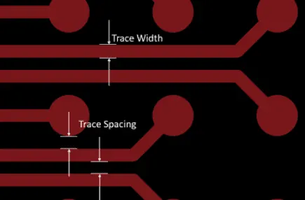
Trace Width
The trace width is basically the width of the copper foil, measured in mils – 0.0254 mm. Miscalculating the width might burn the trace. So, what defines the trace width? The trace width is determined by various factors like current, signal type, temperature, thickness, and others.
A PCB trace comprises width, thickness, and length. All these elements affect the functioning of the circuit board. Besides, it is normal to design PCBs with distinct widths based on their intended applications. For instance, traces designed for general applications, such as TTL demand smaller widths than those designed for power transmission. Though the best option seems to be selecting the biggest possible measurement, this is not always true.
Sometimes, circuit boards need to contain specific measurements; therefore, you can compromise on general principles to meet design requirements. This implies creating traces as wide as you would desire because of spacing.
How to Calculate the Trace Width
It is advisable to use a PCB trace width calculator to find the trace width. You simply need to enter the design specifications into the calculator, such as the tolerable current in amperage, the length of the copper foil, and the change in temperature caused by trail resistance. After entering these specifications, the device will carry out its computation and provide the least width you need to meet the design specifications you entered.
The computed width will facilitate the smooth transmission of current without damaging the board. The trace width of the inner layers may be bigger than that of the outer layers because they are more likely to generate more heat. The external layers produce less heat because of convection effects.
It is not advisable to just establish the general PCB trace or apply a simple principle to find the trace resistance. You should calculate both the circuit board traces and trace width. Doing so will assist you in minimizing the PCB trace resistance factor.
The PCB Trace Width Formula
The best way of finding the PCB trace width is by applying the trace width equation. The formula will enable you to find the tolerable current conducted through a particular trace. Below is the IPC 2221 trace width formula:
I=k*ΔT^0.44*A^0.725
I is the current, and it is always constant. ΔT is the temperature change, and A is the cross-sectional area. You can restructure the above equation to have the trace width on the left-hand side as shown below:
Area [mils^2] = (Current [Amps]/ (k*(Temp_Rise [deg. C]) ^ 0.44)) ^ (1/0.725)
However, to create the right width, you must consider your trace thickness.
Width [mils] = Area [mils^2]/ (Thickness [oz]*1.378[mils/oz])
You can only apply the above PCB trace width equation from amperes ranging from 0-35 because it allows temperature change from 100C to 1000C. Additionally, the formula accommodates a trace width of just 400 mils.
Disclaimer: Most circuit board service providers apply the PCB trace formula as the electronic industry standard and assume it to be right. Nevertheless, the formula may not be ideal for each design requirement. Thus, it is advisable to specify your trace width in the Gerber file and seek advice from the manufacturer on whether the specified width is ideal for your application.
Trace Thickness
As mentioned earlier, trace thickness is one of the main determinants of calculating trace width. You must consider the trace area if you want to keep your PCB components safe. The trace area narrows down to the trace thickness.
The trace thickness is a standard value, ranging from 0.008 to 0.24 inches. Therefore, your trace thickness should lie in between this range. Remember, it is the designer who selects the trace thickness, and just like the trace width, it varies from one trace to another on the same circuit board.
Additionally, it is essential to note that the size of the internal layer plays a significant role in determining the trace thickness. You can use half, one, or two ounces for your internal layers. To calculate the trace area, you can rely on the universal chart for accurate figures from the IPC 2152 standard. Another option is applying a trace width calculator supported by the IPC 2221 AND IPC 2152 standards.
Trace Length
As mentioned earlier, longer traces create a high resistance, implying that length is also an important PCB trace resistance consideration. You should aim to design a small board by minimizing the length of the traces. Though you will end up with short and wide traces, your PCB will have the quickest signal transmission time.
Trace Spacing
Trace spacing refers to the distance between two traces. Like the trace width and length, it is also an important trace resistance consideration. Importantly, trace spacing will enable you to prevent flashovers between two conductors. A flashover is a current breakdown that appears along the PCB surface or junction.
3) What is the drawback of having 2 layers PCB?
2 layer pcb is the most common type of PCB, and it is used in a wide variety of applications. If you are looking for a less expensive option, or if time is of the essence, 2-layer pcb may be the right choice for you. However, if you need more flexibility in terms of design, you may want to consider a different type of PCB, such as 4 layer PCB.