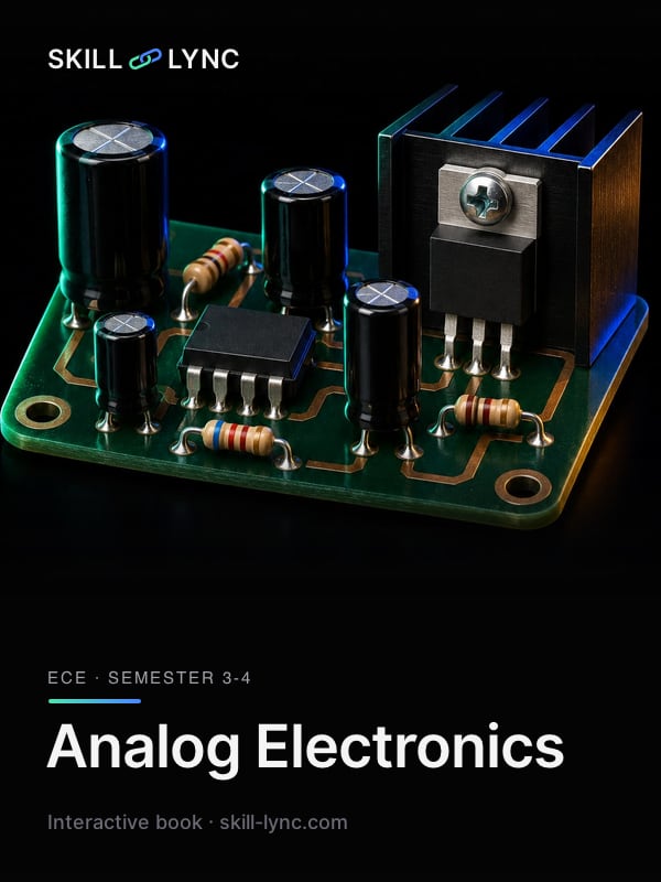
Analog Electronics
Drive a transistor amplifier until it clips, watch a Wien bridge oscillator start from noise, and step a SAR ADC through its binary search
25 chapters, 25 interactives, few words. Every chapter is mapped to the Anna University, VTU, SPPU, Mumbai University and KTU units it covers: the diode, rectifiers and regulators, wave shaping, transistor characteristics and biasing, CE, CC, CB and MOSFET amplifiers, low- and high-frequency response, cascode and differential amplifiers, current mirrors, negative feedback, oscillators, power amplifiers, the real op-amp and its linear and non-linear circuits, active filters, data converters, the 555 timer and the phase-locked loop. Logic gates and flip-flops are in the Digital Electronics book; thyristors and switching converters are in the Power Electronics book.
- AUEC3353, EC3451Electronic Devices and Circuits; Linear Integrated Circuits
- VTUBEC303Electronic Principles and Circuits
- SPPU204181Electronic Circuits
- MUECC302, ECC403Electronic Devices and Circuits; Linear Integrated Circuits
- KTUPCECT303Analog Circuits
By Skill-Lync · Updated 19 Nov 2026 · 25 chapters · 25 interactives · free, no sign-up
The PN junction diode: the diode equation, temperature and junction capacitance
Which syllabus covers thisAU EC3353 Unit IVTU BEC306A Module 2SPPU not in syllabusMU ECC302 Module 1KTU not in syllabus
What happens where P-type and N-type silicon meet?
Electrons from the N side and holes from the P side diffuse across the boundary and cancel each other, leaving a thin layer with no free carriers: the depletion layer. The fixed ions left behind set up an electric field that pushes carriers back (drift). The two flows balance at a built-in potential of about 0.71 V for 1e16 dopant atoms per cm³ on each side (VT·ln(NA·ND/ni²), ni ≈ 1e10 per cm³). Forward bias lowers this barrier and current grows exponentially; reverse bias raises it, widens the depletion layer and leaves only a tiny leakage current.
How does the diode current depend on the voltage?
The diode equation below says the current grows by a factor e for every n·VT of extra voltage, where VT = kT/q = 25.85 mV at 300 K. With an illustrative IS = 1e-14 A and n = 1, 1 mA needs 0.655 V, and every tenfold rise in current costs only 59.5 mV more. That is why a conducting silicon diode sits near 0.6-0.7 V over a wide range of currents. Its small-signal resistance is rd = nVT/ID: 25.85 Ω at 1 mA. In reverse the current saturates at −IS, until breakdown.
What does temperature do to a diode?
IS rises steeply with temperature, roughly as T³·exp(−Eg/(nVT)) with Eg = 1.12 eV for silicon. In this model IS doubles for every 4.6 °C near room temperature, close to the common rule of thumb of about 5 °C. Held at a constant current of 1 mA, the forward voltage therefore falls by 1.81 mV per °C. The popular −2 mV/°C is a rounded version of this. A hot diode conducts more at the same voltage, which is why paralleled diodes and transistors can hog current.
Why does a diode behave like a capacitor too?
In reverse bias the depletion layer is an insulator between two conducting regions: the transition capacitance CT = CJ0/(1 + VR/V0)^m. With CJ0 = 20 pF, V0 = 0.7 V and m = 0.5, 5 V of reverse bias gives 7.01 pF. A varactor diode uses this to tune radio circuits with a voltage. In forward bias, stored minority carriers add a diffusion capacitance CD = τT·ID/(nVT): 193 pF at 1 mA for a 5 ns transit time. A 1N4007 rectifier's datasheet lists 15 pF typical at 4 V reverse.
A silicon diode (n = 1, 300 K) reads 0.655 V at 1 mA. You raise the current to 10 mA. What does it read now?
Current is exponential in voltage, so ten times the current needs only VT·ln 10 = 59.5 mV more: 0.655 + 0.0595 = 0.714 V.
Worked examples
Operating point of a diode and resistor · Supply VS = 5 V, R = 1 kΩ in series with a diode, IS = 1e-14 A, n = 1, VT = 25.85 mV
- Guess VD = 0.7 V: ID = (5 − 0.7)/1 kΩ = 4.3 mA
- Diode equation back: VD = VT·ln(ID/IS + 1) = 0.02585 × ln(4.3e-3/1e-14) = 0.6925 V
- Update ID = (5 − 0.6925)/1 kΩ = 4.3075 mA, and VD = 0.6925 V: the iteration has settled
- Bisection on the full equation gives VD = 0.6925 V, ID = 4.3075 mA
- Small-signal resistance rd = VT/ID = 25.85 mV / 4.307 mA = 6 Ω
Answer: VD = 0.693 V, ID = 4.307 mA, rd = 6 Ω
The same diode warmed from 27 °C to 75 °C · Constant current 2 mA, IS = 1e-14 A at 27 °C, n = 1, IS ∝ T³·exp(−Eg/VT), Eg = 1.12 eV
- At 27 °C (300.15 K): VD = VT·ln(2e-3/IS) = 0.673 V
- At 75 °C (348.15 K): VT = 30 mV and IS grows 611-fold to 6.11e-12 A
- VD = 30 mV × ln(2e-3/6.11e-12) = 0.5882 V
- Change −84.8 mV over 48 °C = −1.77 mV/°C (the −2 mV/°C rule would predict −96 mV)
Answer: VD falls from 0.673 V to 0.588 V, about −1.77 mV/°C
Tuning a radio with a varactor · Varactor CJ0 = 30 pF, V0 = 0.75 V, m = 0.5, reverse bias 1 V to 8 V, in parallel with L = 10 µH
- VR = 1 V: C = 30/√(1 + 1/0.75) = 19.64 pF
- VR = 8 V: C = 30/√(1 + 8/0.75) = 8.78 pF
- f = 1/(2π√(LC)): 11.36 MHz at 1 V and 16.98 MHz at 8 V
- The tuning ratio is √(19.64/8.78) = 1.495
Answer: About 11.4 MHz to 17 MHz as the bias goes from 1 V to 8 V
Rectifiers and the capacitor filter: half-wave, centre-tap and bridge
Which syllabus covers thisAU EC3353 Unit IVTU BEC306A Module 2SPPU not in syllabusMU not in syllabusKTU not in syllabus
How do half-wave, centre-tap and bridge rectifiers differ?
A half-wave rectifier passes only the positive half of the mains cycle through one diode. A centre-tap rectifier uses a 12-0-12 V style winding and two diodes, so each half of the cycle is used. A bridge uses four diodes on a single winding, with two in the current path at any moment. From a 12 V rms secondary (peak 16.97 V) into 100 Ω with no capacitor, the averages are 5.01 V, 10.01 V and 9.35 V. Ideal diodes would give Vm/π = 5.4 V and 2Vm/π = 10.8 V: the 0.7 V drops cost the bridge most.
How does a capacitor turn pulses into nearly steady DC?
The capacitor charges to near the peak, then supplies the load while the input falls away, discharging until the next peak tops it up. The ripple is roughly the load current divided by f'C, where f' is the number of charging pulses per second: 50 for half-wave, 100 for full-wave on 230 V, 50 Hz mains. For a bridge on 12 V rms with 1000 µF and 100 Ω, the simulation gives 14.45 V with 1.13 V peak-to-peak ripple. The formula says 1.45 V, 28 % high, because the capacitor is recharging for 40° of each half-cycle instead of discharging.
Why do filter-capacitor rectifiers stress their diodes?
All the charge the load draws over a cycle must flow in during short conduction pulses near the peaks. In the 1000 µF, 100 Ω bridge the load takes 145 mA but each pulse peaks at 0.98 A, 6.8 times the average. A bigger capacitor narrows the pulses and makes them taller. At switch-on the empty capacitor looks like a short, so the first pulse is limited only by winding and diode resistance. A 1N4007's datasheet allows 1 A average and a 30 A one-off surge (8.3 ms half sine).
What peak inverse voltage must each diode withstand?
With a capacitor the output stays near the peak while the input swings to its negative peak, so a half-wave diode sees about 2Vm. A centre-tap diode also sees about 2Vm, because the other half-winding drives its anode negative while the cathode sits at the output voltage. In a bridge each blocking diode sees only about Vm. For 12 V rms with 1000 µF and 100 Ω the simulated worst reverse voltages are 31.2 V, 32.5 V and 15.7 V. The bridge's four diodes buy a lower PIV and a simpler transformer.
A full-wave supply with 1000 µF shows 1.13 V p-p of ripple. You double the capacitor to 2000 µF at the same load. What happens to the ripple?
The capacitor discharges by the load current times the gap between pulses divided by C, so twice the C means about half the droop: the simulation gives 0.57 V, a ratio of 0.51. The diode pulses also get narrower and taller.
Worked examples
Sizing the filter capacitor · Bridge rectifier, 12 V rms secondary, 50 Hz, load 200 mA at about 15 V, ripple at most 1 V p-p
- Full-wave: f' = 2 × 50 = 100 pulses per second
- C ≥ Idc/(f'·Vr) = 0.2/(100 × 1) = 2000 µF; choose the next standard value, 2200 µF
- Check by simulation with a 75 Ω load (200 mA at 15 V): Vdc = 14.34 V, ripple = 0.67 V p-p
- The estimate is safe because it ignores the time the capacitor spends recharging
Answer: 2200 µF: 0.67 V p-p ripple on 14.3 V
Half-wave against bridge with the same capacitor · 9 V rms secondary, 470 µF, 220 Ω load, 0.7 V per diode, 1 Ω series resistance
- Half-wave: Vdc = 10.91 V, ripple 1.86 V p-p (estimate Idc/(fC) = 2.11 V)
- Bridge: Vdc = 10.74 V, ripple 0.86 V p-p (estimate Idc/(2fC) = 1.04 V)
- The bridge loses an extra 0.7 V to its second diode but refills the capacitor twice as often
- Ripple ratio half-wave/bridge = 2.17
Answer: Bridge: 0.86 V ripple instead of 1.86 V, for 0.17 V less DC
Are 1N4007 diodes good enough? · Bridge, 12 V rms, 2200 µF, 50 Ω load; 1N4007 datasheet (Vishay): 1 A average, 30 A surge, 1000 V reverse
- Simulated Vdc = 13.97 V, so Idc = 279 mA; each diode pair carries half: 140 mA average per diode
- Peak repetitive pulse = 1.53 A over a conduction angle of 50°
- Worst switch-on surge (empty capacitor at the crest) ≈ (Vm − 1.4)/1 Ω = 15.6 A, below the 30 A rating
- PIV = 15.1 V against a 1000 V rating
Answer: Yes: 140 mA average per diode, 16 A worst surge, 15 V reverse
Zener and linear voltage regulators: shunt, series pass, three-terminal and LDO
Which syllabus covers thisAU EC3353 Unit I; EC3451 Unit VVTU BEC303 Module 1SPPU 204181 Unit IIIMU ECC302 Module 1; ECC403 Module 5KTU PCECT303 Module 4
How does a Zener diode hold a voltage steady?
In reverse breakdown a Zener's voltage hardly changes with current; its slope is a small resistance rz. Put it after a series resistor RS and in parallel with the load: the resistor carries a fixed-ish current and the Zener soaks up whatever the load does not take. With 12 V in, RS = 100 Ω, a 5.1 V knee, rz = 5 Ω and a 20 mA load, the output is 5.329 V with 45.8 mA in the Zener. It regulates only while the Zener keeps at least IZK (1 mA here), so this design tops out near 68 mA of load, and its efficiency is just 14 %.
Why put a transistor in series with the load?
An emitter follower lets the Zener set the voltage while a transistor carries the load current. The output is the Zener voltage minus VBE, and the Zener only has to supply the base current, β times smaller. With a 5.7 V Zener, RB = 470 Ω, β = 100 and 12 V in, a 500 mA load draws just 4.88 mA of base current; a nodal solve gives Vo = 4.927 V, with VBE = 0.815 V. The pass transistor drops the excess voltage and dissipates 3.45 W; efficiency is 40 %, set mostly by Vo/Vin.
What do a 7805 and an LDO add?
A three-terminal regulator packs a reference, an error amplifier, the pass transistor and protection into one part. TI's LM7805 datasheet quotes 5 V output, typically 3 mV of change for inputs from 7 V to 25 V, 10 mV from 5 mA to 1.5 A, 80 dB of 120 Hz ripple rejection and a 2 V dropout at 1 A: the input must stay about 2 V above the output, including ripple troughs. A low-dropout (LDO) regulator uses a PNP or PMOS pass device that can saturate, so it keeps regulating to a few hundred millivolts of headroom.
What are current limiting and fold-back?
A short across the output would destroy the pass transistor, so regulators limit the current. A simple limit holds the current at its maximum: a 7805-class part shorted from 12 V at 2.4 A dissipates 28.8 W. Fold-back limiting lowers the allowed current as the output voltage collapses. If the short-circuit current folds back to a quarter, 0.6 A, the transistor dissipates only 7.2 W. The price is that a heavy load can latch the output low until it is removed.
When is a linear regulator the wrong choice?
A linear regulator can never be more efficient than Vo/Vin, because the pass device burns the voltage difference. From 12 V to 5 V that ceiling is 41.7 %, and at 1 A the regulator turns 7 W into heat. Switching regulators (buck, boost, buck-boost) chop the input with a transistor and smooth it with an inductor and capacitor, so they avoid most of that loss. They are covered in the Power Electronics book.
A 7805 (2 V dropout) feeds a 1 A load from an input that averages 6.5 V. What is the output?
The pass transistor needs about 2 V across it, so the output can only reach 6.5 − 2 = 4.5 V and simply follows the input down. Ripple makes it worse: the output dips with every trough.
Worked examples
Designing a Zener shunt regulator · Input 9-12 V, 5.1 V Zener (treat rz as zero), load 0-40 mA, keep at least IZK = 2 mA in the Zener
- Worst case for the Zener current: lowest input and highest load. RS ≤ (9 − 5.1)/(40 + 2 mA) = 92.9 Ω
- Choose the next standard value below: RS = 82 Ω
- Check the minimum: (9 − 5.1)/82 − 40 mA = 7.56 mA ≥ 2 mA
- Worst Zener dissipation: 12 V input, no load: IZ = (12 − 5.1)/82 = 84.1 mA, P = 0.429 W
Answer: RS = 82 Ω; the Zener must handle 0.43 W, so use a 1 W part
A series-pass regulator by hand · Input 13-17 V, 6.2 V Zener, VBE ≈ 0.7 V, β = 100, load 500 mA, Zener current at least 5 mA
- Output Vo = 6.2 − 0.7 = 5.5 V; base current IB = 0.5/(β + 1) = 4.95 mA
- RB ≤ (13 − 6.2)/(4.95 + 5 mA) = 683.4 Ω; choose 680 Ω
- Zener current at 13 V full load: 5.05 mA; at 17 V no load: 15.9 mA
- Pass transistor at 17 V full load: (17 − 5.5) × 0.495 A = 5.69 W, so it needs a heat sink
Answer: Vo = 5.5 V, RB = 680 Ω, up to 5.7 W in the transistor
A 7805 after a rectifier · Rectifier output 11 V average with 2 V p-p ripple, load 0.8 A, LM7805 typicals: 2 V dropout, 80 dB ripple rejection, IQ 8 mA (maximum)
- Ripple trough = 11 − 1 = 10 V ≥ 5 + 2 = 7 V, so it never drops out
- Output ripple = 2 V / 10^(80/20) = 0.2 mV
- Dissipation = (11 − 5) × 0.8 + 11 × 0.008 = 4.888 W
- Efficiency = (5 × 0.8)/(11 × 0.808) = 45 %
Answer: Regulates, 0.2 mV ripple, 4.89 W of heat, 45 % efficient
Wave shaping: RC integrator and differentiator, clippers and clampers
Which syllabus covers thisAU EC3451 Unit IIVTU not in syllabusSPPU not in syllabusMU not in syllabusKTU PCECT303 Module 1
What does an RC low-pass do to a square wave?
The capacitor cannot change its voltage instantly, so each sharp edge becomes an exponential with time constant RC. The 10-90 % rise time is RC·ln 9 ≈ 2.2RC, and since the −3 dB bandwidth is 1/(2πRC), rise time × bandwidth ≈ 0.35. With 10 kΩ and 10 nF: rise time 219.7 µs, bandwidth 1592 Hz. When RC is much longer than the period, the output never gets far before the input flips and becomes a small triangle: the circuit integrates. At RC = 5T a ±5 V square gives only ±0.25 V.
What does an RC high-pass do, and what is tilt?
Swap R and C and the output is the input minus what the capacitor has absorbed. Each edge passes straight through, then the output decays towards zero. With RC much shorter than the period the output is a train of spikes at the edges: the circuit differentiates. With RC much longer, a square wave passes with a slight slope, the tilt. For a ±Vm square wave the tilt is 2tanh(T/(4RC)), about T/(2RC) when small: 5 % at RC = 10T. This is what a coupling capacitor does to a slow square wave.
How do diodes clip a waveform?
A clipper uses a diode that switches on when the signal crosses a level. In a shunt clipper the diode and a bias battery V1 sit across the output after a series resistor: above V1 + Vγ the diode conducts and the output stays there. In a series clipper the diode sits in the signal path and passes only the part beyond the bias. Two shunt diodes with opposite biases make a double clipper. With V1 = 2 V, V2 = −2 V and Vγ = 0.7 V the output is held between −2.7 V and 2.7 V, which is how inputs are protected.
How does a clamper shift a waveform without clipping it?
A clamper is a series capacitor followed by a diode to a reference. On the first negative peak the diode conducts and charges the capacitor to about Vm − Vγ; after that the capacitor acts as a battery that lifts the whole waveform. The shape survives and only its DC level changes, so a 5 V peak sine ends up swinging from about −0.7 V to +9.3 V. This needs RC much longer than the period: at RC = 50T the simulated DC shift is 4.2 V against the ideal 4.3 V; at RC = T/20 the capacitor drains between peaks and the shift collapses to 0.19 V.
A clamper meant to lift a 5 V sine by about 4.3 V is built with RC = T/20 instead of 50T. What do you see?
The capacitor charges near each negative peak but then discharges through R within a fraction of the period, so it cannot hold the 4.3 V. The simulated average output is 0.19 V instead of 4.2 V at RC = 50T.
Worked examples
Rise time and bandwidth of an RC low-pass · R = 4.7 kΩ, C = 2.2 nF; a 10 kHz square wave at the input
- τ = RC = 10.34 µs
- Rise time = τ·ln 9 = 22.72 µs; bandwidth = 1/(2πτ) = 15.39 kHz
- Check: rise time × bandwidth = 0.35
- Half-period 50 µs ≈ 4.84τ, so in steady state the output reaches tanh(T/(4τ)) = 98.4 % of the input amplitude, with rounded edges
Answer: tr = 22.7 µs, f3dB = 15.4 kHz; the 10 kHz square passes with rounded corners
Choosing a coupling capacitor for low tilt · ±2 V square wave at 1 kHz into a 10 kΩ input through a series C; tilt at most 5 %
- Tilt = 200·tanh(T/(4RC)) % with T = 1 ms
- tanh(T/(4RC)) ≤ 0.025 → RC ≥ T/(4·atanh 0.025) = 9.998 ms
- C ≥ 9.998 ms / 10 kΩ = 1 µF; choose 1 µF (the small-tilt rule T/(2RC) gives the same)
- With 1 µF: tilt = 5 %, and the −3 dB corner is 1/(2π × 10 ms) = 15.9 Hz
Answer: C = 1 µF, tilt 5 %, corner 16 Hz
A double clipper protecting a 3.3 V input · 5 V peak sine through 1 kΩ; upper diode to V1 = 2.6 V, lower diode to V2 = 0.7 V, Vγ = 0.7 V
- Upper level V1 + Vγ = 3.3 V; lower level V2 − Vγ = 0 V
- The upper diode conducts while 5 sin θ > 3.3: from 41.3° to 138.7°, 27.1 % of each cycle
- The lower diode conducts for the whole negative half: 50 % of each cycle
- Peak current through the upper diode = (5 − 3.3)/1 kΩ = 1.7 mA
Answer: The output stays within 0-3.3 V; the upper diode is on 27 % of the time and carries up to 1.7 mA
BJT, JFET, MOSFET and UJT: structure, operation and characteristics
Which syllabus covers thisAU EC3353 Unit IVTU BEC303 Module 5SPPU 204181 Unit IMU ECC302 Module 1KTU not in syllabus
How does a small base current control a large collector current?
An NPN transistor is two junctions back to back with a very thin P-type base. Forward-biasing the base-emitter junction injects electrons into the base; almost all of them cross it before they can recombine and are swept into the reverse-biased collector. The few that recombine make up the base current, so IC = β·IB. With β = 100 and IS = 1e-14 A (illustrative), 20 µA of base current gives 2 mA at VBE = 0.673 V. Its transconductance gm = IC/VT is 77.4 mA/V. Cut-off, active and saturation are the three regions.
Why do the output curves slope upwards, and what is saturation?
Raising VCE widens the collector depletion layer, which thins the effective base, so slightly fewer electrons are lost and IC creeps up: the Early effect. Extended backwards, every line of the output family meets the voltage axis at −VA. With VA = 100 V and IB = 30 µA, IC = 3.15 mA at VCE = 5 V and ro = 33.3 kΩ. Below VCE(sat) ≈ 0.2 V the collector junction is forward-biased as well and IC falls away: at 0.2 V this model still gives 95.7 % of β·IB, then drops quickly.
How do a JFET and a MOSFET differ from a BJT?
Field-effect transistors are controlled by voltage, with almost no gate current. In an n-channel JFET, reverse bias on the gate junction pinches the channel; ID = IDSS(1 − VGS/VP)² once VDS exceeds VGS − VP. With IDSS = 10 mA and VP = −4 V, VGS = −1 V gives 5.625 mA and gm = 3.75 mA/V. A JFET is on at VGS = 0 (depletion mode). An enhancement MOSFET is off until VGS exceeds a threshold; its I-V family is explored in the VLSI Design book.
What is a unijunction transistor good for?
A UJT is a bar of N-type silicon with two base contacts and one P-type emitter. The bar divides VBB, so the point opposite the emitter sits at ηVBB, η being the intrinsic stand-off ratio. The emitter fires when it exceeds the peak voltage VP ≈ ηVBB + VD. Holes then flood the lower half of the bar, its resistance collapses and the emitter voltage falls as the current rises: a negative-resistance region down to a valley. In this illustrative model, η = 0.6 and VBB = 10 V give VP = 6.45 V and a valley of 1.21 V at 5.2 mA. It suits relaxation oscillators and SCR trigger circuits.
Where do thyristors fit?
A thyristor (SCR) is a four-layer PNPN device that behaves like two transistors feeding each other: once a gate pulse starts current flowing, each transistor keeps the other on, and the device latches. It only turns off when the current falls below the holding current, for example at a mains zero crossing. The four-layer diode, SCR, TRIAC and IGBT, and phase-controlled rectifiers built from them, are covered with interactives in the Power Electronics book.
A BJT with VA = 50 V carries IC = 2 mA at VCE = 2 V. IB stays fixed and you raise VCE to 12 V. What is IC?
With the Early effect IC ∝ (1 + VCE/VA): 2 mA × (1 + 12/50)/(1 + 2/50) = 2.385 mA, a 19 % rise. A lower VA means a worse current source.
Worked examples
BJT currents and small-signal values · IB = 15 µA, β = 150, VA = 80 V, VCE = 6 V, VT = 25.85 mV
- IC = β·IB·(1 + VCE/VA) = 150 × 15 µA × (1 + 6/80) = 2.4188 mA (an Ebers-Moll solve gives the same)
- ro = (VA + VCE)/IC = 86 V / 2.419 mA = 35.56 kΩ
- gm = IC/VT = 93.6 mA/V
- rπ = β/gm = 1.6 kΩ
Answer: IC = 2.42 mA, ro = 35.6 kΩ, gm = 93.6 mA/V, rπ = 1.6 kΩ
A JFET in pinch-off and in the ohmic region · n-channel JFET, IDSS = 8 mA, VP = −3 V, VGS = −1.2 V
- 1 − VGS/VP = 1 − 0.4 = 0.6
- Pinch-off: ID = 8 × 0.6² = 2.88 mA, for VDS ≥ VGS − VP = 1.8 V
- gm = (2IDSS/|VP|)(1 − VGS/VP) = (16/3) × 0.6 = 3.2 mA/V
- At VDS = 1 V (ohmic): ID = IDSS[2(0.6)(1/3) − (1/3)²] = 2.311 mA
Answer: ID = 2.88 mA and gm = 3.2 mA/V above VDS = 1.8 V; 2.31 mA at 1 V
A UJT relaxation oscillator · η = 0.62, VBB = 12 V, VD = 0.6 V, R = 47 kΩ, C = 100 nF, valley voltage 1.5 V; peak current 5 µA and valley current 4 mA (illustrative)
- VP = ηVBB + VD = 0.62 × 12 + 0.6 = 8.04 V
- C charges through R towards 12 V from 1.5 V to 8.04 V: t = RC·ln((12 − 1.5)/(12 − 8.04)) = 4.7 ms × 0.9751 = 4.583 ms
- Ignoring VD and VV, the rule RC·ln(1/(1 − η)) gives 4.548 ms
- It oscillates: (12 − VP)/R = 84 µA > 5 µA, so the UJT can fire, and (12 − VV)/R = 223 µA < 4 mA, so it turns off again
Answer: Period ≈ 4.58 ms (about 218 Hz), neglecting the short discharge
DC load line and biasing: fixed, voltage-divider and MOSFET bias, Q-point stability
Which syllabus covers thisAU EC3353 Unit IIVTU BEC303 Modules 1, 2SPPU 204181 Unit IMU ECC302 Module 2KTU PCECT303 Module 1
What are the DC load line and the Q-point?
With VCC = 12 V, RC = 4.7 kΩ and RE = 1 kΩ, the collector loop forces VCE = 12 − IC·(RC + RE), roughly. Plot that on the output characteristic and you get a straight line from 12 V on the VCE axis (cut-off) to 2.11 mA on the IC axis (saturation). The transistor must sit somewhere on it. The bias network picks the point: the quiescent or Q-point. For the most room to swing both ways, aim near the middle, about 1 mA and 6 V here.
Why is fixed bias a bad idea?
Fixed bias feeds the base from VCC through one resistor: RB = (12 − 0.7)/10 µA = 1.13 MΩ sets IB, and IC = β·IB. Designed for β = 100, it gives 1.07 mA with the exponential model. But β of one transistor type can easily range from 50 to 300 (illustrative spread). At β = 50 the current halves to 0.55 mA. At β = 300 the hand answer of 3 mA would need a negative VCE, so the transistor saturates at 2.51 mA. This model holds β constant, so heat alone moves it only from 1.07 to 1.09 mA (0 to 100 °C); in real parts β and leakage also rise.
How does voltage-divider bias with an emitter resistor stabilise the Q-point?
A stiff divider fixes the base voltage near 1.81 V, so the emitter sits about 0.7 V lower and IE ≈ (VB − 0.7)/RE no longer depends much on β. Any rise in IC raises the drop across RE, which cuts VBE back: negative feedback. With RB = 10 kΩ and RE = 1 kΩ the stability factor S = ∂IC/∂ICO is 10.01, against 101 for fixed bias. Over β = 50 to 300 IC moves only from 0.959 to 1.115 mA. Take RE away and the same divider leaves IC at the mercy of VBE and temperature.
How is a MOSFET biased, and what spreads its Q-point?
A MOSFET's gate takes no current, so a divider of large resistors (1 MΩ here) sets VG cheaply. With the illustrative VTN = 2 V and Kn = 0.5 mA/V², 1 mA needs VGS = 3.414 V. The weak spot is VTN, which varies from part to part. Fix VGS outright and a ±0.5 V VTN spread swings ID from 0.418 to 1.83 mA. With RS = 1 kΩ source degeneration it is 0.72 to 1.3 mA. Drain-to-gate feedback holds it to 0.946 to 1.054 mA.
A fixed-bias stage (RB = 1.13 MΩ, RC = 4.7 kΩ, VCC = 12 V) was designed for 1 mA at β = 100. You fit a transistor with β = 300. What happens?
IC = β·IB would be 3 mA, but 3 mA × 4.7 kΩ = 14.1 V is more than the 12 V supply. The transistor saturates: IC ≈ (12 − VCE(sat))/4.7 kΩ ≈ 2.51 mA.
Worked examples
Designing a divider-bias stage for 1 mA · VCC = 12 V, IC = 1 mA, β = 100, VBE = 0.7 V, RC = 4.7 kΩ, RE = 1 kΩ, Thevenin RB = R1 || R2 = 10 kΩ
- IB = 1 mA/100 = 10 µA, IE = 1.01 mA
- Base loop: VBB = 0.7 + 10 µA × 10 kΩ + 1.01 mA × 1 kΩ = 1.81 V
- R1 = RB·VCC/VBB = 66.3 kΩ, R2 = RB·VCC/(VCC − VBB) = 11.78 kΩ
- VCE = 12 − 1 mA × 4.7 kΩ − 1.01 mA × 1 kΩ = 6.29 V
- Check with the exponential diode law (IS = 1e-14 A, VBE ≈ 0.655 V, not 0.7): IC = 1.047 mA, VCE = 6.02 V
Answer: R1 ≈ 66.3 kΩ, R2 ≈ 11.8 kΩ; Q ≈ 1 mA, 6.3 V (the exponential model gives 4.7 % more)
How much does β matter? · The stage above (RB = 10 kΩ, RE = 1 kΩ, VBB = 1.81 V), β from 50 to 300, hand method
- IC = β(VBB − 0.7)/(RB + (β + 1)RE)
- β = 50: IC = 50 × 1.11/(10 k + 51 k) = 0.91 mA
- β = 300: IC = 300 × 1.11/(10 k + 301 k) = 1.071 mA
- Stability factor S = (1 + β)(1 + RB/RE)/(1 + β + RB/RE) = 101 × 11/111 = 10.01
- Collector feedback (RB = 655 kΩ to the collector, no RE) gives S = 59; fixed bias gives 101
Answer: IC changes 18 % for a sixfold β change; S ≈ 10
MOSFET divider bias and a threshold spread · VDD = 12 V, Kn = 0.5 mA/V², VTN = 2 V, target ID = 1 mA, RS = 1 kΩ, divider resistance 1 MΩ; VTN may be 1.5 to 2.5 V
- VGS = VTN + √(ID/Kn) = 2 + √2 = 3.414 V, so VG = VGS + ID·RS = 4.414 V
- R1 = 1 MΩ × 12/4.414 = 2.718 MΩ, R2 = 1 MΩ × 12/7.586 = 1.582 MΩ
- With VTN = 2.5 V: ID = Kn(VG − ID·RS − VTN)² gives RS·Kn·x² + x − (VG − VTN) = 0 for the overdrive x; x = 1.197 V
- ID = 0.5 mA/V² × 1.197² = 0.717 mA; with VTN = 1.5 V, ID = 1.301 mA
Answer: ID stays within 0.72 to 1.3 mA (fixed VGS would give 0.42 to 1.83 mA)
The common-emitter amplifier: hybrid-π model, AC load line, gain and impedances
Which syllabus covers thisAU EC3353 Unit IIVTU BEC303 Module 1SPPU not in syllabusMU ECC302 Module 3KTU PCECT303 Module 2
What is the hybrid-π model?
For small wiggles around the Q-point the transistor behaves like three linear parts: an input resistance rπ between base and emitter, a current source gm·vbe from collector to emitter, and an output resistance ro across it. All three come from the Q-point: gm = IC/VT, rπ = β/gm, ro = VA/IC. In the default stage IC = 1.067 mA, so gm = 41.3 mS, rπ = 2.42 kΩ and ro ≈ 94 kΩ (illustrative β = 100, VA = 100 V, VT = 25.865 mV at 27 °C). Change the bias and every one of them changes.
What sets the voltage gain of an RC-coupled CE stage?
The collector current gm·vbe flows through RC in parallel with the load RL, so the gain is about −gm·(RC || RL). With RC = 4.7 kΩ, RL = 10 kΩ and RE fully bypassed that is about −128. Leave RE1 = 100 Ω unbypassed and the emitter follows part of the input. The gain falls to −25.4, but it now depends far less on gm, so on temperature and β. The minus sign means the output is inverted. The output coupling capacitor keeps the DC collector voltage off the load.
What is the AC load line, and how big can the output swing?
For signals the coupling and bypass capacitors are short circuits, so the collector sees RC || RL (plus RE1) instead of RC + RE. The operating point moves along a steeper line through Q: the AC load line, slope −1/(RC || RL) when RE1 = 0. It hits IC = 0 (cut-off) after ICQ·(RC || RL) = 3.41 V of upward swing, and saturation after about VCEQ − 0.2 V of downward swing. The smaller of the two, 3.41 V here, is the largest clean output, reached at about 134 mV in.
Why does a CE stage distort even before it clips?
IC is exponential in VBE, so a positive half-cycle of input raises the current more than a negative half-cycle lowers it. At 40 mV in, the default stage swings 0.98 V one way and 1.04 V the other. A DFT of the simulated output puts the total harmonic distortion at 1.5 %, mostly second harmonic. Unbypassed RE1 is local negative feedback and reduces this. Drive past the swing limit and the waveform is flattened: at 1.5 times the limit THD reaches 13 %.
The default stage has 100 Ω of unbypassed emitter resistance and a gain of −25.4. You bypass all of it (RE1 = 0). Roughly what is the gain now?
Without RE1 the gain is −gm·(RC || RL) = −41.3 mS × 3.2 kΩ ≈ −132 (the exact model, with ro, gives −127.8). The 100 Ω divided the gain by 1 + gm·RE1 ≈ 5.1.
Worked examples
Q-point and hybrid-π parameters · VCC = 12 V, R1 = 56 kΩ, R2 = 10 kΩ, RE1 + RE2 = 1 kΩ, RC = 4.7 kΩ, β = 100, VA = 100 V, VT = 25.865 mV
- Thevenin: VBB = 12 × 10/66 = 1.818 V, RB = 56 k || 10 k = 8.485 kΩ
- Hand: IC = 100 × (1.818 − 0.7)/(8.485 k + 101 × 1 k) = 1.021 mA
- Exponential model (VBE = 0.655 V): IC = 1.067 mA, VCE = 5.91 V
- gm = IC/VT = 41.26 mS, rπ = β/gm = 2.423 kΩ, ro = VA/IC = 93.7 kΩ
Answer: Q ≈ 1.07 mA, 5.9 V; gm ≈ 41.3 mS, rπ ≈ 2.42 kΩ
Gain and input resistance with partial bypass · The stage above, RE1 = 100 Ω unbypassed, RL = 10 kΩ
- RC || RL = 4.7 k × 10 k/14.7 k = 3.197 kΩ
- Av ≈ −gm(RC || RL)/(1 + gm·RE1/α) = −131.9/5.168 = −25.53
- The full hybrid-π solve (ro included, gm and rπ from the device law) gives −25.37
- Base resistance rπ + (β + 1)RE1 = 12.52 kΩ; Zin = RB || that = 5.06 kΩ
- Zout = RC || (resistance into the collector, about ro(1 + gm·(RE1 || rπ))) = 4.66 kΩ
Answer: Av ≈ −25.4, Zin ≈ 5.1 kΩ, Zout ≈ 4.7 kΩ
How big an input before clipping? · The same stage: ICQ = 1.067 mA, VCEQ = 5.91 V, RE1 = 100 Ω
- Cut-off limit: ICQ·(RC || RL) = 1.067 mA × 3.197 kΩ = 3.41 V
- Saturation limit: (VCEQ − 0.2) × (RC || RL)/(RC || RL + RE1/α) = 5.53 V
- The smaller is the cut-off side: 3.41 V peak
- Input for that swing: 3.41/25.4 = 134 mV peak
- Simulated at 1.5 times that, the top of the output flattens at 3.33 V and THD is 13 %
Answer: About 3.4 V peak out, for about 134 mV peak in
Emitter follower, common-base and Darlington: choosing a configuration
Which syllabus covers thisAU EC3353 Unit IIVTU BEC303 Module 1SPPU not in syllabusMU not in syllabusKTU not in syllabus
What does an emitter follower (common collector) do?
Take the output from the emitter and the emitter simply follows the base, about 0.7 V lower. The voltage gain is just under 1 and not inverted, but the base draws only 1/(β + 1) of the emitter current. So the input resistance is large (rπ + (β + 1)RE') and the output resistance is small, roughly 1/gm plus the source resistance divided by β + 1. With 1 kΩ source and 10 kΩ load the default follower has Av = 0.863 and Zout = 31.7 Ω: a buffer between a weak source and a heavy load.
Where is the common-base stage useful?
Drive the emitter and hold the base at AC ground. The input resistance looking into the emitter is only rπ/(β + 1) ≈ 1/gm: 24 Ω at 1.07 mA. The current gain is α, just under 1, and the voltage gain gm·(RC || RL) is as large as a CE stage's, with no inversion. That low input resistance wastes a high-resistance source: from 1 kΩ the overall gain is only 3.02. From a 50 Ω source it is 42.1. Common base also has no Miller multiplication, so it shines at high frequency and in the cascode.
What is a Darlington pair?
Two followers in cascade: the first transistor's emitter current is the second one's base current, so the current gains multiply. IE2/IB1 = (β1 + 1)(β2 + 1), about 10,000 for β = 100. In this model it is 12549, because the Early effect lifts each β by about 10 % at VCE ≈ 10 V. The cost: two VBE drops (≈ 1.3 V), and Q1 runs at only 5.8 µA, so it is slow. The bias divider sets the input resistance: the bare base offers 10.1 MΩ, but Zin is only 8.5 kΩ. Bootstrapping the divider fixes that.
How do you choose between CE, CC and CB?
Use CE for voltage gain with moderate input resistance (inverting); CC for a high input and a low output resistance (a buffer, gain ≈ 1); CB for a low input resistance, current gain ≈ 1 and good high-frequency behaviour. With the same bias, Rs = 1 kΩ and RL = 10 kΩ: CE gives Av = −86.2, Zin = 1.89 kΩ; CC gives 0.86, Zout = 32 Ω; CB gives 3.02 with Zin = 23.4 Ω. Real amplifiers chain them, a CE gain stage followed by a CC buffer.
The same transistor and bias give a CE gain of about −86 from a 1 kΩ source into 10 kΩ. Rewire it as common base, still driven from 1 kΩ. What gain do you get?
The emitter's input resistance is only 23.4 Ω, so the 1 kΩ source loses almost all its voltage across itself: 132 × 23.4/(23.4 + 1000) ≈ 3. Common base needs a low-resistance source.
Worked examples
CE stage with source and load · R1 = 56 kΩ, R2 = 10 kΩ, RE = 1 kΩ (bypassed), RC = 4.7 kΩ, VCC = 12 V, β = 100, Rs = 1 kΩ, RL = 10 kΩ
- Exponential-model bias: IC = 1.067 mA; gm = IC/VT = 41.26 mS, rπ = β/gm = 2.423 kΩ
- Zin = RB || rπ = 8.485 k || 2.423 k = 1.885 kΩ
- From base to collector: −gm(RC || RL) = −131.9
- Source divider: 1.885/(1.885 + 1) = 0.653, so Av = vo/vs = −86.2
- Current gain iL/is = Av·(Rs + Zin)/RL = −24.9
Answer: Av ≈ −86, Ai ≈ −25, Zin ≈ 1.89 kΩ, Zout = RC = 4.7 kΩ
A follower driving a 1 kΩ load · Same divider and RE = 1 kΩ, collector straight to VCC, β = 100, Rs = 1 kΩ, RL = 1 kΩ
- IC = 1.072 mA, so rπ = 2.412 kΩ and 1/gm = 24.1 Ω
- RE' = RE || RL = 500 Ω; base resistance rπ + 101 × 500 = 52.91 kΩ
- Zin = RB || 52.91 k = 7.31 kΩ; base-to-emitter gain = 0.954
- Av = 0.954 × 7.31/(7.31 + 1) = 0.84
- Zout = RE || (rπ + Rs || RB)/101 = 31.7 Ω. For comparison, the CE stage into 1 kΩ: Av = −22.2
Answer: Av ≈ 0.84, Zin ≈ 7.3 kΩ, Zout ≈ 32 Ω
Darlington follower · Same divider, RE = 1 kΩ, two transistors with β = 100 (Q1 emitter to Q2 base, both collectors to VCC), RL = 10 kΩ
- Two VBE drops: VE = 0.657 V, so IC2 = 0.651 mA and IC1 = IB2 ≈ 5.8 µA
- rπ2 = β·VT/IC2 = 3.97 kΩ, rπ1 = 0.446 MΩ
- Into Q2's base: rπ2 + 101 × (1 k || 10 k) = 95.8 kΩ; into Q1's base: rπ1 + 101 × that = 10.12 MΩ
- Zin = RB || 10.12 MΩ = 8.48 kΩ: the 8.5 kΩ bias divider dominates
- Current gain IE2/IB1 = 12549 (Early-lifted β); (β + 1)² = 10201
Answer: Base input resistance ≈ 10.1 MΩ but Zin ≈ 8.5 kΩ; Av = 0.82 from 1 kΩ
MOSFET amplifiers: common source, common gate, source follower and active loads
Which syllabus covers thisAU EC3353 Unit IIVTU BEC303 Module 2SPPU 204181 Units I, IIMU ECC302 Module 3KTU PCECT303 Module 2
What are gm and ro of a MOSFET?
In saturation ID = Kn(VGS − VTN)²(1 + λVDS). Its slope against VGS is the transconductance gm = 2Kn(VGS − VTN) = 2√(Kn·ID): 1.414 mS at 1 mA for the illustrative Kn = 0.5 mA/V² (or 1.465 mS with the λ factor at VDS = 7.3 V). Its slope against VDS gives ro ≈ 1/(λID) = 100 kΩ for λ = 0.01 /V. Unlike a BJT, gm grows only as the square root of current, and the gate draws no DC current. The interactive works out the exact pair at each Q-point. (The MOSFET I-V family itself is in the VLSI Design book.)
How does a common-source stage amplify, and where does it clip?
The gate voltage sets ID; the drain resistor turns that current into voltage, so Av = −gm(RD || ro): −6.6 with RD = 4.7 kΩ at 1 mA. A source resistor RS (degeneration) divides the gain by about 1 + gm·RS, here to −2.73, and makes it steadier. Swing is lopsided. A large positive input pulls the drain down until VDS = VGS − VTN, where the transistor enters triode and the output flattens: 673 mV in, 2.04 V out. A large negative input cuts it off and the drain rises to VDD. The interactive drives each stage directly; any load is lumped into RD or RS.
Why do integrated circuits use transistors as loads?
A big gain needs a big drain resistance, and a big resistor drops too much DC voltage and wastes chip area. A current-source load (a PMOS carrying the same ID) has a high small-signal resistance ro2 but only a small DC drop, so Av = −gm(ro1 || ro2): −77 at 1 mA. A diode-connected NMOS load (gate tied to drain) looks like 1/gm2, so Av = −gm1/gm2 = −√(K1/K2): exactly −2 for a load with a quarter of the Kn, at any current. In this model, with λ, it is −1.972. That gives a small, predictable gain.
What do the common-gate stage and the source follower offer?
Common gate: drive the source, hold the gate fixed. The gain is about +gm·RD (6.61 here, driven by an ideal source), not inverted, but the input resistance is only about 1/gm (712 Ω), handy for terminating a cable or in a cascode. Source follower: take the output from the source. Av = gm·RS/(1 + gm·RS) is below 1 (0.596 with RS = 1 kΩ, 0.929 with 10 kΩ). Its output resistance is about 1/gm || RS = 400 Ω, a buffer like the emitter follower but with no gate current.
A common-source stage at 1 mA with RD = 4.7 kΩ has a gain of −6.6. You replace RD with a PMOS current-source load carrying the same 1 mA (λ = 0.01 /V for both). What gain do you expect?
The load is now ro2 ≈ 1/(λID) ≈ 100 kΩ in parallel with ro1, so Av = −gm(ro1 || ro2) ≈ −1.41 mS × 50 kΩ = −71 by hand, −77.2 with the exact Q-point. −2 is the diode-connected load.
Worked examples
Bias and gain of a common-source stage · VDD = 12 V, Kn = 0.5 mA/V², VTN = 2 V, λ = 0.01 /V, ID = 1 mA, RD = 4.7 kΩ, source grounded
- VDS = 12 − 1 mA × 4.7 kΩ = 7.3 V
- Overdrive from ID = Kn·x²(1 + λVDS): x = √(1e-3/(0.5e-3 × 1.073)) = 1.3653 V, so VGS = 3.365 V (λ = 0 gives 3.414 V)
- gm = 2Kn·x·(1 + λVDS) = 1.465 mS; ro = 1/(λKn·x²) = 107.3 kΩ
- Av = −gm(RD || ro) = −1.465 mS × 4.503 kΩ = −6.596
- Check: the slope of the large-signal transfer at Q is −6.596
Answer: VGS ≈ 3.37 V, gm ≈ 1.46 mS, Av ≈ −6.6
How far can the input go before triode? · The stage above (VG = 3.365 V, VD = 7.3 V)
- M1 leaves saturation when VDS = VGS − VTN, i.e. when the drain falls to (VG + vin) − 2 V
- Solving the square law with the drain resistor for that point (bisection): vin = +673 mV
- The drain is then at 2.038 V: a downward swing of 5.26 V
- The other way, the input can fall by VGS − VTN = 1.37 V before cut-off, when the drain reaches 12 V: an upward swing of only 4.7 V
Answer: About 5.3 V down (at +673 mV in) and 4.7 V up (at −1.37 V in): far from symmetric
Degeneration, current-source load and diode load compared · Same transistor at ID = 1 mA; (a) RD = 4.7 kΩ with RS = 1 kΩ, (b) PMOS current-source load, (c) diode-connected NMOS load with Kn2 = Kn/4
- (a) Hand: −gm·RD/(1 + gm·RS) with gm = 1.414 mS: −2.753; with λ: −2.728
- (b) −gm(ro1 || ro2): −77.17 (both ro ≈ 106 kΩ)
- (c) Load overdrive √(ID/Kn2) = 2.828 V, so VD = 12 − 2 − 2.828 = 7.17 V (λ = 0)
- (c) Av = −gm1/gm2 = −√(K1/K2) = −2; with λ: −1.972
Answer: (a) −2.73, (b) −77.2, (c) about −2
Low-frequency response: coupling and bypass capacitors
Which syllabus covers thisAU EC3353 Unit IIVTU not in syllabusSPPU 204181 Unit IMU ECC302 Module 4KTU PCECT303 Module 2
Why does an RC-coupled amplifier lose gain at low frequencies?
The coupling capacitors block DC so the bias points of the source, the stage and the load stay independent. But a capacitor's reactance 1/(2πfC) grows as the frequency falls: 10 µF is only 318 Ω at 50 Hz but 3.18 kΩ at 5 Hz, comparable to the stage's 1.91 kΩ input resistance, so less signal gets in. The emitter bypass capacitor fails the same way: as its reactance rises, RE reappears in the emitter and the gain drops. The transistor's own internal capacitances do not matter here; they cut the high end (next chapter). Bode-plot basics are in the Control Systems book.
How do you find the pole that each capacitor sets?
Short the other capacitors and the signal source, and find the resistance Ri the capacitor sees: its pole is 1/(2πRiCi). In this book's CE stage (IC ≈ 1.04 mA, illustrative transistor, RS = 1 kΩ, RL = 10 kΩ), C1 sees RS + RB||rπ = 2.91 kΩ, C2 sees RL + RC||ro = 14.5 kΩ, and CE sees RE in parallel with the resistance looking into the emitter, only 33.7 Ω. With 10, 10 and 100 µF the poles are 5.47, 1.1 and 47.3 Hz. Adding them estimates fL.
Why is the bypass capacitor usually the one that sets fL?
Looking into the emitter you see (rπ + RS||RB)/(β + 1), about 33 Ω, because the base resistance is divided by β + 1. So even 100 µF gives a 47 Hz pole, while 10 µF coupling capacitors give 5.5 and 1.1 Hz. Designers therefore pick CE for the target fL and make the coupling poles several times lower. Doubling C1 moves the exact fL only from 51.1 to 49.2 Hz; doubling CE moves it to 27.7 Hz. Far below fL the gain does not fall to zero: a zero at 1/(2πRE·CE) = 1.22 Hz levels it off at the unbypassed value.
How good is the sum-of-poles estimate?
It is good when one pole dominates and pessimistic otherwise. For the default stage the sum is 53.8 Hz against an exact 51.1 Hz from the full network, 5.3 % high. With three poles of similar size (13.5, 7.9 and 24 Hz in the second worked example) the sum overshoots by 24 %. The estimate errs on the safe side, so a design based on it meets its fL. The interactive marks each pole and the exact −3 dB point found by bisection on the nodal solution.
In the default stage (C1 = C2 = 10 µF, CE = 100 µF, fL = 51.1 Hz) you double C1 to 20 µF. What happens to fL?
C1's pole is only 5.5 Hz; the 47 Hz pole of the bypass capacitor dominates. Halving the smaller pole removes about 2.7 Hz from the sum, so the exact fL moves from 51.1 to 49.2 Hz. Doubling CE instead brings fL down to 27.7 Hz.
Worked examples
Three poles of similar size · The book's CE stage (RB = 8.25 kΩ, rπ = 2.49 kΩ, RC = 4.7 kΩ, RE = 1.3 kΩ, ro = 96.3 kΩ, β = 100) driven from RS = 600 Ω into RL = 4.7 kΩ, with C1 = 4.7 µF, C2 = 2.2 µF, CE = 220 µF
- C1 sees RS + RB||rπ = 600 + 1912 = 2512 Ω, so f1 = 1/(2π × 2512 × 4.7 µF) = 13.48 Hz
- C2 sees RL + RC||ro = 4700 + 4481 = 9181 Ω, so f2 = 7.88 Hz
- CE sees RE in parallel with about (rπ + RS||RB)/(β + 1): 30.2 Ω with ro included, so fe = 23.97 Hz
- Sum of poles: 45.3 Hz
- Exact fL from the nodal solution (bisection on |vo/vs| = mid-band/√2, mid-band gain −70.2): 36.6 Hz
Answer: Estimate 45.3 Hz, exact 36.6 Hz: the sum is 24 % high because no pole dominates
Choosing capacitors for fL below 20 Hz · The default stage (RS = 1 kΩ, RL = 10 kΩ); plan: put the bypass pole at 18 Hz and both coupling poles near 1 Hz, then round up to standard values
- Resistances seen: C1 2912 Ω, C2 14481 Ω, CE 33.7 Ω
- CE = 1/(2π × 33.7 × 18) = 263 µF, so use 270 µF
- C1 = 1/(2π × 2912 × 1) = 54.7 µF, so use 68 µF; C2 = 11 µF, so use 15 µF
- New poles: 0.8, 0.73 and 17.5 Hz; sum 19 Hz
- Exact fL from the nodal solution: 18.1 Hz
Answer: 68 µF, 15 µF and 270 µF give an exact fL of 18.1 Hz (estimate 19 Hz)
What a dried-out bypass capacitor costs · The default stage at 1 kHz, first with CE working, then with CE open (an electrolytic that has lost its capacitance)
- Bypassed: mid-band gain = −gm(RC||RL||ro) × Rin/(Rin + RS) = −40.18 mS × 3095 Ω × 0.657 = −81.6
- CE open: the full 1.3 kΩ stays in the emitter, the stage is degenerated by 1 + gmRE ≈ 53, and the input resistance rises
- Nodal solution with C1, C2 shorted and CE removed: |gain| = 2.11
- Loss: 31.7 dB
Answer: The gain falls from 81.6 to 2.11, a 32 dB loss
High-frequency response: hybrid-π capacitances, the Miller effect and fT
Which syllabus covers thisAU EC3353 Unit IIVTU not in syllabusSPPU 204181 Unit IMU ECC302 Module 4KTU PCECT303 Module 2
Which capacitances limit a transistor at high frequency, and what is fT?
Two junction capacitances sit inside the hybrid-π model. Cµ is the reverse-biased collector-base junction: small (2 pF in this book's illustrative transistor). Cπ is the base-emitter capacitance, mostly charge stored in the base, so it grows with IC. fT is the frequency at which the short-circuit current gain falls to 1: fT = gm/(2π(Cπ + Cµ)). With fT = 300 MHz at IC = 1.04 mA (gm = 40.2 mS), Cπ + Cµ = 21.3 pF, so Cπ = 19.3 pF. The current gain starts falling at fβ = fT/β = 3 MHz.
What is the Miller effect?
Cµ connects the base to the collector, and the collector swings −gmR'L times as much as the base. The current through Cµ is therefore (1 + gmR'L) times what it would be with the far end grounded: seen from the input, Cµ looks that much bigger. In the default CE stage gmR'L = 124.3, so 2 pF of Cµ becomes 251 pF at the base, far more than Cπ. With R'sig = RS||RB||rπ = 657 Ω the input pole is at 898 kHz; the exact two-node solution gives 870 kHz.
When does the Miller estimate fail, and what is better?
Miller keeps only the input pole and ignores the time Cµ needs to charge through the output resistance. That is fine at high gain, but in the low-gain CS stage (gmR'L = 4.7) it is 13 % optimistic. The open-circuit time-constant method sums Rπ0·Cπ + Rµ0·Cµ, with Rµ0 = R'sig(1 + gmR'L) + R'L, the resistance Cµ sees with Cπ open; fH ≈ 1/(2πτ). It counts the output side and came out at or below the exact fH in every random design the verifier tried: 868 kHz against 870 kHz for the default CE stage.
How do you get more bandwidth from a CE stage?
Since the Miller capacitance scales with gain, raising RL buys gain but costs bandwidth roughly one for one. The other handle is the source resistance that charges Cin: dropping RS from 1 kΩ to 100 Ω raises fH from 870 kHz to 5.05 MHz in the default stage, because only 95 Ω now drives the input. That is why a CE stage is often fed by an emitter follower, and why the cascode (next chapter) keeps the input transistor's gain near −1 so its Miller capacitance hardly grows.
The default CE stage has fH = 870 kHz with a 1 kΩ source. The source resistance drops to 100 Ω. What happens to fH?
The big Miller capacitance (270 pF) is charged through R'sig = RS||RB||rπ, which falls from 657 Ω to 95 Ω, a factor of 6.9. The output time constant does not shrink, so the exact fH rises to 5.05 MHz, 5.8 times higher.
Worked examples
Miller, time constants and the exact answer · A CE stage (illustrative): gm = 20 mS, rπ = 5 kΩ, Cπ = 8.6 pF, Cµ = 1.5 pF, source resistance 2 kΩ (bias resistors large enough to ignore), total load R'L = 5 kΩ
- Mid-band gain = −gmR'L × rπ/(rπ + Rs) = −100 × 5/7 = −71.43
- R'sig = 2 kΩ || 5 kΩ = 1428.6 Ω; Miller: Cin = 8.6 + 1.5 × (1 + 100) = 160.1 pF
- Miller fH = 1/(2π × 1428.6 × 160.1 pF) = 695.9 kHz
- OCTC: Rµ0 = 1428.6 × 101 + 5000 = 149.29 kΩ; τ = 1428.6 × 8.6 pF + 149.29 kΩ × 1.5 pF; fH = 673.8 kHz
- Exact (bisection on the two-node solution): fH = 674.9 kHz
Answer: Miller 696 kHz (+3.1 %), OCTC 674 kHz, exact 675 kHz
fT and Cπ from one high-frequency reading · An illustrative transistor at IC = 1.04 mA (gm = 40.18 mS), low-frequency β = 100; its short-circuit current gain measures |β| = 4 at 75 MHz; Cµ = 2 pF
- Well above fβ the current gain falls 20 dB per decade, so |β|·f is constant and equals fT
- fT = 4 × 75 MHz = 300 MHz; fβ = fT/β = 3 MHz
- Cπ + Cµ = gm/(2πfT) = 40.18 mS/(2π × 300 MHz) = 21.32 pF
- Cπ = 21.32 − 2 = 19.32 pF
Answer: fT = 300 MHz, fβ = 3 MHz, Cπ ≈ 19.3 pF
A low-gain CS stage, where Miller misleads · Illustrative discrete NMOS at ID = 2 mA (Kn = 0.5 mA/V², λ = 0.01 per volt), RD = 3.3 kΩ, RL = 10 kΩ, gate bias 1 MΩ, RS = 1 kΩ, Cgs = 10 pF, Cgd = 2 pF
- gm = 2√(Kn·ID) = 2 mS; ro = 1/(λID) = 50 kΩ; R'L = 3.3 k || 10 k || 50 k = 2364 Ω
- gmR'L = 4.73; Miller Cin = 10 + 2 × 5.73 = 21.46 pF; fH = 1/(2π × 999 Ω × Cin) = 7.43 MHz
- OCTC: Rµ0 = 999 × 5.73 + 2364 = 8086 Ω; fH = 6.08 MHz
- Exact: 6.54 MHz; fT = gm/(2π(Cgs + Cgd)) = 26.5 MHz
Answer: Exact fH 6.54 MHz: Miller is 13 % high, OCTC 7 % low
Multistage, cascode and tuned amplifiers
Which syllabus covers thisAU EC3353 Unit IIIVTU BEC303 Module 1SPPU not in syllabusMU ECC302 Module 3KTU PCECT303 Modules 2, 3
What happens to gain and bandwidth when you cascade identical stages?
Gains multiply (decibels add), but every stage rolls off at the same corners, so at each stage's fH the total is already down 3 dB per stage. For n identical single-pole stages the upper cut-off shrinks by √(2^(1/n) − 1): 0.644 for two, 0.51 for three, 0.435 for four, and the lower cut-off rises by the same factor. Two stages of gain 20 and fH = 1 MHz give 400 and 644 kHz. Real stages also load each other: the next stage's input resistance is part of this one's load, so use it in each stage's gain.
How does a cascode beat the Miller effect?
A cascode stacks a common-base transistor Q2 on top of the CE transistor Q1. Q1's collector now sees Q2's emitter, about 1/gm, instead of the load, so Q1's voltage gain is only about −1 (−1.04 in the book's stage) and its Cµ is multiplied by about 2, not by more than 100. Q2 passes the same current to the real load with almost no loss. With a 4.7 kΩ load and a 1 kΩ source the gain hardly changes (−118 to −123), but the input Miller capacitance falls from 362 pF to 4.1 pF and fH rises from 0.61 to 8.1 MHz.
Why does the cascode also give a much higher output resistance?
Looking into Q2's collector you see ro2 lifted by Q2's own feedback: Rout = ro2 + (1 + gm·ro2)(ro1 || rπ2), close to β·ro. For the illustrative transistor that is 9.48 MΩ against 96 kΩ for one transistor. With a current-source load (modelled as 1 MΩ) the CE gain is −2317 while the cascode reaches −23622. At such loads the output node, not the Miller capacitance, sets the bandwidth; the cascode still had the higher gain-bandwidth product in every random design the verifier tried. Op-amp gain stages use exactly this trick.
What is a single-tuned amplifier, and what is neutralization?
Replace the collector resistor with a parallel L-C tank whose losses and load add up to a resistance R. At f0 = 1/(2π√(LC)) the tank is purely resistive, so the gain peaks at −gmR; away from f0 the reactances short the signal. The bandwidth is f0/Q with Q = R/(ω0L). A 455 kHz stage (the usual AM radio IF) with L = 100 µH and Q = 20 needs C = 1.22 nF, has R = 5.72 kΩ, a gain of 230 and a 22.75 kHz bandwidth. At such gains Cµ can feed enough output back to oscillate; neutralization cancels that current with a small capacitor driven from an inverted tap of the coil.
Three identical stages, each flat to fH1 = 1 MHz (single pole), are cascaded. Where is the overall −3 dB frequency?
At 1 MHz each stage is 3 dB down, so three of them are 9 dB down. The overall −3 dB point is where each stage is 1 dB down: (1 + (f/fH1)²)³ = 2, giving f = fH1·√(2^(1/3) − 1) = 0.51 MHz = 510 kHz.
Worked examples
Gain and bandwidth of a two-stage amplifier · Two identical RC-coupled stages, each with mid-band gain 30, fL1 = 40 Hz and fH1 = 2 MHz (single poles, buffered so they do not load each other)
- Overall gain = 30 × 30 = 900 (59.1 dB)
- Shrink factor for n = 2: √(2^(1/2) − 1) = 0.6436
- fH = 2 MHz × 0.6436 = 1.287 MHz; fL = 40/0.6436 = 62.2 Hz (bisection on the product magnitude gives the same to 0.01 %)
- Gain-bandwidth: one stage 60 MHz, the pair 1.16 GHz
Answer: Gain 900, bandwidth 62 Hz to 1.29 MHz
CE against cascode at the same current · The book's bias (IC = 1.04 mA, gm = 40.18 mS, rπ = 2.49 kΩ, ro = 96.3 kΩ, Cπ = 19.3 pF, Cµ = 2 pF), source 1 kΩ through the 8.25 kΩ divider, AC collector load 4.7 kΩ
- CE: Q1's base-to-collector gain = −gm(ro || 4.7 k) = −180.1; Miller C = 2 pF × 181.1 = 362 pF
- Cascode: Q1's collector sees Q2's emitter, so its gain is −1.037; Miller C = 2 pF × 2.04 = 4.07 pF
- Overall mid-band gain: CE −118.2, cascode −122.7
- Exact fH from the nodal solutions: CE 615 kHz, cascode 8.14 MHz
Answer: Same gain, 13.2 times the bandwidth
A 10.7 MHz tuned stage · A CE stage with gm = 40.2 mS tuned to 10.7 MHz (the usual FM radio IF) with an illustrative 200 kHz bandwidth, coil L = 2.2 µH; transistor capacitance absorbed into the tank
- Q = f0/BW = 10.7 MHz / 200 kHz = 53.5
- C = 1/((2πf0)²L) = 100.6 pF
- R = Q·ω0·L = 53.5 × 2π × 10.7 MHz × 2.2 µH = 7.91 kΩ
- Peak gain = gm·R = 40.18 mS × 7.91 kΩ = 318
- Bisection on |gain| finds the −3 dB points at 10.6005 and 10.8005 MHz: exactly 200 kHz apart
Answer: C ≈ 101 pF, R ≈ 7.9 kΩ, gain ≈ 318
The differential amplifier: differential and common-mode gain, CMRR
Which syllabus covers thisAU EC3353 Unit III; EC3451 Unit IVTU not in syllabusSPPU 204181 Unit IVMU ECC302 Module 6KTU not in syllabus
What does a differential pair do that a single transistor cannot?
Two matched transistors share one tail current. Whatever is common to both inputs, such as 50 Hz hum picked up on a long cable or ground noise, pushes both halves the same way and the tail current hardly lets it through; only the difference vd = v1 − v2 steers current from one side to the other. That is why almost every op-amp starts with one. In this book's BJT pair (illustrative: tail 1 mA, RC = 10 kΩ, VCC = 12 V) each collector carries 0.495 mA at balance and sits at 7.05 V.
How does the tail current divide when vd is large?
For a BJT pair the exponential law gives a tanh curve. At vd = 2VT (51.7 mV) one side already carries 88 % of the current, and by 4VT 98.2 %. It stays within 1 % of a straight line only for |vd| below 9 mV. A MOSFET pair follows the square law: with ID = Kn(VGS − VTN)², ID1 − ID2 = Kn·vd·√(2ISS/Kn − vd²), and one side cuts off at |vd| = √(ISS/Kn), 0.632 V for this book's pair (0.4 mA, Kn = 1 mA/V²). Its 1 % linear range is ±126 mV.
What are Ad, Acm and CMRR?
Taken between the collectors, the differential gain is Ad = gm·RC = 19.15 mS × 10 kΩ = 191; from one collector it is half. A common-mode input raises the tail node and the tail resistance REE lets slightly more current flow, so one collector moves by Acm ≈ −RC/(2REE): −0.247 with REE = 20 kΩ. Single-ended CMRR = |Ad/2|/|Acm| ≈ gm·REE, 51.8 dB here. Between the collectors the common mode cancels except for mismatch: a 1 % RC mismatch gives 97.8 dB, and a current-source tail of 1 MΩ raises that to 132 dB.
BJT or MOSFET pair, and how far can the common mode go?
The BJT pair has more gm per milliampere (19.1 mS per side at 0.5 mA against 0.89 mS for the MOSFET pair at 0.2 mA) but draws base current; the MOSFET pair draws none and stays linear over a wider range, which is why CMOS op-amps use it. Neither works for any common mode. Raising vcm lifts the tail and, with a finite REE, the current too, so the collectors fall. With REE = 20 kΩ the BJT collector meets its base at vcm ≈ 5.7 V, and the MOSFET pair enters triode at about 2.8 V. The tail source needs headroom at the bottom end.
A BJT pair has a 1 mA tail. You apply vd = +51.7 mV (2VT) between the bases. What share of the tail current flows in the transistor with the higher base?
IC1/(IC1 + IC2) = (1 + tanh(vd/2VT))/2 = (1 + tanh 1)/2 = 0.881. Only 52 mV steers most of the current: a differential pair is linear only for a few millivolts, which is why op-amps use negative feedback to keep vd tiny.
Worked examples
Gains and CMRR of a BJT pair · Illustrative BJT pair, β = 100: tail current 2 mA with output resistance REE = 50 kΩ, RC = 5.1 kΩ on each side
- IC = α × 1 mA = 0.9901 mA per side; gm = IC/VT = 38.3 mS; re = VT/IE = 25.85 Ω
- Differential output: Ad = gm·RC = 38.3 mS × 5.1 kΩ = 195.3; single-ended 97.7
- Common mode, one side: Acm = −α·RC/(2REE + re) = −0.0505
- CMRR (single-ended) = 97.7/0.0505 = 1935, i.e. 65.7 dB
Answer: Ad = 195 (differential), Acm = −0.05, CMRR ≈ 66 dB single-ended
How far the small-signal answer drifts at 30 mV · BJT pair, tail 1 mA (ideal), vd = 30 mV
- Small-signal: each collector current changes by gm·vd/2 = 19.15 mS × 15 mV = 0.2872 mA
- Large-signal: IC1 = (α·1 mA/2)(1 + tanh(30/51.7)) = 0.7539 mA and IC2 = 0.2362 mA (a Newton solve of the two exponentials agrees)
- Actual change per side: (0.7539 − 0.2362)/2 = 0.2588 mA
- Shortfall against the straight line: 9.9 %
Answer: The output is 10 % below the linear prediction: 30 mV is well beyond the ±9 mV linear range
A MOSFET pair: gain, cut-off and linear range · Illustrative integrated NMOS pair, k'n = 200 µA/V², W/L = 20 (Kn = ½k'n·W/L = 2 mA/V²), tail 1 mA, RD = 4.7 kΩ
- At balance ID = 0.5 mA, so Vov = √(0.5/2) = 0.5 V and gm = 2√(Kn·ID) = 2 mS
- Differential output gain Ad = gm·RD = 9.4
- One side carries the whole 1 mA when vd = √(ISS/Kn) = √(1/2) = 0.707 V (= √2·Vov)
- At vd = 0.3 V: ID1 − ID2 = Kn·vd·√(2ISS/Kn − vd²) = 0.572 mA, so ID1 = 0.786 mA, ID2 = 0.214 mA
- 1 % linear range: vd = √(2ISS/Kn × (1 − 0.99²)) = 141 mV
Answer: Ad = 9.4, cut-off at ±0.707 V, linear to ±141 mV
Current mirrors, current sources, active loads and the op-amp's internal stages
Which syllabus covers thisAU EC3451 Unit IVTU not in syllabusSPPU 204181 Units II, IVMU ECC302 Module 6KTU not in syllabus
How does a two-transistor mirror copy a current, and what does it get wrong?
Q1 is wired as a diode, so the reference current sets its VBE. Q2 shares that VBE, so it carries the same collector current. Two errors remain. Both base currents come out of Iref, so Iout = Iref/(1 + 2/β): with β = 100 and 100 µA, that is 98.04 µA. Second, Q2's current rises with its own VCE (the Early effect), so Iout is 102.3 µA at 5 V. The slope of that rise is the output resistance, (VA + VCE)/IC ≈ 1.03 MΩ here. Below about 0.2 V Q2 saturates and the copy collapses: that is the compliance limit.
What do the Widlar and Wilson mirrors fix?
A Widlar mirror adds a resistor R in Q2's emitter. Q2 then runs at a smaller VBE, and Iout solves VT·ln(Iref/Iout) = Iout·R. With 1 mA in and R = 5 kΩ, Iout is about 20.2 µA. A basic mirror would need a reference resistor 50 times larger for that current. The emitter resistor also raises Rout. A Wilson mirror adds a third transistor in a local feedback loop. Its β error falls to 2/(β² + 2β + 2), 0.0196 % at β = 100, and its output resistance rises to about βro/2: 52 MΩ at 100 µA.
How do MOSFET mirrors behave, and why use a mirror as a load?
A MOSFET draws no gate current, so there is no β error. The error comes from channel-length modulation instead. Iout/Iref = (1 + λVDS2)/(1 + λVGS1), so with λ = 0.1 per volt and Vout = 2 V the copy is 12 % high. Used as the load of a differential pair, a mirror turns the pair's two half-currents into one output, and its high ro gives a large gain. Gain ≈ gm(ro2 || ro4). With 200 µA tail current, the hand estimate is 31.6. The interactive's full solve, which keeps the (1 + λVDS) terms, gives 40.6.
What is inside a classic op-amp, and where do mirrors fit?
A classic bipolar op-amp such as the 741 has three stages. A differential pair with a current-mirror load takes the difference of the inputs. A high-gain common-emitter stage follows, with a small on-chip compensation capacitor across it. A class-AB push-pull follower drives the load. Illustrative stage gains of 300 and 600 multiply to 180,000 (105.1 dB). Mirrors bias every stage. The capacitor sets one dominant pole, about 5 Hz for 200,000 gain and 1 MHz gain-bandwidth, and TI's µA741 data sheet notes this internal compensation needs no external parts. A band-gap reference, about 1.25 V, supplies the stable bias.
A basic BJT mirror has β = 50 and Iref = 1 mA. Ignoring the Early effect, what is Iout?
Both base currents, 2·IC/β, come out of the reference: Iref = IC(1 + 2/β), so Iout = 1 mA/1.04 = 0.9615 mA, a 3.85 % shortfall. 0.98 mA would be the β = 100 answer.
Worked examples
Basic mirror with the Early effect · β = 80, VA = 60 V, IS = 1e-14 A, Iref = 0.5 mA, Vout = 6 V
- Ignoring Early: IC = Iref/(1 + 2/β) = 0.5/1.025 = 0.4878 mA
- Q1 sits at VCE = VBE = 0.636 V; Q2 at 6 V. The Early factors give Iout ≈ 0.4878 × (1 + 6/60)/(1 + 0.636/60) = 0.531 mA
- A full node solve of the transistor equations gives 0.5311 mA
- Rout = (VA + VCE)/IC = 66 V / 0.5311 mA = 124.3 kΩ
Answer: Iout ≈ 0.531 mA (6.2 % above Iref), Rout ≈ 124 kΩ
Designing a Widlar source for 25 µA · 12 V supply, Iref = 2 mA set by a resistor, target Iout = 25 µA, IS = 1e-14 A, β = 100
- Reference resistor: VBE at 2 mA = VT·ln(2 mA/IS) = 0.673 V, so R1 = (12 − 0.673)/2 mA = 5.66 kΩ
- Emitter resistor: R = VT·ln(Iref/Iout)/Iout = 0.02585 × ln(80)/25 µA = 4.53 kΩ
- With finite β the node solve gives 24.86 µA
- A basic mirror would need Iref = 25 µA, so a 458 kΩ reference resistor: the Widlar needs about 10.2 kΩ in total
Answer: R1 ≈ 5.66 kΩ and R ≈ 4.53 kΩ give about 25 µA
Wilson against basic at low β · β = 50, Iref = 100 µA, VA = 100 V
- Basic: error 2/(β + 2) = 2/52 = 3.85 %
- Wilson: error 2/(β² + 2β + 2) = 2/2602 = 0.077 %
- Basic Rout = ro = VA/IC = 1 MΩ
- Wilson Rout ≈ βro/2 = 25 MΩ; the slope of the full solve at 3 V gives 26.8 MΩ
Answer: Wilson cuts the β error 50-fold (3.85 % → 0.077 %) and raises Rout about 25-fold
Negative feedback: the four topologies and what feedback buys
Which syllabus covers thisAU EC3353 Unit IVVTU BEC303 Module 4SPPU 204181 Units II, IVMU not in syllabusKTU PCECT303 Module 3
What happens to the gain when you close the loop?
A fraction β of the output is fed back and subtracted from the input. The amplifier then only sees the difference, and the overall gain becomes Af = A/(1 + Aβ). When the loop gain Aβ is large, Af ≈ 1/β, set by a few resistors rather than by the transistors. With A = 10,000 and β = 0.01, Af = 99.01. If A drifts up 20 %, Af moves only 0.165 %; if A falls 20 %, Af falls 0.247 %. You pay for that stability with gain: 10,000 becomes about 99.
What are the four feedback topologies, and what do they do to impedance?
Name each by how the feedback is mixed at the input and how the output is sampled. Series mixing adds a voltage in the input loop, so it multiplies Zin by (1 + Aβ). Shunt mixing adds a current at the input node, so it divides Zin. Shunt sampling senses the output voltage and divides Zout. Series sampling senses the output current and multiplies Zout. Series-shunt makes a voltage amplifier (VCVS). Shunt-shunt makes a transresistance (ICVS), series-series a transconductance (VCIS) and shunt-series a current amplifier (ICIS). Series-shunt with 1 + Aβ = 101 turns 10 kΩ in and 1 kΩ out into 1.01 MΩ and 9.9 Ω.
Why does feedback widen the bandwidth?
Above its pole fA the open-loop gain falls, but while Aβ is still large the closed-loop gain stays at about 1/β. The closed-loop gain only starts to fall where Aβ drops to about 1. For a single-pole amplifier the −3 dB frequency moves up by exactly (1 + A0β). With A0 = 10,000, fA = 100 Hz and β = 0.01, the closed-loop bandwidth is 10.1 kHz. Gain times bandwidth stays at 1 MHz either way: 10,000 × 100 Hz open loop, 99 × 10.1 kHz closed loop.
How much distortion does feedback remove, and what can't it fix?
Distortion made inside the loop is fed back and cancelled, so at the same output level it falls by about (1 + Aβ). In the interactive, an amplifier that softly clips at 10 V is driven to 7 V peak. Open loop it gives 5.3 % THD. Inside a loop with Aβ = 100 it gives 0.064 %, 82 times lower, close to the 101 the rule predicts. Feedback cannot fix noise added at the input, which looks just like signal. It also cannot fix hard clipping, where no amplifier gain is left for the loop to use.
An amplifier has A = 2000 and β = 0.05. Ageing halves A to 1000. What happens to the closed-loop gain?
Af = 2000/(1 + 100) = 19.8 before and 1000/(1 + 50) = 19.61 after: a 0.98 % change for a 50 % change in A. It is not exactly zero, because Aβ is finite.
Worked examples
Series-shunt amplifier with a gain of 20 · basic amplifier A = 5000 V/V, Ri = 20 kΩ, Ro = 500 Ω; target Af = 20
- 1 + Aβ = A/Af = 5000/20 = 250
- β = (A/Af − 1)/A = 249/5000 = 0.0498 (a 1 : 20.08 divider)
- Zin = Ri(1 + Aβ) = 20 kΩ × 250 = 5 MΩ
- Zout = Ro/(1 + Aβ) = 500/250 = 2 Ω
Answer: β = 0.0498, Zin = 5 MΩ, Zout = 2 Ω
Bandwidth of a gain-of-100 stage · single-pole amplifier A0 = 200,000, fA = 5 Hz, β = 0.01
- 1 + A0β = 1 + 2000 = 2001
- Af = 200,000/2001 = 99.95
- fH = fA(1 + A0β) = 5 × 2001 = 10,005 Hz (a numeric search for the −3 dB point agrees)
- Gain × bandwidth = 99.95 × 10,005 Hz = 1 MHz, the same as 200,000 × 5 Hz
Answer: Af ≈ 100, bandwidth ≈ 10.01 kHz
Shunt-shunt transresistance amplifier · A = 500 kΩ (transresistance), feedback resistor 10 kΩ so β = 0.1 mS, Ri = 5 kΩ, Ro = 2 kΩ
- Aβ = 500 kΩ × 0.1 mS = 50, so 1 + Aβ = 51
- Af = 500 kΩ/51 = 9.8 kΩ (close to 1/β = 10 kΩ)
- Shunt mixing: Zin = 5 kΩ/51 = 98 Ω
- Shunt sampling: Zout = 2 kΩ/51 = 39.2 Ω
Answer: Af ≈ 9.8 kΩ, Zin ≈ 98 Ω, Zout ≈ 39 Ω
Oscillators: Barkhausen criterion, RC phase shift, Wien bridge, Colpitts, Hartley, crystal
Which syllabus covers thisAU EC3353 Unit IV; EC3451 Unit VVTU BEC303 Module 3SPPU 204181 Unit IIMU ECC403 Module 2KTU PCECT303 Module 3
What makes an amplifier oscillate, and what stops the amplitude growing forever?
Feed the output back to the input in phase, through a network that passes one frequency best. At that frequency the loop gain Aβ must have zero phase and a magnitude of at least 1: the Barkhausen criterion. A tiny noise component at that frequency then comes back larger every trip and grows. Design for a loop gain a little above 1 so it always starts. The amplifier's own limiting then pulls the average gain down until the loop gain is exactly 1. A Wien oscillator with 1.2 times the needed gain and a 10 V soft limit settles near 7.3 V peak.
How do the RC phase-shift and Wien bridge oscillators pick their frequency?
Three C-R sections can shift the phase by 180°. With an inverting amplifier that makes 360°, at f0 = 1/(2π√6·RC). There the network passes only 1/29 of the signal, so the amplifier needs a gain of at least 29. With R = 10 kΩ and C = 10 nF, f0 = 649.7 Hz. The Wien bridge uses a series RC and a parallel RC. Their phases cancel at f0 = 1/(2πRC), where one third gets through. A non-inverting gain of 3 (Rf = 2Rg) is then enough, and the same R and C give 1.59 kHz.
How do Colpitts and Hartley oscillators work?
Both use an LC tank whose two halves form a divider that inverts the phase at resonance. Colpitts splits the capacitance: L resonates with C1 and C2 in series, and the inverting gain needed is C2/C1. With L = 100 µH, C1 = 10 nF and C2 = 20 nF, f0 = 194.9 kHz and the amplifier needs a gain of 2. Hartley splits the inductance instead: f0 = 1/(2π√((L1 + L2)C)), and the gain needed is L1/L2 when the coils are not coupled. With 100 µH, 50 µH and 10 nF, f0 = 129.9 kHz. LC oscillators reach MHz frequencies, where R and C values for RC types become impractical.
Why is a crystal oscillator so stable?
A quartz crystal behaves like a series R1-L1-C1 branch with a holder capacitance C0 in parallel. That model has two resonances: series fs = 1/(2π√(L1C1)) and parallel fp = fs√(1 + C1/C0). Take the illustrative values L1 = 10 mH, C1 = 25 fF, R1 = 10 Ω and C0 = 5 pF. Then fs = 10.0658 MHz and fp is only 25.1 kHz higher. The Q is about 63,000. In a Pierce circuit the crystal runs between fs and fp, where it acts as an inductor. A 20 pF load puts it at 10.0709 MHz. Small changes in amplifier gain barely move a frequency pinned this tightly.
An op-amp RC phase-shift oscillator (three equal RC sections) is built with Rf/R = 25. What happens at switch-on?
The three sections give 180° at 1/(2π√6·RC) but pass only 1/29 of the signal there. With a gain of 25 the loop gain is 25/29 = 0.86. Each trip round the loop shrinks the signal, so noise never builds up.
Worked examples
Wien bridge oscillator for 1 kHz · C = 22 nF in both arms; Rg = 10 kΩ; target f0 = 1 kHz
- R = 1/(2π f0 C) = 1/(2π × 1000 × 22 nF) = 7.234 kΩ
- At f0 the bridge passes 1/3, so the amplifier needs 1 + Rf/Rg ≥ 3: Rf ≥ 20 kΩ
- Choose Rf = 22 kΩ: gain 3.2, loop gain 1.067, so it starts reliably
- The output grows until the amplifier's limiting (or a lamp or diodes across Rf) brings the loop gain back to 1
Answer: R ≈ 7.23 kΩ, Rf = 22 kΩ with Rg = 10 kΩ
RC phase-shift oscillator · R = 4.7 kΩ, C = 47 nF, inverting op-amp whose input resistor is the third R
- f0 = 1/(2π√6 × 4.7 kΩ × 47 nF) = 294.1 Hz
- A complex nodal solve of the ladder at f0 gives β = −1/29
- Rf ≥ 29 × 4.7 kΩ = 136.3 kΩ; use about 150 kΩ for a margin
Answer: f0 ≈ 294 Hz, Rf ≥ 136.3 kΩ
Colpitts oscillator · L = 47 µH, C1 = 2.2 nF, C2 = 6.8 nF
- Series capacitance C1C2/(C1 + C2) = 1.662 nF
- f0 = 1/(2π√(47 µH × 1.662 nF)) = 569.4 kHz
- Gain needed = C2/C1 = 6.8/2.2 = 3.09
Answer: f0 ≈ 569 kHz, inverting gain ≥ 3.09
Power amplifiers: class A, B, AB, C and D, efficiency, crossover and heat sinks
Which syllabus covers thisAU EC3353 Unit VVTU BEC303 Module 5SPPU not in syllabusMU ECC302 Module 5KTU PCECT303 Module 4
Why is a class A amplifier so inefficient?
In class A the transistor conducts over the whole cycle, so it carries its quiescent current even with no signal. With the load as the collector resistor on 12 V and 8 Ω, the centre bias is 0.75 A. The supply delivers 9 W all the time, yet the most signal power the load can get is 2.25 W: 25 %. Half the supply power just heats the load resistor with DC. A transformer-coupled stage removes that DC loss and reaches 50 % at full swing. Either way the transistor runs hottest with no signal, and the distortion is the lowest of all the classes.
How does class B push-pull reach 78.5 %, and what is crossover distortion?
Two complementary emitter followers each handle one half-cycle, and each draws current only while it conducts. The efficiency is (π/4)(Vp/VCC), 78.5 % at full swing. With ±12 V and 8 Ω the transistors are hottest at Vp = 2VCC/π = 7.64 V, dissipating 3.65 W together. Near zero, neither transistor conducts until the input passes a VBE, about 0.6 V. That dead band is crossover distortion: 7.3 % THD at half drive in the interactive. Class AB biases both slightly on with two diode drops, and the same drive gives 0.42 %.
How do class C and class D push efficiency higher?
A class C transistor conducts in short pulses, for less than half the cycle, and a tuned LC tank turns those pulses back into a sine. That suits radio transmitters, where the signal sits at one frequency. With 120° of conduction the efficiency limit is 89.7 %, and it approaches 100 % as the pulses narrow. Class D switches the output devices fully on or off with pulse-width modulation, and an LC filter recovers the audio. A perfect switch wastes nothing, so here only the switch on-resistance loses power: 0.1 Ω into 8 Ω gives 98.8 %. Real designs also lose some power in switching and the filter. The same half-bridge is a buck converter (see the Power Electronics book).
How do you size a heat sink for an output transistor?
Heat flows from the junction to the case, through the insulating pad to the sink, and into the air. Each step has a thermal resistance in °C per watt, and they add like resistors in series: TJ = TA + P(θJC + θCS + θSA). In the worst case for class B on ±12 V into 8 Ω, each transistor dissipates 1.82 W. Take illustrative values θJC = 1.5 °C/W, θCS = 0.5 °C/W, a 150 °C junction limit and a 40 °C ambient. The sink then needs θSA ≤ 58.3 °C/W. BJTs also need emitter resistors, because VBE falls about 2 mV per °C and a hot transistor would otherwise take more current.
A class B amplifier on ±12 V drives 8 Ω. At what output amplitude do its transistors get hottest?
Device heat is supply power minus load power: 2VCC·Vp/(πRL) − Vp²/(2RL). This peaks at Vp = 2VCC/π = 7.64 V, where the two transistors dissipate 3.65 W together. At full output the efficiency is high enough that they run cooler, and with no signal class B draws almost nothing.
Worked examples
Class B efficiency at half swing · ±12 V supplies, RL = 8 Ω, output 6 V peak, ideal devices
- Load power PL = Vp²/(2RL) = 36/16 = 2.25 W
- Each rail supplies a half-sine of peak 0.75 A, average 0.75/π A: PS = 2 × 12 × 0.75/π = 5.73 W (Simpson integration agrees)
- η = 2.25/5.73 = 39.3 % = (π/4)(6/12)
- Heat per transistor = (5.73 − 2.25)/2 = 1.74 W
Answer: η ≈ 39.3 %, 1.74 W in each transistor
Heat sink for the class B output pair · worst-case dissipation per device with ±12 V and 8 Ω; θJC = 1.5 °C/W, θCS = 0.5 °C/W (illustrative), TJ(max) = 150 °C, ambient 40 °C
- Worst case per device: VCC²/(π²RL) = 144/(9.87 × 8) = 1.824 W
- Allowed total θ = (150 − 40)/1.824 = 60.3 °C/W
- θSA ≤ 60.3 − 1.5 − 0.5 = 58.3 °C/W
- In a 60 °C enclosure: θSA ≤ (150 − 60)/1.824 − 2 = 47.3 °C/W
Answer: A sink of about 58 °C/W or better (47 °C/W for a 60 °C enclosure)
Class C stage with 90° conduction · VCC = 12 V, tank resonant resistance 50 Ω, output 11 V peak, conduction 90° (θ = 45°)
- Fundamental current needed: I1 = Vp/R = 11/50 = 220 mA
- For a 45° half-angle the pulse's fundamental is 0.3102 × its peak, so the peak is 0.709 A
- DC current = 0.1649 × peak = 117 mA, so PS = 12 × 117 mA = 1.404 W
- PL = 11 × 0.22/2 = 1.21 W, so η = 86.2 % (limit 94 % at full swing)
Answer: η ≈ 86.2 % with 0.71 A current pulses
The real op-amp: open-loop gain, gain-bandwidth, slew rate, offset and CMRR
Which syllabus covers thisAU EC3451 Unit IVTU not in syllabusSPPU 204181 Unit IVMU ECC403 Module 1KTU not in syllabus
How far is a real op-amp from the ideal one?
The ideal op-amp has infinite gain, infinite bandwidth, zero offset and draws no input current. This book's illustrative 741-class model uses the typical figures of TI's µA741 datasheet: open-loop gain 200 V/mV (200,000, or 106 dB), slew rate 0.5 V/µs and CMRR 90 dB, plus a 1 mV offset, 80 nA bias current and ±13 V swing on ±15 V supplies. Those three are the typicals of the 2018 revision; TI's February 2026 revision lists 0.3 mV and 0.01 nA. The 1 MHz gain-bandwidth is a round value: the sheet gives a 0.3 µs rise time instead. A part number does not fix the numbers, so always read the datasheet of the part you actually have.
Why does more closed-loop gain mean less bandwidth?
Inside the op-amp a compensation capacitor puts one dominant pole very low: 1 MHz / 200,000 = 5 Hz. Above it the open-loop gain falls 20 dB per decade, so gain × frequency stays at the gain-bandwidth product. Close the loop at gain G and the response is flat until the open-loop curve comes down to G, at about GBW/G: 100 kHz at G = 10 and 10 kHz at G = 100. A small step then rises with a 10-90 % time of 0.35/bandwidth, 3.5 µs at G = 10. Set the gain slider in the interactive and watch the Bode corner move.
What is slew rate, and what is the full-power bandwidth?
Slew rate is the fastest the output can move, set by how quickly the input stage's limited current can charge the compensation capacitor: 0.5 V/µs here. A sine of peak Vp at frequency f is steepest at its zero crossing, 2πf·Vp, so it stays clean only below the full-power bandwidth SR/(2πVp): 7.96 kHz for a 10 V peak. A 20 kHz audio sine at 10 V would need 1.26 V/µs, so the output turns into a triangle and shrinks. A JFET-input TL08x (20 V/µs typical in TI's datasheet) stays clean to 318 kHz at 10 V.
Where does the output offset come from, and why add Rp = R1 || R2?
With the input grounded, a real amplifier still has a DC output. The 1 mV offset voltage is amplified by the noise gain 1 + R2/R1. The bias current into the inverting input flows through R2 and adds IB·R2. With R1 = 1 kΩ and R2 = 100 kΩ that is 101 mV plus 7 mV, 108 mV in all. A resistor Rp = R1 || R2 in series with the + input makes both inputs see the same resistance, so the bias-current terms cancel down to −Ios·R2 = −2 mV, leaving 99 mV, most of it from Vos itself. CMRR is a similar limit: at 90 dB, every volt of common-mode input looks like 31.6 µV of differential input.
A non-inverting amplifier with gain 100 uses an op-amp with a 1 MHz gain-bandwidth product. You lower its gain to 10. What happens to its bandwidth?
Gain × bandwidth is roughly constant for a single-pole op-amp. The loop now has ten times more spare gain, so it holds the closed-loop gain flat ten times further: 10 kHz becomes 100 kHz.
Worked examples
Bandwidth and rise time of a gain-of-20 stage · Non-inverting amplifier, R1 = 10 kΩ, R2 = 190 kΩ; op-amp A0 = 200,000, GBW = 1 MHz (pole at 5 Hz)
- Ideal gain G = 1 + 190/10 = 20, so the feedback factor is 1/20
- Exact closed-loop DC gain A0/(1 + A0/G) = 200,000/10,001 = 19.998
- Bandwidth = 5 Hz × (1 + 200,000/20) = 50005 Hz, which is GBW/G = 50 kHz to within 0.01 %
- 10-90 % rise time for a small step = 0.35/50 kHz = 6.99 µs
Answer: Gain 20, bandwidth about 50 kHz, rise time about 7 µs
Is the output slew-limited? · Op-amp slew rate 0.5 V/µs; required output 8 V peak at 5 kHz; then the same 8 V at 20 kHz
- Steepest slope of the sine = 2π × 5,000 × 8 = 251327 V/s = 0.251 V/µs, below 0.5 V/µs: no slewing
- Full-power bandwidth at 8 V = 0.5 V/µs / (2π × 8 V) = 9.95 kHz
- At 20 kHz the largest clean peak is SR/(2πf) = 0.5e6/(2π × 20,000) = 3.98 V
Answer: Clean at 5 kHz; at 20 kHz the output distorts above 4 V peak
Output offset with and without the compensation resistor · Non-inverting amplifier, R1 = 2 kΩ, R2 = 100 kΩ, input grounded; Vos = 1 mV, IB = 80 nA, Ios = 20 nA (IB+ = 90 nA, IB− = 70 nA)
- Noise gain 1 + 100/2 = 51, so the offset voltage gives 51 × 1 mV = 51 mV
- Without Rp: the 70 nA into the − input flows through R2: 70 nA × 100 kΩ = 7 mV, total 58 mV
- With Rp = 2 kΩ || 100 kΩ = 1961 Ω: the + input sits at −90 nA × 1961 Ω, giving −51 × 0.176 mV = −9 mV, plus the 7 mV: −2 mV = −Ios × R2
- A DC nodal solve with A0 = 200,000 gives 57.99 mV and 48.99 mV
Answer: 58 mV without Rp, 49 mV with it: the bias-current part shrinks from 7 mV to 2 mV
Inverting, non-inverting, summing, difference and instrumentation amplifiers
Which syllabus covers thisAU EC3451 Unit IIVTU BEC303 Module 3SPPU 204181 Units V, VIMU ECC403 Modules 1, 2KTU not in syllabus
Why does the inverting input sit at 0 V, and what gain follows?
With gain 200,000, a 5 V output needs only 25 µV between the inputs, so with negative feedback the two inputs sit at practically the same voltage. In the inverting amplifier the + input is grounded, so the − input is a virtual ground: the input current is vin/R1, it all flows through Rf, and vout = −(Rf/R1)·vin. With 4.7 kΩ and 47 kΩ the gain is −10 and the input resistance is just R1. The non-inverting amplifier gives 1 + Rf/R1 with a very high input resistance; with Rf = 0 it is the voltage follower.
How do the summing and difference amplifiers work?
In a summer, several inputs feed the virtual ground through their own resistors. Their currents add and all flow through Rf, so vout = −Rf(v1/R1 + v2/R2 + v3/R3). Binary-weighted resistors R, 2R, 4R turn it into a 3-bit digital-to-analog converter (chapter 23 goes further). The difference amplifier puts R1/R2 on the inverting side and the same ratio as a divider on the + input. Then vout = (R2/R1)(v2 − v1), and a voltage common to both inputs cancels, but only as well as the two ratios match.
Why use a three-op-amp instrumentation amplifier for a strain-gauge bridge?
A strain-gauge bridge on a 5 V supply gives a few millivolts riding on 2.5 V of common mode. A gain-10 difference amplifier with 0.1 % resistors has a worst-case CMRR of only (1 + 10)/(4 × 0.001) = 2750 (68.8 dB), so the 2.5 V adds 9.1 mV of error to a 50 mV signal. The instrumentation amplifier puts two followers with gain in front. They load the bridge with almost nothing, and they amplify the difference by 1 + 2R/RG while passing the common mode at 1. With G = 100 and the same resistors, the CMRR rises to 94 dB.
How do you turn a voltage into a current, or a current into a voltage?
Put the load in the feedback path of a non-inverting stage with R to ground. The − input follows vin, so the current through R, and through the load, is vin/R whatever the load is. With R = 250 Ω, 1 V gives 4 mA and 5 V gives 20 mA. This works only while the output, vin(1 + RL/R), stays inside the ±13 V swing, so at 5 V the load can be at most 400 Ω. The reverse, a transimpedance amplifier, feeds a sensor current such as a photodiode's into the virtual ground: vout = −i·Rf, so 2 µA through 1 MΩ gives −2 V.
A gain-10 difference amplifier built from 1 % resistors reads a bridge that sits at 2.5 V common mode. Roughly what is its worst-case CMRR?
Worst case, all four resistors are 1 % off in the directions that unbalance the two ratios. Then CMRR ≈ (1 + 10)/(4 × 0.01) = 275, which is 48.8 dB. The op-amp's own 90 dB never comes into play.
Worked examples
A three-bit summing DAC · Inverting summer: inputs through R = 10 kΩ, 2R = 20 kΩ, 4R = 40 kΩ, feedback Rf = 5 kΩ; 5 V logic levels; code 101 (MSB first)
- Inputs: v1 = 5 V (MSB, through 10 kΩ), v2 = 0, v3 = 5 V (LSB, through 40 kΩ)
- Currents into the virtual ground: 5/10k = 500 µA and 5/40k = 125 µA, 625 µA in all
- vout = −5 kΩ × 625 µA = −3.125 V (a nodal solve with A0 = 200,000 agrees to 29 µV)
- One LSB = 5 kΩ × 5 V/40 kΩ = 0.625 V; code 111 gives −4.375 V
Answer: vout = −3.125 V, steps of 0.625 V
Common-mode error of a difference amplifier · Difference amplifier, nominal R1 = R3 = 10 kΩ, R2 = R4 = 200 kΩ (gain 20), resistors ±0.5 % at their worst; bridge signal 10 mV on 2.5 V common mode
- Worst case: R1 = 10.05 kΩ, R2 = 199 kΩ, R3 = 9.95 kΩ, R4 = 201 kΩ
- Nodal solve: differential gain 19.808, common-mode gain 0.01887
- CMRR = 1050 (60.4 dB); the estimate (1 + 20)/(4 × 0.005) = 1050
- Output: signal 198.1 mV plus common-mode error 0.01887 × 2.5 V = 47.2 mV
Answer: CMRR about 60 dB: a 23.8 % error on this bridge signal
Setting an instrumentation amplifier's gain · Three-op-amp IA with R = 10 kΩ, unity difference stage of 0.1 % resistors; bridge output 10 mV on 2.5 V; target gain 200
- RG = 2R/(G − 1) = 20 kΩ/199 = 100.5 Ω
- First stage: o1 = v1 − (R/RG)(v2 − v1) = 2.495 V − 99.5 × 10 mV = 1.5 V and o2 = 3.5 V (nodal solve: 1.501 V and 3.499 V), inside the ±13 V swing
- Output = 200 × 10 mV = 2.001 V (nodal solve with A0 = 200,000)
- Resistor-limited CMRR ≈ 200 × (1 + 1)/(4 × 0.001) = 100,000 (nodal: 100 dB), so now the op-amps' own 90 dB sets the limit
Answer: RG ≈ 101 Ω, output 2.0 V, CMRR about 100 dB from the resistors
Integrator, differentiator, log and antilog amplifiers, precision rectifiers
Which syllabus covers thisAU EC3451 Unit IIVTU not in syllabusSPPU 204181 Unit VMU ECC403 Modules 2, 3KTU not in syllabus
How does an op-amp integrate, and why does it need a resistor across C?
Put a capacitor in the feedback path. The input current vin/R flows into C, so the output ramps at −vin/(RC). With R = 10 kΩ and C = 100 nF a 1 V input gives a 1 V/ms ramp, and a ±1 V, 1 kHz square becomes a 0.5 V peak-to-peak triangle. At DC, though, the capacitor is open: the 1 mV offset alone ramps the output into the rail in 13 s. A resistor Rf across C caps the DC gain at −Rf/R. With Rf = 1 MΩ the circuit integrates above about ten times 1.59 Hz.
Why is the plain differentiator unusable, and how is it tamed?
Swap R and C and the output is −RC·dvin/dt: the gain grows 20 dB per decade forever, so high-frequency noise is amplified most and the loop can ring. With Rf = 10 kΩ and C = 100 nF the gain is 0.63 at 100 Hz and 6.26 at 1 kHz, as wanted. A small Rs in series with C and a Cf across Rf stop the rise. With Rs = 100 Ω and Cf = 1 nF both corners sit at 15.9 kHz, and at 100 kHz the gain is 15.5 instead of 628.
How does a transistor give a logarithm?
A silicon junction's current is exponential in its voltage, I = IS·exp(V/VT). So a transistor in the feedback path of an op-amp, with the input current vin/R fed into the virtual ground, gives vout = −VT·ln(vin/(R·IS)). Each tenfold step of input moves the output by VT·ln 10 = 59.5 mV at 300 K, so five decades of input fit in 0.3 V. Swap the junction and the resistor and you get the antilog amplifier. Log, add, antilog makes a multiplier. VT and especially IS change with temperature, so practical log amplifiers use a matched transistor pair and compensation.
Why can a plain diode not rectify 100 mV, and how does the op-amp fix it?
A silicon diode barely conducts below about 0.6 V, so a 100 mV signal disappears. Put the diode inside an op-amp's feedback loop and the loop drives it as hard as needed: the knee is divided by the open-loop gain, to 3 µV. The catch is speed. In the negative half-cycle this simple circuit's op-amp saturates at −13 V, and after each zero crossing it must climb back. For a 0.5 V, 1 kHz sine that takes 40 µs, which loses the first 124 mV of every positive half. The two-diode inverting design keeps the op-amp within two diode drops: 11 µs.
A 0.3 V peak sine drives a plain silicon diode into a 10 kΩ load. What does the load see?
The input never reaches the diode's roughly 0.6 V knee, so only a tiny leakage current flows. Put the diode inside an op-amp loop and the 0.3 V half-wave comes through.
Worked examples
Triangle from a square: a practical integrator · R = 22 kΩ, C = 47 nF, Rf = 2.2 MΩ across C; input ±2 V square at 500 Hz
- RC = 22 kΩ × 47 nF = 1.034 ms, so the ramp slope is 2 V/RC = 1934 V/s = 1.934 V/ms
- Each half-period lasts 1 ms, so an ideal integrator swings 2 V × 1 ms/1.034 ms = 1.934 V peak-to-peak
- With Rf: each half is an exponential with τ = Rf·C = 103.4 ms; the periodic peak is 2 V × (Rf/R) × (1 − e)/(1 + e), e = exp(−1 ms/τ): ±0.9671 V
- DC gain −Rf/R = −100; corner 1/(2π·Rf·C) = 1.54 Hz, far below 500 Hz
Answer: A 1.934 V peak-to-peak triangle; Rf trims the ideal swing by only 0.02 mV
Log amplifier outputs over three decades · Transdiode log amplifier, R = 100 kΩ, IS = 1e-14 A, 300 K (VT = 25.85 mV); inputs 10 mV, 1 V and 10 V
- 10 mV: current 0.1 µA; vout = −VT·ln(1e-7/1e-14) = −25.85 mV × 16.118 = −0.4167 V
- 1 V: current 10 µA; vout = −0.5357 V
- 10 V: current 100 µA; vout = −0.5953 V
- Step per decade: VT·ln 10 = 59.53 mV (a bisection on the full diode equation gives the same)
Answer: -0.417 V, −0.536 V and −0.595 V: three decades of input in 179 mV of output
How fast must a precision rectifier's op-amp be? · 0.5 V peak, 1 kHz sine; op-amp 0.5 V/µs, 1 MHz GBW, ±13 V; simple precision half-wave (op-amp saturates in the negative half) against the two-diode inverting stage
- Plain diode: the 0.5 V peak never reaches 0.6 V, so the output stays at 0
- Simple precision half-wave: the output must climb 13.6 V at a rate min(SR, 2π·GBW·vin). Integrating that gives 39.9 µs, by which time vin is 124 mV
- Two-diode stage: the op-amp only crosses two diode drops (1.2 V): 11 µs, and the input then is 34.6 mV
- At 10 kHz the first circuit's lost slice is ten times larger, so fast or non-saturating designs matter
Answer: The simple circuit is back in control after 40 µs (input already 124 mV); the two-diode stage after 11 µs (35 mV)
Droop of a peak detector · Precision peak detector, C = 1 µF, R = 100 kΩ across it (τ = 0.1 s), input 2 V peak at 100 Hz
- After the peak the capacitor follows the sine down until the sine falls faster than the RC decay (tan ωt = −ωτ): 0.91° after the peak, at 1.9997 V
- Then it decays as exp(−t/τ) until the next rising sine catches it, found by bisection at 1.822 V
- Droop per cycle = 2 − 1.822 = 178 mV, close to Vp·T/τ = 2 × 10 ms/100 ms = 200 mV minus the part of the period spent recharging
Answer: The held voltage ripples between 2 V and 1.82 V (9 % droop)
Comparators, Schmitt triggers and square and triangle wave generators
Which syllabus covers thisAU EC3451 Units II, VVTU BEC303 Module 3SPPU 204181 Unit VMU ECC403 Module 3KTU not in syllabus
What does a comparator do, and why does noise make it chatter?
Run an op-amp with no feedback and its gain of 200,000 slams the output to +13 V or −13 V depending on which input is higher: 130 µV of input covers the whole swing. With the reference at 0 V it is a zero-crossing detector; with a reference voltage it is a level detector; two comparators make a window detector. A slowly changing input that carries noise, however, crosses the threshold several times in a row, and the output chatters. An op-amp is also slow at this job: at 0.5 V/µs a 26 V edge takes 52 µs, which is why dedicated comparator chips exist.
How does positive feedback add hysteresis?
Feed a fraction of the output back to the + input. In the inverting Schmitt trigger, R2 runs from the output to + and R1 from + to Vref. With the output high, the input must rise past an upper threshold VUT to switch it; once low, the threshold drops to VLT. With R1 = 10 kΩ, R2 = 100 kΩ and Vref = 0 the thresholds are ±1.18 V, a hysteresis of 2.36 V. Noise smaller than that peak-to-peak can no longer cause a second transition. Turn up the noise slider until the count of transitions jumps.
How do a Schmitt trigger and an RC make a square-wave generator?
Connect R and C from the output back to the inverting input of a Schmitt trigger with Vref = 0. The capacitor charges towards +13 V until it reaches βVsat, where β = R1/(R1 + R2). The output flips, and it charges towards −13 V until −βVsat. Each half-period is RC·ln((1 + β)/(1 − β)), so T = 2RC·ln((1 + β)/(1 − β)). With R1 = R2 this is 2.197RC. With R = 10 kΩ, C = 1 µF and β = 1/11 it is 3.65 ms; the op-amp's slewing adds about 3 % in the simulation.
How do you get a square wave and a triangle wave together?
Close a loop of two op-amps: a non-inverting Schmitt trigger drives an integrator, and the integrator's output is the Schmitt's input. The square wave makes the integrator ramp at Vsat/(RC) until the triangle reaches the threshold Vsat·R1/R2. The square flips and the ramp reverses. With R1 = 10 kΩ, R2 = 100 kΩ and RC = 10 ms the triangle peaks at ±1.3 V and f = R2/(4R1RC) = 250 Hz. Change R to sweep the frequency without changing the amplitude: the core of a function generator.
An inverting Schmitt trigger swings ±13 V with R1 = 10 kΩ, R2 = 100 kΩ and Vref = 0. A slow sine crosses zero carrying 1 V peak-to-peak of noise. How many output transitions happen at each crossing?
The thresholds are ±1.18 V, a hysteresis of 2.36 V. That is wider than the 1 V of noise, so after the output switches the noise cannot carry the input back across the other threshold.
Worked examples
Thresholds of a non-inverting Schmitt trigger with a reference · Input through R1 = 5.6 kΩ to the + input, R2 = 56 kΩ from the output to +, − input at Vref = 1 V, output ±13 V
- Switching happens when v+ = (vin·R2 + vout·R1)/(R1 + R2) equals 1 V, so vin = Vref(1 + R1/R2) − vout·R1/R2
- Output low (−13 V), rising input: VUT = 1.1 + 1.3 = 2.4 V
- Output high (+13 V), falling input: VLT = 1.1 − 1.3 = −0.2 V
- Hysteresis 2 × 13 × 5.6/56 = 2.6 V, centred on 1.1 V
Answer: VUT = 2.4 V, VLT = −0.2 V
Designing a 1 kHz square-wave generator · Op-amp astable, R1 = R2 (β = 0.5), C = 10 nF, target 1 kHz
- T = 2RC·ln((1 + 0.5)/(1 − 0.5)) = 2RC·ln 3 = 2.1972RC
- RC = 1 ms/2.1972 = 455.1 µs, so R = 455.1 µs/10 nF = 45.51 kΩ
- With the standard 47 kΩ: f = 1/(2.197 × 47 kΩ × 10 nF) = 968.3 Hz
- Check: the capacitor swings between ±6.5 V (β·Vsat)
Answer: R ≈ 45.5 kΩ; 47 kΩ gives 968 Hz
Triangle generator for 1 kHz at 5 V peak · Non-inverting Schmitt (R1 from the triangle, R2 feedback) plus integrator RC; output ±13 V; C = 10 nF
- Triangle peak Vsat·R1/R2 = 5 V → R2/R1 = 13/5 = 2.6: take R1 = 10 kΩ, R2 = 26 kΩ
- f = R2/(4R1·RC) → RC = 26/(4 × 10 × 1,000 Hz) = 0.65 ms, so R = 65 kΩ with 10 nF
- Slew check: a 26 V edge at 0.5 V/µs takes 52 µs, 10 % of the 500 µs half-period, enough to shift f noticeably
- At the TL08x's 20 V/µs (typical) the edge takes 1.3 µs
Answer: R1 = 10 kΩ, R2 = 26 kΩ, R = 65 kΩ, C = 10 nF; use a fast op-amp or a comparator for the Schmitt
Active filters: Butterworth Sallen-Key, multiple-feedback band-pass and notch
Which syllabus covers thisAU EC3451 Unit IIVTU BEC303 Module 4SPPU not in syllabusMU ECC403 Module 2KTU not in syllabus
Why build filters from op-amps, resistors and capacitors instead of inductors?
At audio and sensor frequencies inductors get large. A passive Butterworth low-pass for 1 kHz into a 1 kΩ load needs a 225 mH coil and a 113 nF capacitor: a heavy, lossy part that picks up magnetic hum. An op-amp lets resistors and capacitors do the same job. Its low output resistance also isolates each stage, so second-order sections simply multiply when you cascade them, and the op-amp can add gain. The cost: the op-amp needs a supply and its own bandwidth limits the highest usable frequency. Each second-order section adds a roll-off of 40 dB per decade, so an nth-order filter falls at 20n dB per decade.
What makes a response Butterworth, and how does a Sallen-Key section set fc and Q?
A Butterworth filter is as flat as possible in the passband: its gain is exactly −3.01 dB at fc for any order and has no ripple. Its poles sit evenly on a circle of radius ωc, and each pair becomes one second-order section with Q = 1/(2 cos φ), φ being the pole angle from the negative real axis. Second order: Q = 0.707. Fourth order: Q = 0.541 and 1.307, not two 0.707 sections. In the unity-gain Sallen-Key low-pass with equal resistors, fc = 1/(2πR√(C1C2)) and the capacitor ratio C1/C2 = 4Q² sets Q. Ten times above fc the 4th-order filter is down 80 dB, the 2nd-order 40 dB.
How does the equal-component Sallen-Key design set Q with its gain?
Make both resistors R and both capacitors C, so f0 = 1/(2πRC), and give the op-amp a non-inverting gain K = 1 + Rf/Rg. Positive feedback through the capacitor to the output then sets Q = 1/(3 − K), so K = 3 − 1/Q. A Butterworth section needs K = 1.586 (+4 dB of passband gain). For Q = 2, K = 2.5 and the gain at f0 peaks at K·Q = 5. As K approaches 3 the poles reach the jω axis and the filter turns into an oscillator. That makes high Q touchy: Q = 10 needs K = 2.9, and a 1 % gain error moves Q to 14.1.
How do the multiple-feedback band-pass and the twin-T notch work?
The multiple-feedback (MFB) band-pass uses the inverting input: R1 feeds a node with a capacitor to the output, another to the inverting input and R2 to ground, and R3 closes the loop. With equal capacitors the centre gain is −R3/(2R1) and Q = ω0R3C/2. The twin-T notch puts a low-pass T (R, R, 2C) beside a high-pass T (C, C, R/2): at f0 = 1/(2πRC) the two paths cancel exactly. Alone its Q is only 0.25. Driving the shunt legs from k·Vout raises Q to 1/(4(1 − k)). For a 50 Hz hum notch with C = 100 nF, R = 31.8 kΩ, and k = 0.875 gives Q = 2: a 25 Hz wide notch.
A 4th-order Butterworth low-pass has fc = 1 kHz. How far down is it at 10 kHz?
|H|² = 1/(1 + (f/fc)^8) = 1/(1 + 10^8), which is −80 dB. Each second-order section contributes −40 dB per decade, and there are two.
Worked examples
Unity-gain Sallen-Key Butterworth low-pass at 2 kHz · R1 = R2 = 10 kΩ, fc = 2 kHz, Q = 0.707, ideal op-amp; then round the capacitors to E24 values
- C = 1/(2π × 2000 × 10 kΩ) = 7.958 nF, the geometric mean of C1 and C2
- C1/C2 = 4Q² = 2: C1 = 2Q·C = 11.25 nF, C2 = C/(2Q) = 5.627 nF
- Check by nodal analysis: gain at 2 kHz = −3.01 dB
- E24 values: C1 = 11 nF, C2 = 5.6 nF
- Now f0 = 1/(2π × 10 kΩ × √(11 nF × 5.6 nF)) = 2028 Hz and Q = ½√(11/5.6) = 0.701
- Nodal gain at 2 kHz = −2.97 dB; the −3 dB point moves to 2009 Hz
Answer: C1 = 11 nF, C2 = 5.6 nF: f0 = 2028 Hz, Q = 0.701, −3 dB at 2009 Hz (0.5 % high)
Fourth-order Butterworth from two equal-component sections · fc = 500 Hz, all capacitors 22 nF, Rg = 10 kΩ in each section, ideal op-amps
- R = 1/(2π × 500 × 22 nF) = 14.47 kΩ in both sections
- Section Q values 0.541 and 1.307 give K = 3 − 1/Q = 1.152 and 2.235
- Rf = (K − 1) × 10 kΩ = 1.52 kΩ and 12.35 kΩ
- Passband gain 1.152 × 2.235 = 2.575 = 8.21 dB
- Nodal analysis of the cascade at 500 Hz: 3.01 dB below the passband; at 1 kHz: −24.1 dB, matching −10 log(1 + 2^8)
Answer: R = 14.47 kΩ, Rf = 1.52 kΩ and 12.35 kΩ; gain +8.2 dB, −24.1 dB at 1 kHz
Multiple-feedback band-pass for a 1 kHz tone · f0 = 1 kHz, Q = 5, centre gain −2, both capacitors 10 nF
- R3 = 2Q/(ω0C) = 10/(2π × 1000 × 10 nF) = 159.2 kΩ
- R1 = R3/(2 × 2) = 39.79 kΩ
- R2 = Q/((2Q² − 2)ω0C) = 5/(48 × 2π × 1000 × 10 nF) = 1.658 kΩ
- Nodal check: gain at 1 kHz = 2 at 180°
- −3 dB points by bisection: 905 Hz and 1105 Hz, bandwidth 200 Hz = f0/Q
Answer: R1 = 39.8 kΩ, R2 = 1.66 kΩ, R3 = 159 kΩ; passband 905 to 1105 Hz
Data converters: weighted and R-2R DACs, flash, SAR, dual-slope and sigma-delta ADCs
Which syllabus covers thisAU EC3451 Unit IVVTU BEC303 Module 3SPPU 204181 Unit VIMU not in syllabusKTU not in syllabus
How does an R-2R ladder turn a binary code into a voltage?
Each bit switches a 2R resistor to Vref (1) or ground (0). Seen from any node, the ladder looks like 2R in both directions, so every step towards the output halves a bit's contribution and Vout = Vref × code/2^n. An 8-bit ladder with Vref = 5 V has an LSB of 19.53 mV, and code 178 (10110010) gives 3.477 V. The weighted-resistor DAC does the same with R, 2R, 4R and so on into a summing amplifier, but a 10-bit version needs a 512:1 spread of precise resistors. The ladder needs only two values, which is why it is used on chips.
What does quantisation cost, and where does 6.02n + 1.76 dB come from?
An ideal converter rounds every input to the nearest of 2^n levels, so the error is spread evenly over ±½ LSB. That error has an rms value of LSB/√12. A full-scale sine spans 2^n LSB peak to peak, so its rms value is 2^n·LSB/(2√2). The ratio, in dB, is 20 log(2^n·√1.5) = 6.02n + 1.76 dB: about 6 dB per bit. A 10-bit converter manages 62 dB at best, and 12 bits 74 dB. Quantising a full-scale sine to 10 bits and measuring the error power gives 61.94 dB.
Flash or SAR: how many comparators and how many clocks?
A flash ADC compares the input with every threshold at once: a resistor string makes 2^n − 1 levels, each with its own comparator, and an encoder turns the thermometer code into binary. One clock, but an 8-bit flash needs 255 comparators, which costs area and power. A successive-approximation (SAR) ADC uses one comparator and a DAC to run a binary search: try the MSB, keep it if the DAC voltage is still below Vin, then try the next bit. n bits take n clocks, so 8 bits at a 1 MHz clock take 8 µs. The interactive steps through the search one clock at a time.
Why are dual-slope and sigma-delta converters accurate but slow?
A dual-slope ADC integrates Vin for a fixed 2^n clocks, then integrates −Vref and counts clocks until the output returns to zero. The count is 2^n × Vin/Vref: R, C and the clock period all cancel, so only Vref must be precise. Choose the fixed time as 20 ms, one cycle of 50 Hz mains, and hum integrates to zero. That is why many digital multimeters use it. A first-order sigma-delta converter feeds a 1-bit quantiser through an integrator in a loop: the fraction of ones in N clocks is within 1/N of Vin/Vref. Oversampling and filtering trade speed for resolution.
Why does an ADC need a sample-and-hold, and what are droop and aperture error?
A SAR needs the input to stay still during its n clocks, so a switch and a hold capacitor freeze it first. In hold, leakage current drains the capacitor: droop = I/C, so 1 nA from 1 nF is 1 V/s, only 10 µV in a 10 µs conversion against a 10-bit, 5 V LSB of 4.88 mV. Aperture uncertainty is jitter in the sampling instant. A full-scale 1 kHz sine slews at up to 15708 V/s, so staying within ½ LSB needs timing better than 155 ns.
A 4-bit flash ADC uses 15 comparators. How many does an 8-bit flash ADC need?
A flash ADC needs one comparator per threshold, and n bits have 2^n − 1 thresholds: 2^8 − 1 = 255. Adding 4 bits multiplies the comparator count by about 16. A SAR would do the same job with one comparator and 8 clocks.
Worked examples
An 8-bit R-2R DAC, open and loaded · 8-bit voltage-mode R-2R ladder, R = 10 kΩ, Vref = 5 V, code 1011 0010; then a 100 kΩ load
- LSB = 5/256 = 19.531 mV; code 1011 0010 = 128 + 32 + 16 + 2 = 178
- Vout = 178 × 5/256 = 3.4766 V (a nodal solve of the ladder gives the same)
- The ladder's output resistance is R = 10 kΩ, whatever the code
- With 100 kΩ: Vout = 3.4766 × 100/110 = 3.1605 V, an error of 16.2 LSB
Answer: 3.477 V open; 3.161 V into 100 kΩ, so the ladder needs a buffer
Step a 10-bit SAR conversion · 10-bit SAR, Vref = 4.096 V (LSB = 4 mV), Vin = 2.7183 V, 1 MHz clock
- Each clock sets the next bit, compares the DAC voltage with Vin, and keeps the bit if DAC ≤ Vin
- Trial codes: 512 (keep), 768 (drop), 640 (keep), 704 (drop), 672 (keep), 688 (drop), 680 (drop), 676 (keep), 678 (keep), 679 (keep)
- Result 679 = 1010100111, DAC voltage 2.716 V
- Quantisation error 2.3 mV (0.575 LSB); an exhaustive scan of all 1024 codes agrees
- Conversion time: 10 clocks = 10 µs
Answer: Code 679 (1010100111) after 10 µs, 2.3 mV below Vin
Dual-slope count and why RC does not matter · N1 = 1000 clocks of 20 µs, Vref = 2.000 V, Vin = 1.2345 V, RC = 100 ms, then 200 ms
- Up-ramp: 1000 × 20 µs = 20 ms, one full cycle of 50 Hz hum
- Integrator peak = Vin·T1/RC = 1.2345 × 0.02/0.1 = 0.2469 V
- Down-ramp at Vref/RC: the output reaches zero after 1000 × 1.2345/2.000 = 617.25 clocks, so the counter holds 617 whole clocks
- With RC = 200 ms the peak halves to 0.12345 V but the down-slope halves too: still 617 counts (a clock-by-clock simulation agrees)
- Conversion time = 20 ms + 617 × 20 µs = 32.34 ms
Answer: 617 counts = 1.234 V (2 mV per count) in 32.34 ms, independent of RC
The 555 timer: astable, monostable, PWM and the sawtooth
Which syllabus covers thisAU EC3451 Unit VVTU BEC303 Module 3SPPU not in syllabusMU ECC403 Module 4KTU not in syllabus
What is inside a 555, and where do the 2/3 and 1/3 VCC levels come from?
Three equal resistors from VCC to ground make the CONT node at 2/3 VCC and a tap at 1/3 VCC. The threshold comparator watches THRES against CONT, the trigger comparator watches TRIG against half of CONT, and they drive an SR latch. TRIG below 1/3 VCC sets the latch: output high, discharge transistor off. THRES above 2/3 VCC resets it: output low, discharge transistor on, shorting the timing capacitor. TI's NE555 datasheet lists typical levels of 10 V and 5 V at VCC = 15 V, and 3.3 V and 1.67 V at 5 V. The interactive lights up each block as the capacitor charges.
How does the astable circuit oscillate, and why ln 2?
TRIG and THRES are tied to the capacitor. It charges through RA + RB towards VCC until it reaches 2/3 VCC, then the discharge transistor pulls it down through RB until it reaches 1/3 VCC, and the cycle repeats. An RC charge from 1/3 to 2/3 of the way to its target takes RC·ln((VCC − VCC/3)/(VCC − 2VCC/3)) = RC·ln 2, and VCC cancels, so the frequency does not depend on the supply. The duty cycle is always above 50 % because charging goes through both resistors. A diode across RB lets the capacitor charge through RA alone: RA = 10 kΩ and RB = 30 kΩ then give 25 %.
How long is a monostable pulse, and where does 1.1RC come from?
In the monostable, a trigger pulse below 1/3 VCC sets the output high and releases the capacitor from 0 V. It charges through R until it reaches 2/3 VCC, then the latch resets and the capacitor is discharged. Charging from 0 to 2/3 of the way takes RC·ln 3 = 1.0986RC, which the datasheet rounds to 1.1RC. A 10 ms pulse with C = 1 µF needs R = 9.1 kΩ. The timer ignores triggers that arrive during the pulse. TI's datasheet puts the shortest reliable pulse at about 10 µs, because of comparator storage time.
How do the CONT pin and a current source give PWM, a VCO and a sawtooth?
CONT is the top of the divider, so driving it moves both comparator levels: the upper one to VC, the lower one to VC/2. In a monostable fired by a steady clock, the pulse width becomes RC·ln(VCC/(VCC − VC)), so a modulating voltage on CONT gives pulse-width modulation. In the astable, CONT changes the frequency instead: with the example parts, CONT at 5 V gives 754 Hz and at 7 V 503 Hz, a crude VCO. Replace the charging resistor with a constant-current source and the capacitor voltage rises in a straight line: a linear sawtooth.
A 555 astable runs at 630 Hz from a 5 V supply. You raise the supply to 10 V. What happens to the frequency?
The thresholds are fixed fractions of VCC (2/3 and 1/3), and the capacitor charges towards VCC. Both scale together, so each segment still takes RC·ln 2. TI's datasheet notes that the charge and discharge times are independent of the supply voltage.
Worked examples
Astable frequency and duty cycle · VCC = 9 V, RA = 4.7 kΩ, RB = 22 kΩ, C = 47 nF
- tH = ln 2 × (4.7 + 22) kΩ × 47 nF = 0.8698 ms
- tL = ln 2 × 22 kΩ × 47 nF = 0.7167 ms
- T = 1.5865 ms, so f = 630.3 Hz, the same as 1.44/((RA + 2RB)C)
- Duty cycle (output high) = tH/T = 54.8 %
- The first high time after power-up is longer, charging from 0 V: ln 3 × 26.7 kΩ × 47 nF = 1.379 ms
- An RK4 integration of the RC charge gives the same times
Answer: f = 630 Hz, duty 54.8 %; the first cycle is 1.38 ms high
A 2-second monostable · VCC = 9 V, C = 100 µF electrolytic (±20 %), output pulse wanted: 2.0 s
- T = ln 3 × RC, so R = 2.0/(1.0986 × 100 µF) = 18.2 kΩ
- Nearest E24 value: 18 kΩ, giving T = 1.0986 × 18 kΩ × 100 µF = 1.978 s
- The capacitor tolerance dominates: 80 to 120 µF gives 1.58 to 2.37 s
- For a tighter interval use a smaller, closer-tolerance capacitor with a larger R, or trim R
Answer: R = 18 kΩ: 1.98 s nominal, 1.6 to 2.4 s with a ±20 % capacitor
PWM by driving the CONT pin · Monostable with R = 10 kΩ, C = 10 nF, VCC = 9 V, triggered by a 5 kHz clock (200 µs); CONT driven to 4.0, 6.0 and 7.5 V
- Width = RC·ln(VCC/(VCC − VC)), with RC = 100 µs
- VC = 6.0 V (the open-pin value): 100 µs × ln 3 = 109.9 µs, duty 54.9 %
- VC = 4.0 V: 100 µs × ln(9/5) = 58.8 µs, duty 29.4 %
- VC = 7.5 V: 100 µs × ln 6 = 179.2 µs, duty 89.6 %
- Above 7.78 V (where the width reaches 200 µs, 9 × (1 − e^−2)) the pulse outlasts the clock period and triggers are missed
Answer: Duty 29 %, 55 % and 90 %: CONT sets the pulse width
VCO, phase-locked loop and analog multiplier
Which syllabus covers thisAU EC3451 Unit IIIVTU not in syllabusSPPU 204181 Unit VIMU ECC403 Module 6KTU not in syllabus
What is a voltage-controlled oscillator, and how is its centre frequency set?
A VCO's frequency moves in proportion to a control voltage: f = f0 + Kv·vc. The 555 astable with its CONT pin driven is a simple one. The LM565 PLL chip has a VCO whose free-running frequency is set by a resistor and capacitor: TI's datasheet gives f0 ≈ 0.3/(R0C0), so R0 = 20 kΩ and C0 = 1.5 nF give 10 kHz, its own test condition, and 12 kΩ with 2.2 nF give 11.36 kHz. The same datasheet lists a typical VCO sensitivity of 6600 Hz/V at 10 kHz, the default Kv in the interactive.
How does a phase-locked loop lock, and how fast does it settle?
A phase detector compares the reference with the VCO and outputs vd = Kd·sin θe, where θe is the phase error. An RC low-pass filter smooths this into vc, and vc steers the VCO until its frequency matches the reference. Linearised, the loop is second order. With the LM565's typical Kd = 0.68 V/rad and Kv = 6600 Hz/V, KdKv = 28199 per second. With RC = 50 µs, ωn = 23748 rad/s and ζ = 0.42. Because ζωn = 1/(2RC), an underdamped RC loop settles in about 8RC whatever its gain. A ÷N counter in the feedback path divides the loop gain by N.
What are the hold-in range and the capture range?
Once locked, the loop holds on as the reference drifts, until the phase detector runs out of output. A sin θe detector gives at most Kd, so the VCO can be pulled by ±Kd·Kv = ±4.49 kHz with the LM565 typical values. The datasheet's own estimate, ±8f0/Vc with ±6 V supplies, is ±6.67 kHz: a real detector is not a perfect sine, so treat both as estimates. Capture, locking from rest, is narrower because the RC filter weakens the beat note. In our model with RC = 1 ms, offsets up to about 1.5 kHz lock from rest, but 3 kHz, well inside the hold-in range, does not.
How does an analog multiplier (Gilbert cell) work as a phase detector?
Multiply two sines of the same frequency and you get a DC term ½cos θ plus a component at twice the frequency. The loop filter removes the 2f part, leaving a voltage set by the phase difference. A Gilbert cell multiplies with three differential pairs: one pair splits the tail current according to v2, and two cross-coupled pairs steer each half according to v1. The output current is IEE·tanh(v1/2VT)·tanh(v2/2VT), a true product only while both inputs are much smaller than 2VT = 51.7 mV. At 10 mV each it is already 2.4 % below the ideal product.
How does a PLL demodulate FSK and synthesise frequencies?
In FSK, bits are sent as two tones. A locked PLL makes vc follow the input frequency, so vc itself is the demodulated data: tones 1 kHz apart move vc by 1000/6600 = 151.5 mV with Kv = 6600 Hz/V. The loop must settle well within one bit. For synthesis, put a ÷N counter between the VCO and the phase detector. The loop forces fVCO/N = fref, so a 1 kHz crystal reference and N = 9, 10, 11 give 9, 10 and 11 kHz channels with crystal accuracy. This is how radio and processor clock synthesisers work.
A PLL with a simple RC loop filter (RC = 50 µs) settles in about 0.4 ms. You make RC four times larger. Roughly how long does it now take to settle?
For this loop ζωn = 1/(2RC), so the envelope of the ringing decays as e^(−t/2RC) and settling takes about 8RC, whatever the loop gain. Four times the RC is four times the settling time, with more overshoot too, because ζ halves (0.42 to 0.21).
Worked examples
Lock to a reference 600 Hz above the free-running frequency · f0 = 10 kHz, fref = 10.6 kHz, Kd = 0.68 V/rad, Kv = 6600 Hz/V (LM565 typical), RC = 50 µs
- Steady state needs fVCO = 10.6 kHz: vc = 600/6600 = 90.9 mV
- Loop gain K = 2π × 6600 × 0.68 = 28199 per second
- Phase error: sin θe = 2π × 600/K = 0.1337, θe = 7.68° (the linear Δω/K gives 7.66°)
- A phase-domain simulation from rest settles at θe = 7.68° and vc = 90.9 mV
- Hold-in range ±Kd·Kv = ±4.49 kHz, so 600 Hz is well inside
Answer: Locks with vc = 90.9 mV and a steady phase error of 7.7°
Loop dynamics with RC = 0.2 ms · Same detector and VCO (K = 28,199 per second), loop filter R = 20 kΩ, C = 10 nF; a small frequency step
- RC = 0.2 ms; ωn = √(K/RC) = 11874 rad/s (1890 Hz)
- ζ = 1/(2√(RC·K)) = 0.211: strongly underdamped
- Overshoot = exp(−πζ/√(1 − ζ²)) = 50.8 %; the simulated loop overshoots 50.8 %
- 2 % settling: envelope estimate 4/(ζωn) = 8RC = 1.6 ms; the exact linear response settles at 1.44 ms, the simulation at 1.44 ms
- A lag-lead filter (a resistor in series with C) raises ζ without slowing the loop
Answer: ωn = 11874 rad/s, ζ = 0.21, 51 % overshoot, settled in about 1.4 ms
A three-channel frequency synthesiser · fref = 1 kHz, VCO f0 = 10 kHz, Kv = 6600 Hz/V, Kd = 0.68 V/rad, RC = 50 µs, ÷N with N = 9, 10, 11
- Locked: fVCO/N = fref, so fout = N × 1 kHz = 9, 10 and 11 kHz
- Control voltage: (fout − f0)/Kv = −151.5 mV, 0 and +151.5 mV (simulation agrees)
- The ÷N divides the loop gain: K/N = 2820 per second at N = 10
- So ζ rises from 0.42 to 1.33 and ωn falls to 7510 rad/s: the loop is now overdamped
- All three channels need |fout − f0| ≤ Kd·Kv = 4488 Hz: N = 15 (15 kHz) would not lock
Answer: 9, 10, 11 kHz with vc = −152, 0, +152 mV; ζ = 1.33 at N = 10
Keep going
- Digital Electronics interactive book
- Power Electronics interactive book
- VLSI Design interactive book
- Signals and Systems interactive book
- GATE ECE analog circuits questions
- GATE ECE electronic devices questions
- GATE Instrumentation analog electronics questions
- PCB Design for Beginners using Altium Designer course
- Circuit Theory and Network Analysis interactive book
- All Skill-Lync interactive books
Recommended reading
- Microelectronic Circuits, A. S. Sedra and K. C. Smith
- Electronic Devices and Circuit Theory, R. L. Boylestad and L. Nashelsky
- Microelectronics: Circuit Analysis and Design, D. A. Neamen
- Electronic Principles, A. P. Malvino and D. J. Bates
- Op-Amps and Linear Integrated Circuits, R. A. Gayakwad
- Linear Integrated Circuits, D. Roy Choudhury and S. B. Jain
- Design with Operational Amplifiers and Analog Integrated Circuits, S. Franco
- The Art of Electronics, P. Horowitz and W. Hill
How this book was made
Chapters follow the official syllabi listed above. Every interactive's formulas and every worked-example number were checked by script. Explanations, animations and examples are original to Skill-Lync. Topics informed by MIT OpenCourseWare 6.002 (Circuits and Electronics), CC BY-NC-SA. All explanations, animations and examples are original to Skill-Lync; MIT does not endorse this page.