Week 9 - PCB Thermal Simulation
Aim: To do a PCB Thermal Analysis as given in the problem specification.
Objectives:
1. To study the conduction-only model.
2. To study the forced convection model.
3. To study Joule Heating.
1. To study Conduction Only Model
Building the model as mentioned in the problem.
To build the model the board layout file is imported first. The board and the associated library files
have to be chosen at this step and the trace file can be imported later.
In the IDF import panel, the board (A1.bdf) is selected.
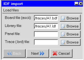
By clicking on the next, the detail for the Import type, XY for the board plane, and Rectangular for the board shape are kept as shown below.
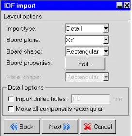
Because the trace information is to be imported later, we do not need to edit the board properties
now. The rest of the details are kept as given below.
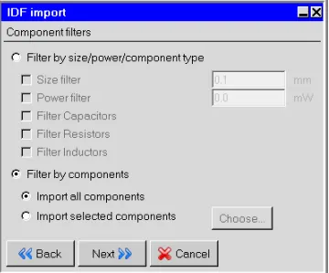
The next is selected to see the Component Models section. Details are kept as shown below:
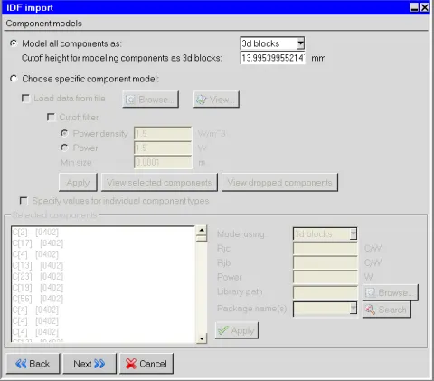
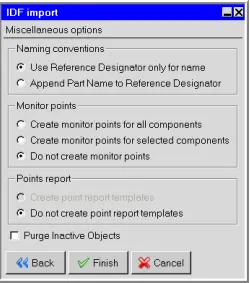
By clicking Next, the Miscellaneous options section is set where the naming and monitor
options are specified. The default options are kept and the Finish was clicked to start importing the files.
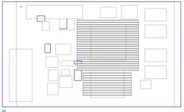
. The A11.tzr file is unpacked to the desktop and the project was named “A11".
The imported A11 board layout.
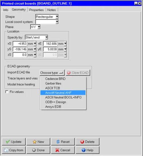
by right-clicking on the BOARD_OUTLINE.1 located in the board assembly in the Model Manager window
The Printed circuit boards object panel was displayed to edit.
To import the trace layout, the procedures are followed as given below:
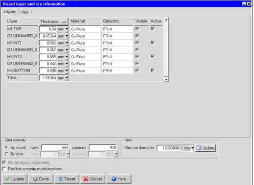
The number of layers in the board is automatically imported to ANSYS Icepak, and the thickness of each layer and the type of the material are entered as mentioned in the problem. The metal
layers are pure Cu and the dielectric layers are FR-4.
Importing Trace Layout and Editing Layer Information
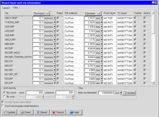
Via information is imported automatically.
Vias Information
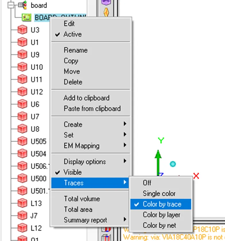
Displaying Traces on the Board by following the procedure given below:
Trace Layout on the PCB with the Color by trace Option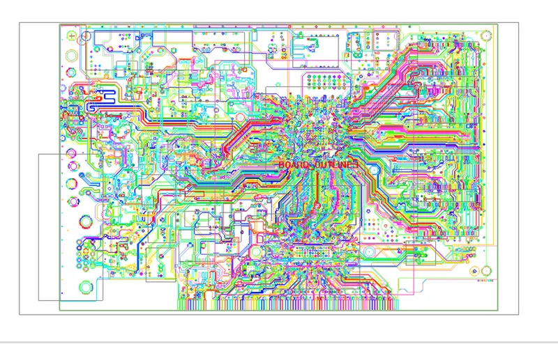
Displaying Trace Layers:
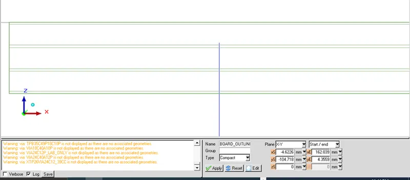
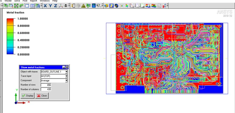
In the Show metal fractions panel, the BOARD_OUTLINE.1
across from an Object with traces is selected. The other fields are automatically filled with the PCB information.
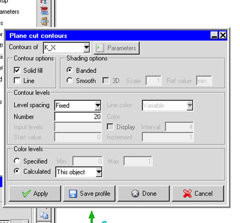
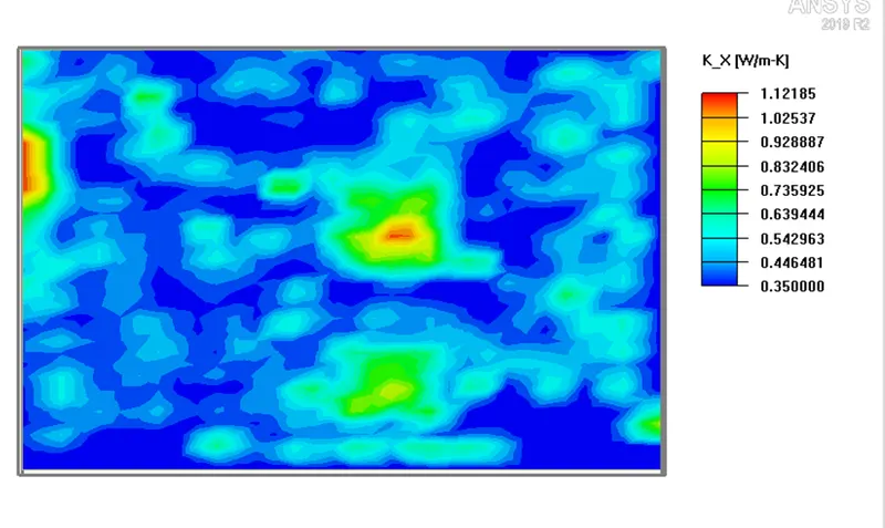
Metal fractions display
Mesh Generation
All objects (including the openings) are made inactive except the BOARD_OUTLINE.1 object.
For the cabinet, the Autoscale from the Edit window is selected to make the size of the board and the cabinet the same.
The properties of the cabinet are changed as shown below:
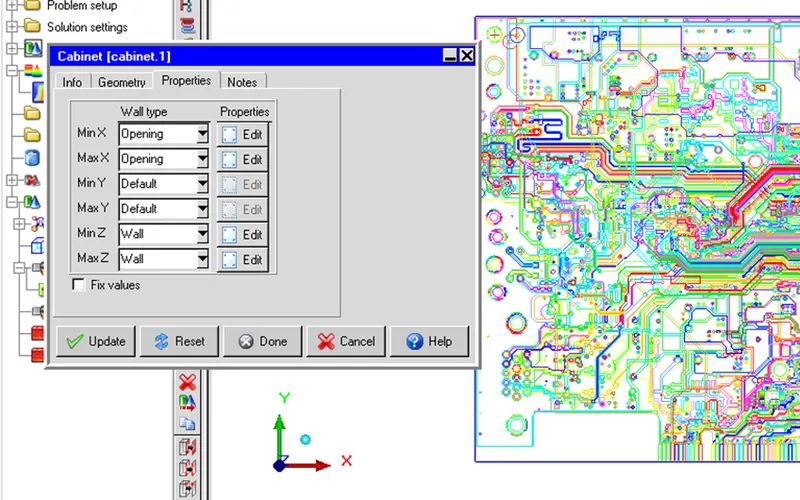
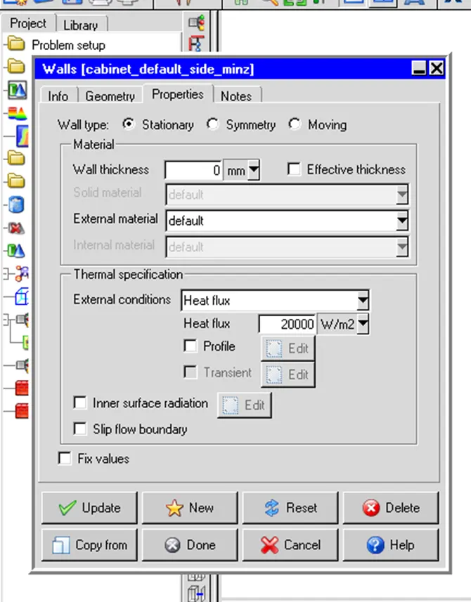
The rest of the sides are insulated. The board will be simulated using a conduction-only model.
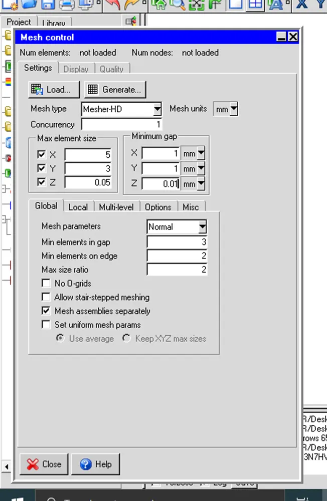
By clicking on Generate Mesh to open the Mesh control panel, details are filled in as given below:
The quality of mesh for conduction-only analysis, in terms of face alignment, volume, and skewness is given below:
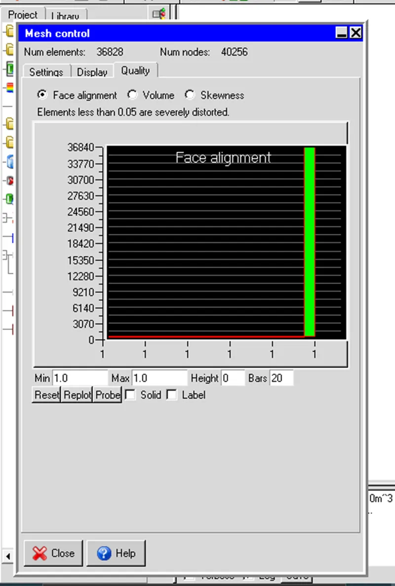
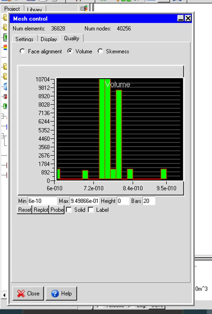
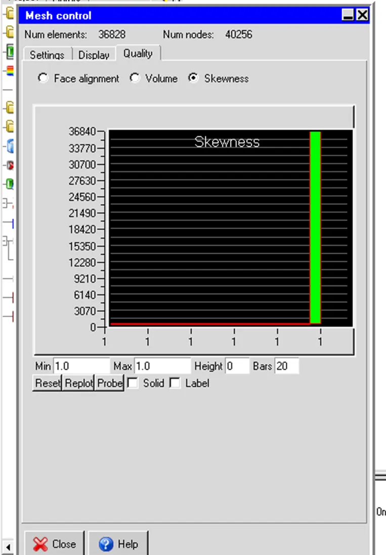
Setting the Physical and Numerical Values as given below:
Since this is a conduction-only model, the Flow option is toggled off in the General setup tab.
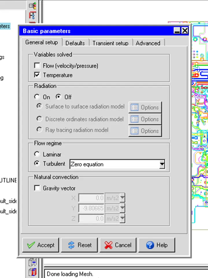
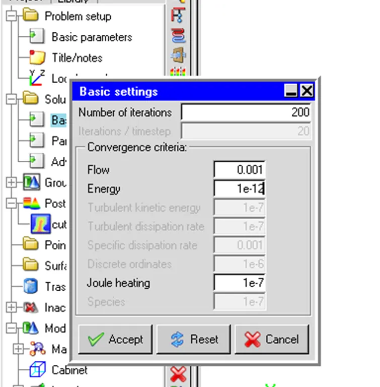
The Number of iterations is set to 200 and the Convergence criteria for Energy is set to 1e-12.
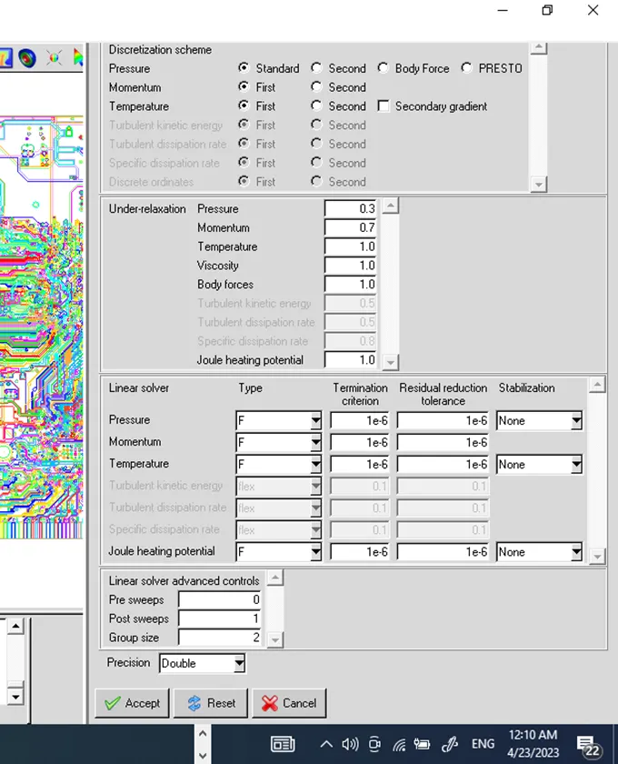
For the advanced solution settings, for Temperature in the Linear solver group box, the F cycle is selected for Type, 1e-6 for both the Termination criterion and Residual reduction tolerance.
After advanced settings project is saved and the solution is run.
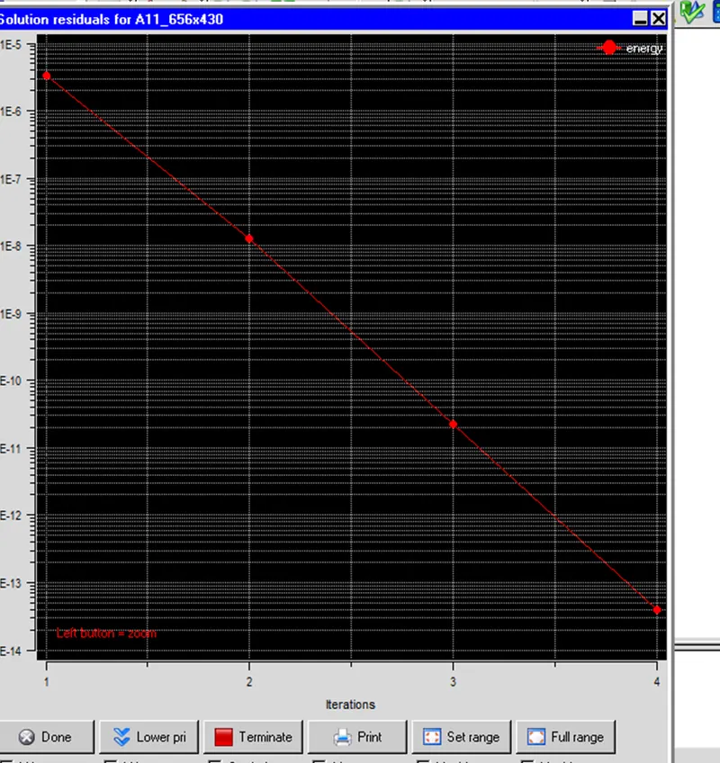
The solution residuals plot for energy is given below
Results:
Temperature Distribution on the PCB (mid-plane)
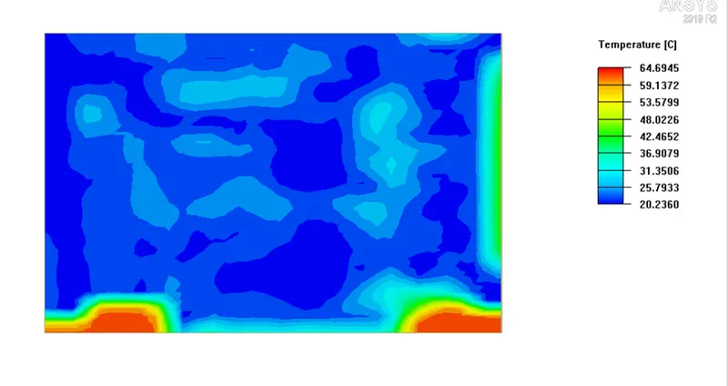
The mid-plane temperature distribution shows that the high-temperature regions occur in the no-trace areas and low-temperature regions occur in areas with a high trace concentration. This is expected as the copper content is directly proportional to the trace concentration. It is worth noting that if a compact or detailed PCB was used instead of the traced PCB, one would obtain a fixed temperature for the entire mid-plane and this fixed temperature would be different from the average temperature of the traced PCB on the same plane.
2. Forced Convection Analysis
To put the actual components back into the model, all the components under the Inactive folder are selected and dragged back into the Model folder. The two wall objects created for the “conduction only" model are selected and dragged into the Inactive folder.
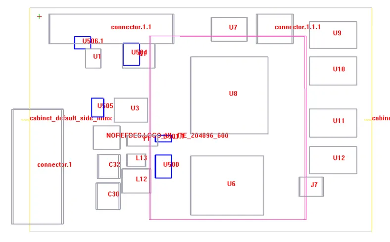
The Cabinet is double-clicked, and then the Autoscale command is selected from the Edit window to fit all the active components into the cabinet.
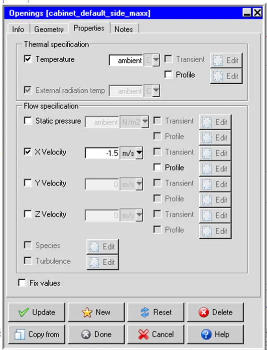
The X Velocity of -1.5 m/s in the Properties tab of the Openings panel for the Max x side of the cabinet is assigned (the minus sign shows that the flow is in the negative x direction).
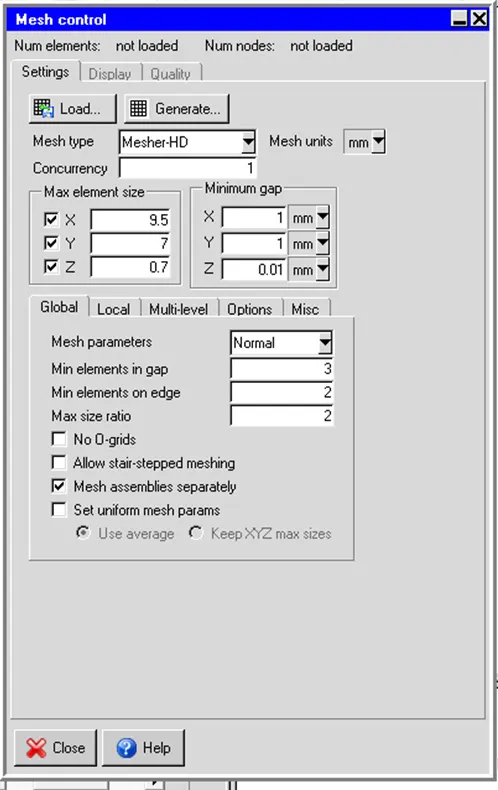
The Mesh control panel is opened, and X, Y, and Z sizes 9.5, 7, and 0.7 mm, are filled respectively.
The rest of the details are kept as default.
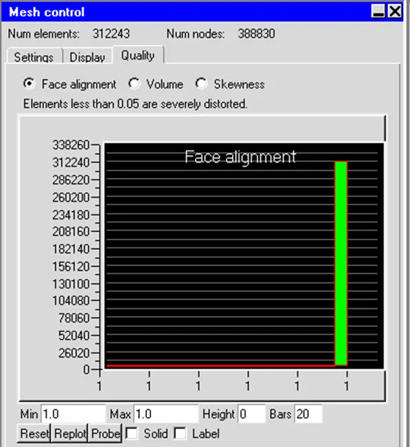
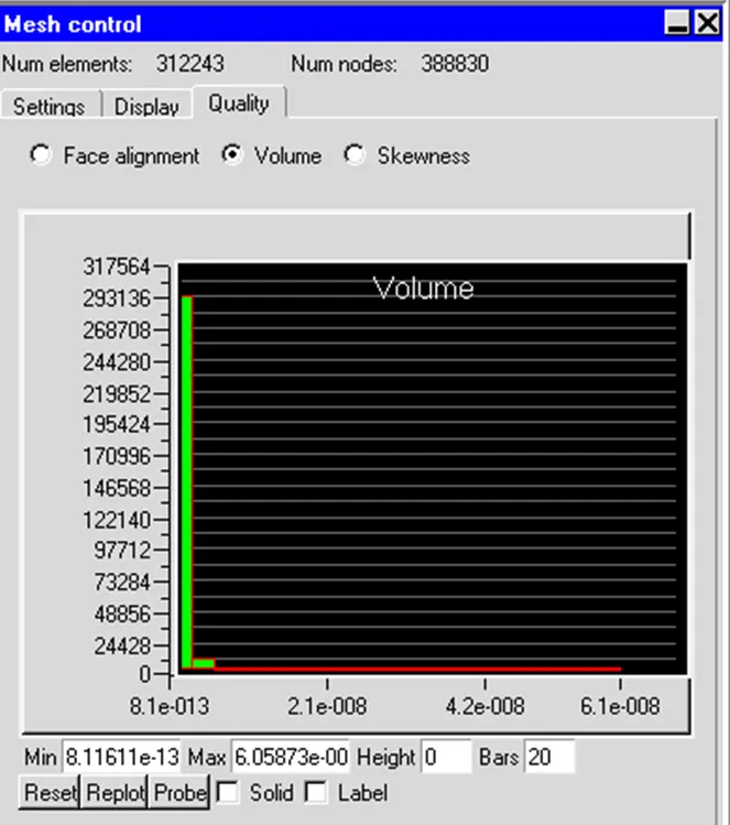
Mesh is generated and mesh qualities in terms of face alignment, volume, and skewness are given below:
Setting the Physical and Numerical Values
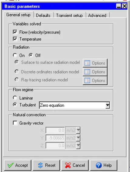
Since it is forced convection, the Flow button in the problem Setup Basic parameters is toggled on. The Turbulent and Zero equation for the flow regime is chosen.
From the Solution setting, in the Basic settings, the number of iterations is set to 300
The convergence criteria are kept the same as shown below:
The Advanced settings as in the conduction-only case.
Running the Solution.
Sequential solution of flow and energy equations is enabled and
the solution is started.
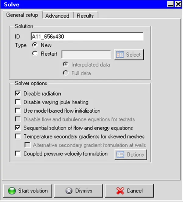
Examine the Results:
To display the contours of temperature on the board, the following procedures are adopted and are given below.
BOARD_OUTLINE.1 from the Object drop-down list is selected for the Object Face temperature contour plot.
For Color levels, This object from the drop-down list is selected.
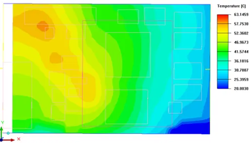
This shows the temperature distribution at the top of the surface of the board. There
are hot spots underneath the high heat flux components.
The temperature contours plot of the forced convection model showed high-temperature regions occurring in the no-trace areas and low-temperature regions occurring in areas
with a high trace concentration.
3. To study Joule Heating
Since the PCB traces have electrical resistance, they heat up as current flows through them. Modeling this
the phenomenon will provide us with an accurate prediction of the temperature distribution in the PCB,
which can be important, for example, in evaluating the performance of the cooling system.
From the File selection panel, the packed project file "Joule-heating.tzr" is selected and clicked to Open.
The project is unpacked in a separate working directory.
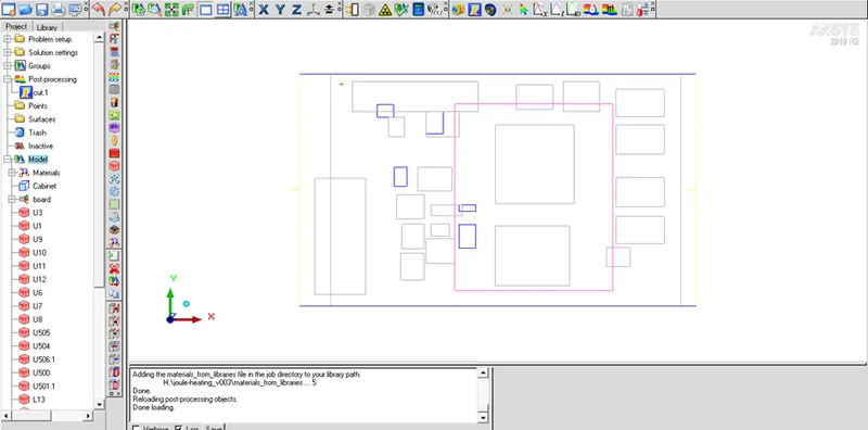
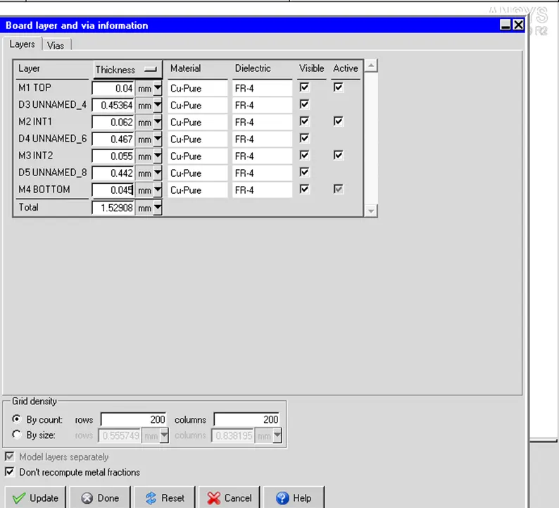
Imported the traces using A1.anf and changed the thickness as described in the problem, Kept the default values for the Grid density.
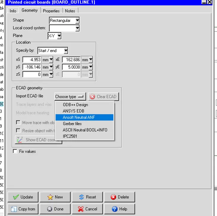
Layer thickness is entered as shown below:
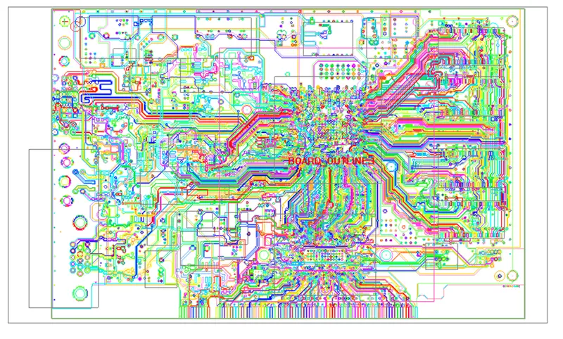
The BOARD_OUTLINE.1 from the Model manager window is selected
By Right clicking on the object BOARD_OUTLINE.1 and again by clicking on Traces in the context menu, the Off is selected to remove the display.
Model Trace Heating is edited as shown below:
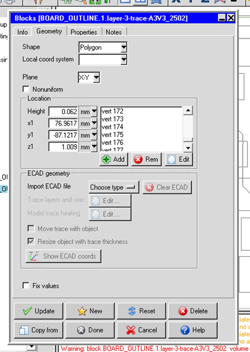
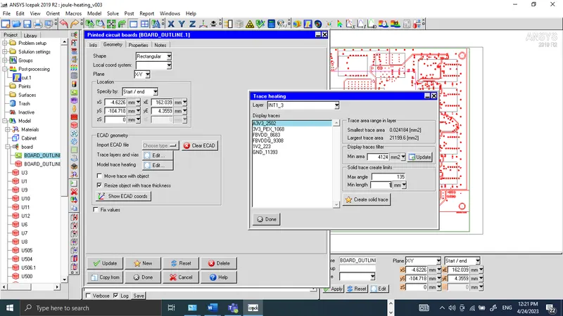 Solid Block Created for the Trace is given below:
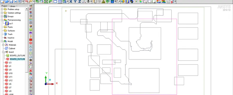
Polygonal Trace Block is opened to edit the material
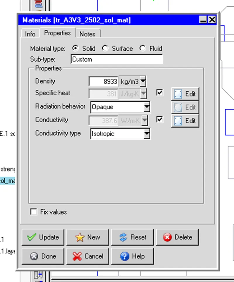
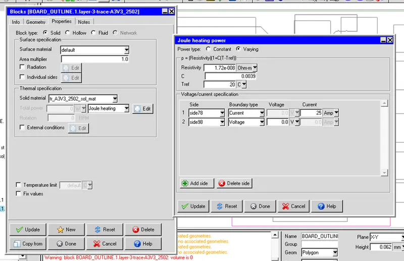
Boundary condition for Joule-Heating is given below:
Creating a non-conformal assembly for the trace:
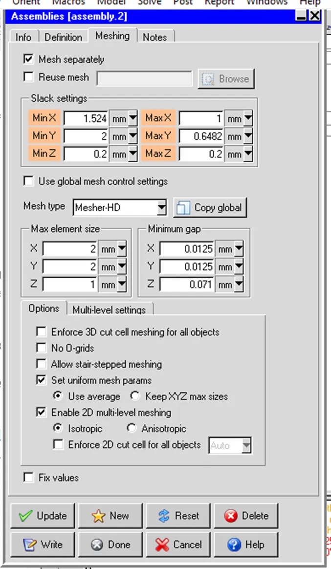
Generating the mesh
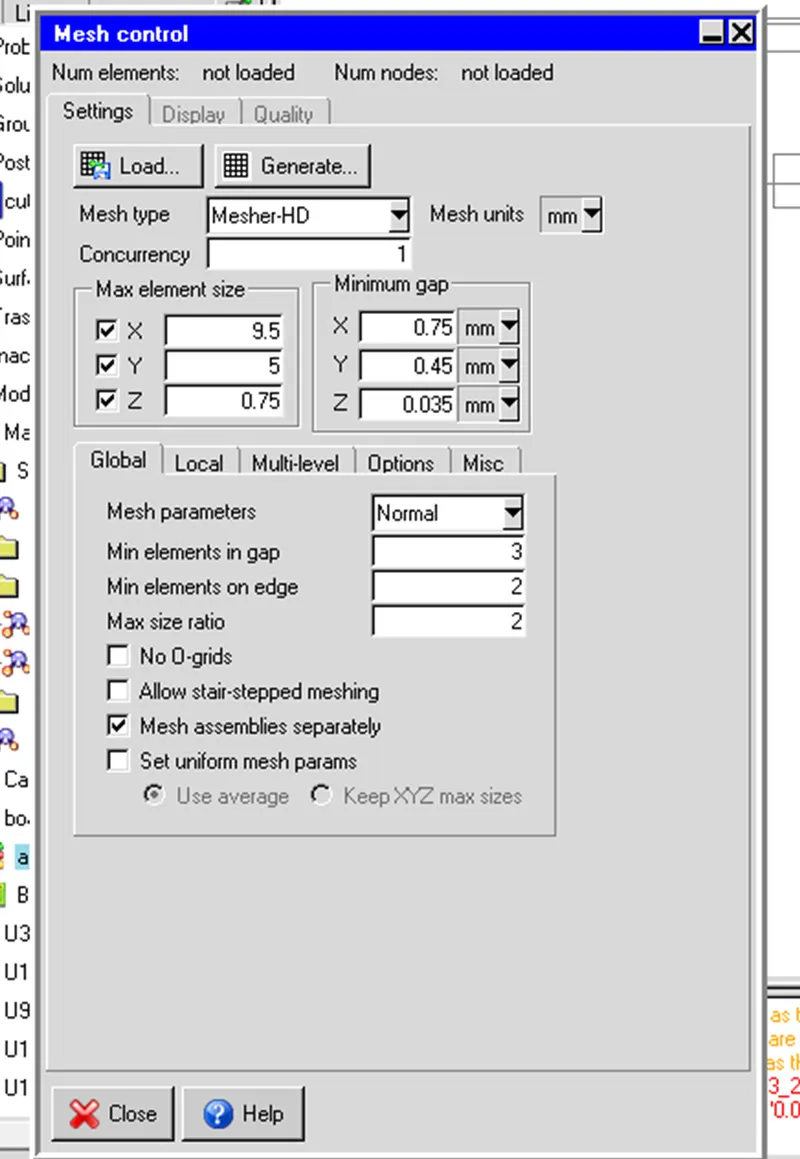
Global obal mesh settings are given below:
Generated mesh quality in terms of face alignment, volume, and skewness is given below:
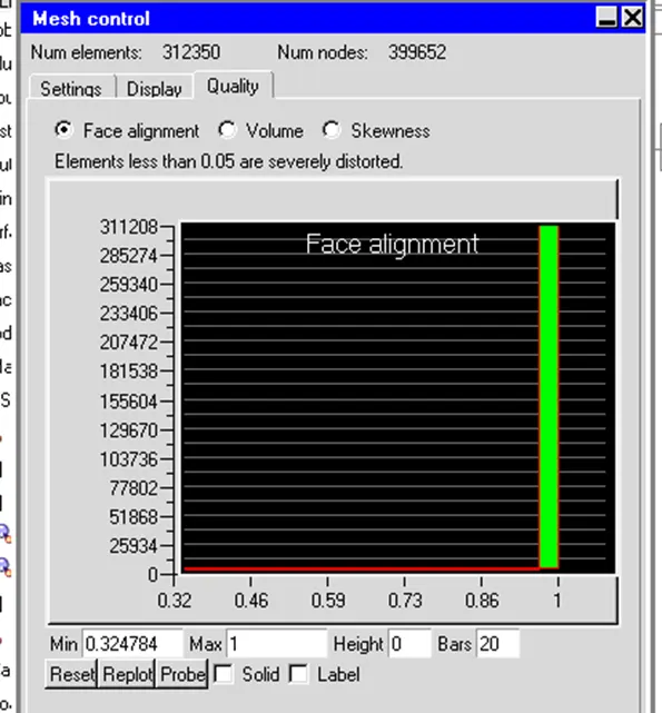
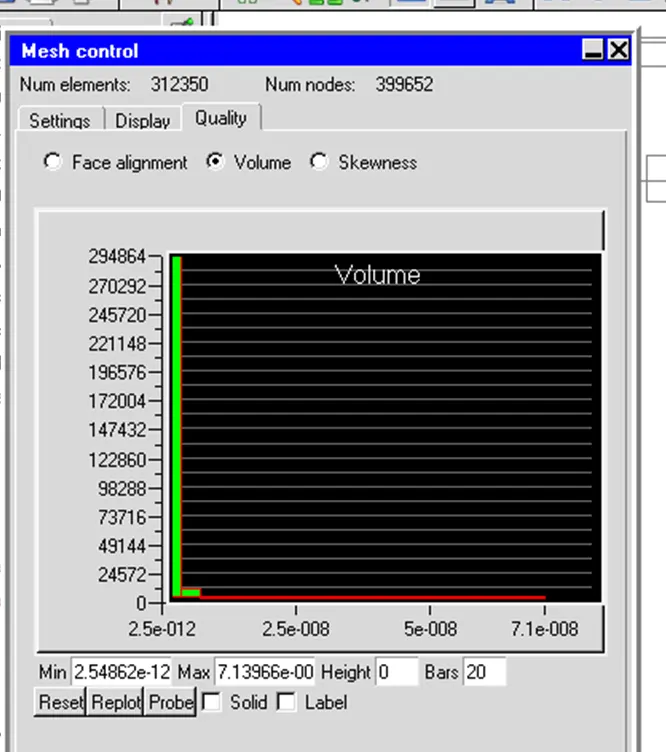
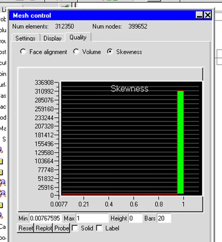
Mesh quality can be further improved but for the first cut solution it can be used.
Physical and Numerical Settings:
The x velocity of the cabinet_default_side_maxx object is set to be -1.5 m/s.
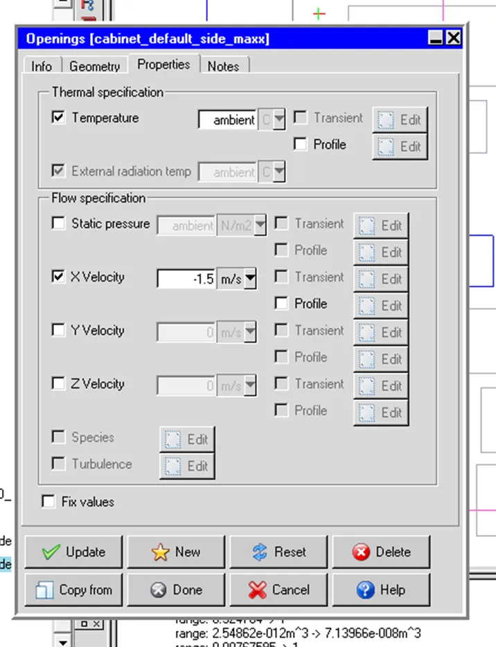
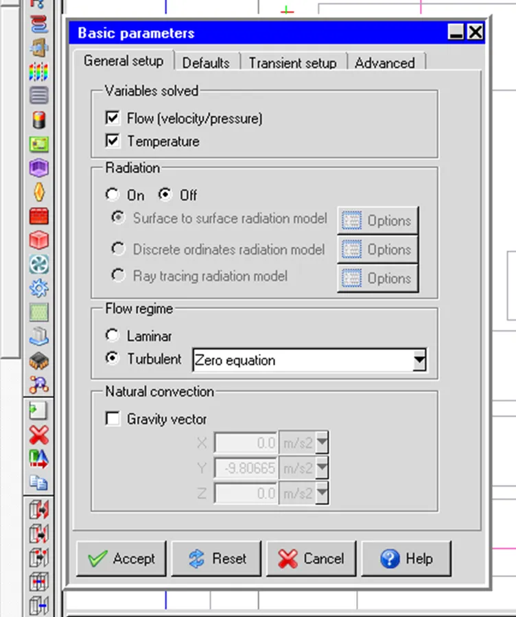
Problem Set Up
Basic Settings are given below:
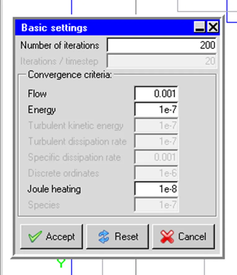
Basic settings for solution are given below:
Adavenced solver selltings are given below:
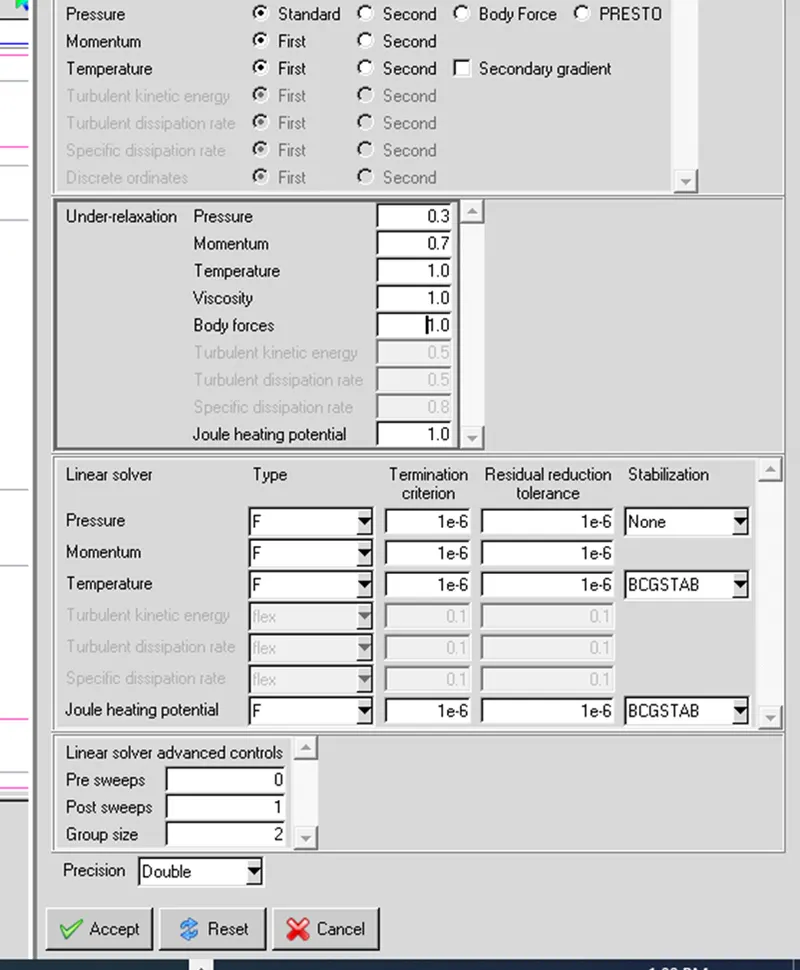
Other data is kept as default.
Project is saved and solution is run.
Solution Residuals are given below:
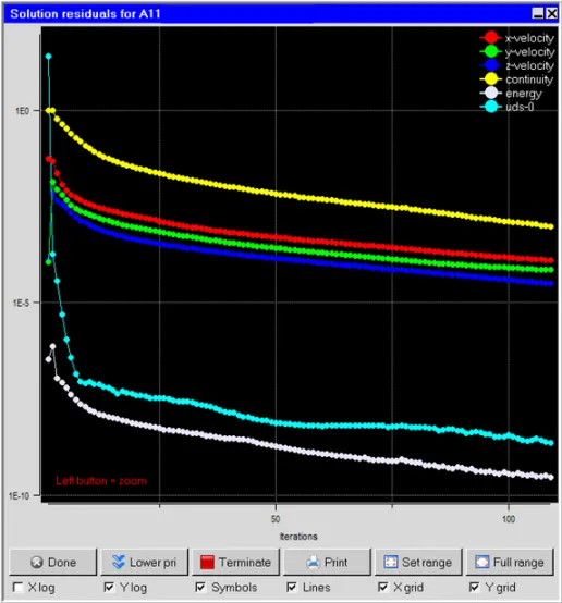
High residuals indicate that the solution has not yet converged and further iterations are needed to obtain accurate results. Conversely, low residuals suggest that the solution has reached convergence, and the results are reliable.
Examine the Results:
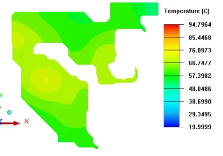
Trace Temperature Contours with Forced Convection is given below:
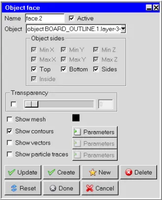
Trace Electric Potential Contours with Forced Convection is given below:
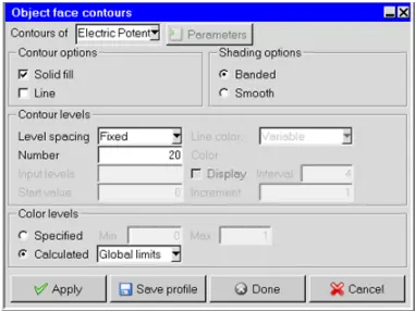
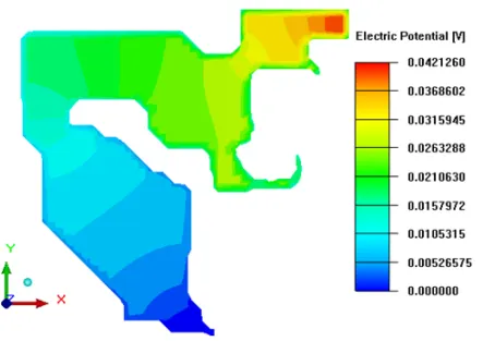
Similarity between the temperature and the electric potential contours can be observed from the above two contours plots.
The temperature contours are closely related to the electric potential contours, which is a direct
result of Joule heating of the trace.
Conclusions:
All the three sections of the given problem, Conduction Only Mode, Forced Convection Mode, and Joule- heating is performed successfully.
The trace layers for a PCB is imported and modeled with various degrees of accuracy and details.
Traces are filtered by their geometry and the Joule heating or resistive heating of desired traces is modeled in ANSYS Icepak.
An accurate prediction of the temperature distribution in a PCB is done successfully.
The temperature contours are closely related to the electric potential contours, which is a direct
result of Joule heating of the trace.