FPGA vs ASIC: Architecture, Design Flow, Cost Break-Even and Jobs
An FPGA is configured after it is made; an ASIC is fixed in the foundry's masks. Here is what is inside each chip, the two design flows side by side, a worked break-even volume, sourced area, speed and power gaps, where each one wins, and what India's chip-design incentives and entry-level FPGA and ASIC roles ask for.

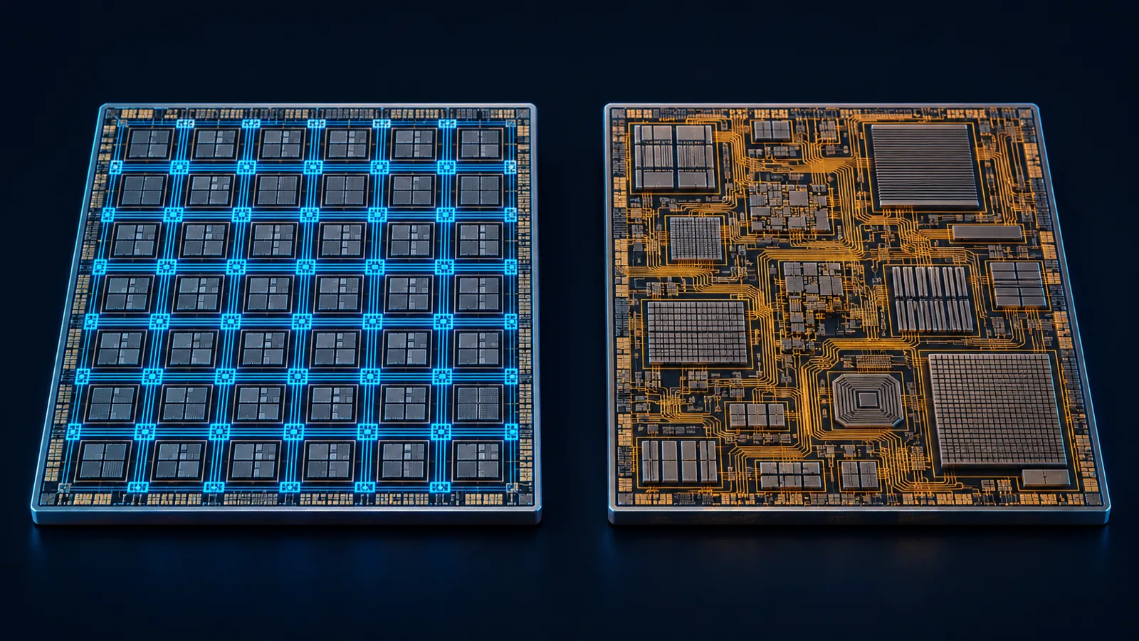
An FPGA (field-programmable gate array) is a chip you configure after it is made: you load a bitstream that sets thousands of small lookup tables, flip-flops and wiring switches into your circuit. An ASIC (application-specific integrated circuit) is a chip whose circuit is fixed in the photomasks at the foundry. FPGAs cost little to start and can be changed at any time, but each unit costs more and uses more silicon and power. ASICs need millions of dollars up front, then win on unit cost, speed and power once volumes are high.
This guide, for electronics and electrical students and freshers, covers what is inside each chip, both design flows, a worked break-even and sourced performance numbers, then India's chip-design incentives and entry-level roles. For the plants behind India's chip push, see our India Semiconductor Mission 2.0 guide.
In short
- In a 90 nm study, an FPGA needed 35 times the silicon area of a standard-cell ASIC for plain logic, ran 3.4 times slower and used 14 times the dynamic power. Hard multipliers and memories cut the area gap to 18 times (Kuon and Rose, IEEE TCAD, 2007).
- One photomask set cost about $1.2 million at 28 nm and $10.5 million at 7 nm in IC Knowledge's 2020 cost model. An FPGA needs no masks of its own.
- In our illustrative example, a 28 nm ASIC becomes cheaper than an FPGA after 61,111 units. One respin moves that to 76,852, and an FPGA at half the price moves it to 137,500.
- Bitcoin mining went from FPGAs to ASICs within about a year: a 130 nm ASIC stick did about 6 times the hashes per joule of a quad-FPGA board (Taylor, IEEE Computer, 2017).
- India's Design Linked Incentive scheme had sanctioned 24 chip-design projects with 16 tape-outs and 6 chips fabricated by January 2026 (PIB, 4 January 2026). Semicon 2.0 now offers seed funding up to ₹15 crore and 9% of net sales for five years for deployed chips (ISM).
What is the difference between an FPGA and an ASIC?
The difference is when the circuit is decided. In an FPGA, the vendor builds a general-purpose grid of logic, memory and wiring, and you decide the circuit later by loading a configuration file. In an ASIC, you decide the circuit first and the foundry builds exactly that, so nothing about the logic can change after fabrication.
Both start as code in a hardware description language such as Verilog, VHDL or SystemVerilog. They part ways at implementation, and that drives everything in the table below.
| Question | FPGA | ASIC |
|---|---|---|
| When is the circuit fixed? | Every time the bitstream is loaded; it can be changed in the field | At tape-out, in the photomasks; a change needs new masks |
| Upfront (NRE) cost | Low: boards, tools and engineering | High: masks ($1.2M per set at 28 nm), design, verification, IP and test |
| Cost per unit | High: you pay for the whole programmable chip | Low at volume: you pay only for the silicon you need |
| Area, speed, power | Worse: 18-35x area, about 3-3.5x delay, 7-14x dynamic power (90 nm study) | Best possible for the job |
| Time to first working hardware | As soon as the design builds and fits | After physical design, signoff, mask making, fab and test |
| Typical fit | Prototypes, low and medium volumes, changing standards | High volumes, battery or thermal limits, peak performance |
What is inside an FPGA?
An FPGA is a grid of configurable logic blocks (CLBs) with columns of block RAM and DSP slices, all joined by programmable routing and ringed by I/O blocks. Configuration memory sets what every block does and which wires connect. Using AMD's 7 series as the example:
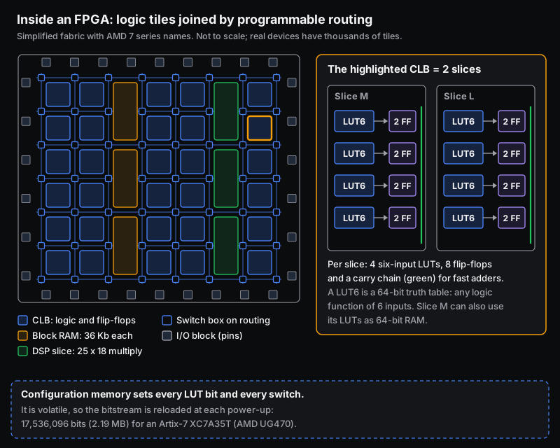
- Lookup table (LUT). A LUT is a tiny memory that stores a truth table. A 6-input LUT holds bits, so it can produce any logic function of its six inputs. AMD's 7 series LUTs can also split into two 5-input LUTs. Our lookup table explainer shows the same idea in software.
- Flip-flops. Each LUT output can be stored in a flip-flop, which is how the FPGA builds registers, counters and state machines.
- Slices and CLBs. In AMD's 7 series, four 6-input LUTs, eight flip-flops, multiplexers and carry logic form a slice, and two slices form a CLB. About two-thirds of slices are logic-only (SLICEL). The rest (SLICEM) can also use their LUTs as 64-bit distributed RAM (AMD UG474).
- Routing. Each CLB connects to a switch matrix that gives it access to the general routing. The switches are set by configuration bits, a big reason an FPGA is larger and slower than fixed wiring.
- Block RAM. Dedicated memory blocks of 36 Kb each, usable as one 36 Kb RAM or two independent 18 Kb RAMs (AMD UG473).
- DSP slices. Hard arithmetic blocks with a 25 x 18 two's-complement multiplier and a 48-bit accumulator (AMD UG479). They make filters and matrix maths far cheaper than LUT-built multipliers.
- Configuration memory. AMD stores configuration in CMOS configuration latches, which lose their contents at power-off. The bitstream is therefore reloaded at every power-up, usually from a flash chip on the board. A small Artix-7 (XC7A35T) needs 17,536,096 bits, about 2.19 MB (AMD UG470).
Other vendors use different names for similar blocks. Chapter 21 of our VLSI design book works through programming a LUT step by step.
What is an ASIC, and what are full-custom, standard-cell and structured ASICs?
An ASIC is a chip designed for one product or job, with its transistors and wiring fixed by the foundry's masks. ASIC types differ in how much is designed from scratch, trading design effort and upfront cost against density and performance.
- Full-custom. Engineers draw some or all transistors and cells by hand. This gives the densest, fastest circuits, at the highest design cost, so it is usually kept for the blocks where it pays off.
- Standard-cell (semi-custom). The usual digital ASIC. Synthesis tools build the design from a foundry library of pre-designed and pre-characterised cells (gates, multiplexers, flip-flops), then place and route them. Every mask layer is still custom to the chip.
- Gate array and structured ASIC. The transistors, or larger pre-built tiles, are made in advance. Only the top wiring layers are customised for each design, so there are fewer custom masks and turnaround is quicker. Intel's eASIC N5X, launched in November 2020, is a modern structured ASIC aimed at FPGA users wanting lower unit cost and power.
The categories follow Michael J. S. Smith's textbook Application-Specific Integrated Circuits (Addison-Wesley, 1997), which also classes FPGAs as "programmable ASICs".
How do the FPGA and ASIC design flows differ?
Both flows start with the same RTL code and simulation. The FPGA flow maps that RTL onto a fabric that already exists and ends in a bitstream you can load the same day. The ASIC flow has to create the physical chip, so it adds test insertion, full physical design, signoff checks, tape-out, mask making, fabrication and silicon test.
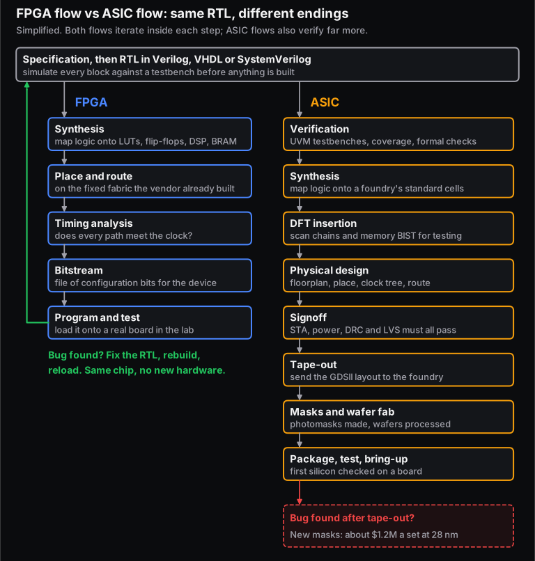
The ASIC-only steps, in plain words:
- Verification at scale. Because a bug in silicon is so expensive, ASIC teams build large SystemVerilog/UVM testbenches, measure coverage and use formal tools before tape-out. FPGA teams can also debug on real hardware.
- DFT (design for test). Every manufactured chip must be tested for fabrication defects. DFT engineers insert scan chains that let a tester shift patterns through every flip-flop, plus built-in self-test for memories. An FPGA vendor has already done this for its chip.
- Physical design. Floorplanning, cell placement, clock-tree synthesis and routing turn the netlist into geometry. On an FPGA, place and route only chooses among existing sites and switches.
- Signoff. Static timing analysis (STA) across process, voltage and temperature corners, power and IR-drop checks, and physical checks: DRC (design rules) and LVS (layout matches the schematic). The foundry will not accept a layout that fails them.
- Tape-out and fab. The final layout (GDSII) goes to the foundry, which makes the masks and processes the wafers. The dies are then packaged and tested, which is the work of an OSAT plant.
Our VLSI design flow guide walks through each ASIC stage in more depth.
How many units before an ASIC is cheaper than an FPGA?
An ASIC becomes cheaper once the money it saves on every unit has paid back its extra upfront cost. With our illustrative inputs, the crossover for a 28 nm ASIC comes at about 61,000 units. The answer moves a long way with the node, the FPGA's price and whether the first silicon works.
Model each option's lifetime cost as a fixed NRE (non-recurring engineering) plus a unit cost per chip. NRE is the one-time spend: masks, design and verification effort, IP licences, EDA tools and test development. Set the two totals equal and solve for the volume:
Worked example (illustrative). Only the 28 nm mask-set cost below is sourced, from IC Knowledge's 2020 model. Every other input is an assumption chosen to show the method, so use your own quotes for a real decision.
| Input | FPGA route | 28 nm ASIC route |
|---|---|---|
| Mask set | none | $1.2M (IC Knowledge, 2020) |
| Design, verification and physical design | $0.4M in total (board, tools, engineering) | $4.0M (assumed) |
| IP licences and EDA tools | $1.5M (assumed) | |
| Test and package development | $0.3M (assumed) | |
| Total NRE | $0.4M | $7.0M |
| Cost per unit | $120 per FPGA (assumed) | $12 per tested, packaged chip (assumed) |
Check: at 10,000 units the FPGA route costs $1.60M against $7.12M for the ASIC. At 200,000 units it costs $24.4M against $9.4M, or $122 against $47 a unit.
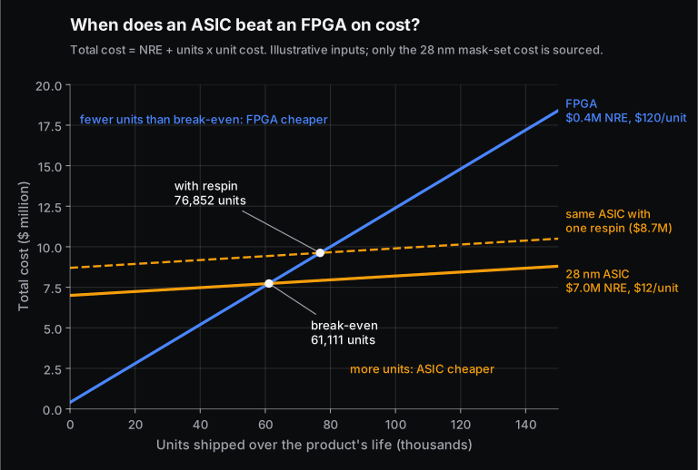
The answer is very sensitive to the inputs:
| Scenario (other inputs unchanged) | ASIC NRE | Break-even |
|---|---|---|
| Base case, 28 nm | $7.0M | 61,111 units |
| One respin: a second mask set plus $0.5M of debug | $8.7M | 76,852 units |
| FPGA at $60 instead of $120 | $7.0M | 137,500 units |
| Design fits a 90 nm node: $165K masks; other costs and $20 a chip assumed | $2.965M | 25,650 units |
For a real example of NRE at an older node: Butterfly Labs' first Bitcoin-mining ASIC in 2012 had about $500,000 of mask NRE on a 65 nm GlobalFoundries process (Taylor, IEEE Computer, 2017). Cost is not the only test: teams also weigh time to market, the risk of the specification changing after tape-out, and power or size limits an FPGA cannot meet.
Is an ASIC faster and more power-efficient than an FPGA?
Yes, for the same function on the same process node. A widely cited measurement compared a 90 nm Altera Stratix II FPGA with 90 nm standard cells. For plain logic the FPGA needed 35 times the area, was 3.4 times slower and used 14 times the dynamic power (Kuon and Rose, IEEE TCAD, 2007). The FPGA's hard multipliers and memories narrow the area and power gaps a lot, but barely change the speed gap.
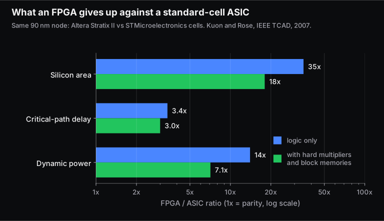
| Metric (FPGA / ASIC) | Logic only | With hard multipliers and memories |
|---|---|---|
| Silicon area | 35x | 18x (the authors estimate it could fall below 5x with heavy use of hard blocks) |
| Critical-path delay | 3.4x | 3.0x |
| Dynamic power | 14x | 7.1x |
| Static (leakage) power | 87x at typical conditions but 5.4x at worst case; the authors call both results of unclear use | |
Read these as orders of magnitude, not today's exact numbers: the study is from 2007 and covers core logic only, not I/O. Modern FPGAs carry many more hard blocks, which narrows the gap for designs that use them. The direction has not changed, because the programmable routing and configuration cells that make an FPGA flexible are what cost area, delay and power.
At the system level, the gap is why specialised ASICs exist. Google's TPU, an inference ASIC used in its data centres since 2015, ran on average 15 to 30 times faster than the CPUs and GPUs of its day, with 30 to 80 times better performance per watt (Jouppi et al., ISCA 2017). That comparison is against processors, not FPGAs, but it shows what fixed, purpose-built silicon buys.
When should you prototype on an FPGA, and what are eFPGA and FPGA-to-ASIC migration?
Prototype on an FPGA whenever software or system testing must start before the ASIC exists, or when the RTL is still changing. ASIC teams map their RTL onto large FPGA boards to boot real software and connect real interfaces before the silicon exists. Synopsys says its HAPS-100 runs complex SoC designs at 20 to 50 MHz for pre-silicon software development (Synopsys blog, April 2021). That is slower than the final chip, but fast enough for software teams to start work.
eFPGA (embedded FPGA) puts a block of FPGA fabric inside an ASIC, so part of the chip can be reprogrammed after fabrication. Typical uses are protocols or algorithms that may change, or one chip serving several customers. QuickLogic, for example, sells eFPGA IP and lists process nodes from 180 nm down to 6/7 nm (vendor page). The programmable block still costs more area and power than fixed logic.
FPGA-to-ASIC migration means taking a proven FPGA design into an ASIC once volumes justify it. A structured ASIC is the halfway step. When Intel launched eASIC N5X in November 2020, it said customers could move FPGA designs, including those using the FPGA's hard processor, onto it for up to 50% lower core power and lower cost than FPGAs (Intel's own claim). A full standard-cell ASIC goes further but repeats the whole ASIC flow. RTL ports more easily if vendor-specific blocks (FPGA RAMs, DSP primitives, clock managers) sit behind wrapper modules that can be swapped for ASIC memories and cells.
Which products moved from FPGAs to ASICs, and which stay on FPGAs?
Products move to ASICs when the algorithm is frozen and volume or energy cost is huge. Bitcoin mining and AI inference are the classic cases. Products stay on FPGAs when standards change, volumes are modest, I/O needs are unusual or the hardware must be updated in the field. Telecom radios, radar and defence electronics, and test instruments are examples.
Moved to ASICs: Bitcoin miners and AI accelerators
Michael Taylor's history of Bitcoin hardware (IEEE Computer, 2017) traces mining from CPUs to GPUs to FPGAs to ASICs. Open-source FPGA miners appeared in June 2011. Quad-FPGA boards built on Spartan-6 chips reached 860 MH/s at 39 W and cost $1,060. ASIC preorders opened in June 2012, and, in Taylor's words, the reign of FPGA miners "was brief".
One early ASIC, a 130 nm USB-stick miner, did 330 MH/s at 2.5 W with a design that mirrored the earlier FPGA pipelines. That is 132 MH per joule against 22.1 MH per joule for the FPGA board, about 6 times better. Once SHA-256 hashing was a fixed job, the FPGA's flexibility had no value. Google's TPU applied the same logic to neural-network inference.
Stay on FPGAs: telecom, defence and test equipment
- Telecom radios. AMD's Zynq UltraScale+ RFSoC puts direct RF-sampling data converters on the same chip as FPGA fabric, and AMD pitches its DFE variant at mass 5G radio deployments. Radio standards and band plans keep changing, so the fabric lets the same hardware take updates.
- Radar and defence. AMD markets the same RFSoC as a single-chip transmit-receive solution for phased-array radar. Defence systems are built in modest volumes and kept in service for a long time. AMD commits to supplying 7 series parts through 2040 and UltraScale+ parts through 2045 (AMD product page).
- Test and measurement. NI's FlexRIO instruments pair a Kintex-7 FPGA module with interchangeable I/O adapter modules. Users program the FPGA in LabVIEW FPGA or VHDL/Verilog to build custom measurements.
- Data centres, sometimes. Microsoft put an FPGA in each of 1,632 servers to speed up Bing's search ranking. Throughput per server rose 95% at the same latency (Putnam et al., ISCA 2014). Because the boards are reprogrammable, updated ranking logic can be loaded without new hardware.
What do ISM 2.0 and the DLI scheme mean for FPGA and ASIC work in India?
India's chip-design incentives pay mainly for ASIC design and for getting designs to silicon, with FPGAs used along the way for prototyping and validation. The Design Linked Incentive (DLI) scheme has run since December 2021. Semicon 2.0, the second phase of the India Semiconductor Mission (ISM 2.0), is a ₹1,27,500 crore programme whose first pillar is chip design.
DLI under the Semicon India Programme (PIB backgrounder, 4 January 2026):
- Startups and MSMEs get up to 50% of eligible design spending back, capped at ₹15 crore per application, plus 6% to 4% of net sales for five years once the chip sells, capped at ₹30 crore.
- C-DAC's ChipIN Centre provides an EDA tool grid, IP cores, multi-project wafer (MPW) runs, where several designs share one mask set, and post-silicon validation. About 1 lakh engineers and students in 400 organisations use its tools.
- Results: 24 projects sanctioned, 16 tape-outs and 6 chips fabricated. Supported firms include Vervesemi (motor-control chips), InCore (RISC-V processor IP) and Netrasemi (AI chips for CCTV).
Semicon 2.0's design pillar (ISM scheme page, last updated 6 November 2026) offers startups and MSMEs seed funding of 50% of project cost or ₹15 crore, whichever is lower, plus equity co-investment. New chips and IP earn 9% of net sales for five years, capped at ₹30 crore per application and ₹120 crore per company. EDA, MPW and validation support continues.
For students, this means more Indian teams taking chips through the full ASIC flow and needing RTL, verification, physical design and post-silicon validation engineers. The Chips to Startup (C2S) programme aims to train 85,000 chip designers (PIB). Our list of companies hiring embedded and VLSI engineers covers who recruits.
What skills do entry-level FPGA and ASIC roles need?
All four common entry roles start from the same base: digital logic, Verilog or SystemVerilog, and timing (setup, hold and clock domains). They then diverge. FPGA engineers add vendor tools and board bring-up. ASIC RTL engineers add synthesis and lint. Verification engineers add UVM. Physical design engineers add place-and-route, STA and scripting.
| Role | What you do | Skills and tools to show | A project that proves it |
|---|---|---|---|
| FPGA design engineer | RTL, constraints, timing closure and lab debug on real boards | Verilog/VHDL, AMD Vivado or Intel Quartus, timing constraints, logic analysers, some C for soft or hard processors | A UART or SPI controller plus a small DSP filter running on a low-cost board, meeting timing |
| ASIC RTL design engineer | Micro-architecture and synthesizable RTL for ASIC blocks | SystemVerilog, FSMs, pipelining, clock-domain crossing, lint, synthesis basics | A pipelined block (a FIFO with CDC, or a small RISC-V core) with documented trade-offs |
| Design verification (DV) engineer | Testbenches, coverage and bug hunting before tape-out | SystemVerilog, UVM, assertions, functional coverage, scripting | A UVM testbench with coverage for an open-source IP block |
| Physical design (PD) engineer | Floorplan, place and route, clock tree and timing closure | STA, Tcl, Linux, PnR concepts, DRC/LVS basics | Take a small RTL block through synthesis, PnR and STA, and explain each timing fix |
To start, build digital-logic fundamentals with our Basics of Digital Electronics course. Embedded C and microcontrollers, which FPGA and post-silicon work also use, are covered in Fundamentals of Embedded Systems. For role details and pay, read VLSI engineer job roles and VLSI career and salary prospects in India. Then practise with our VLSI interview questions.
What is the catch?
The cost example is a method, not a price list. Only the mask-set costs come from a published model, and those are 2020 figures for one fab scenario. Real NRE depends on the design's size, its IP and its team, and FPGA prices vary widely by part and volume.
The performance gaps come from one careful 2007 study at 90 nm: they show direction and rough size, not today's ratio for any given chip. Vendor figures quoted here (Intel's power claim, Synopsys's prototype speeds, QuickLogic's node list, AMD's supply dates) are the companies' own statements.
And the choice is often not either-or. Products ship on an FPGA first and move to an ASIC later, pair an ASIC with a small FPGA, or embed FPGA fabric in the ASIC.
Frequently asked questions
Is an FPGA better than an ASIC?
Neither is better in general. An FPGA is better when you need hardware quickly, expect changes, or ship in modest volumes. An ASIC is better when the design is stable and volume is high, or when power, size or speed limits rule out an FPGA. Many products start on an FPGA and move to an ASIC.
Can an FPGA design be converted into an ASIC?
Yes. The RTL can be re-synthesised to a foundry's standard cells, but the design must then go through the full ASIC flow: verification, DFT, physical design, signoff and tape-out. Vendor-specific FPGA blocks such as RAMs, DSP slices and clock managers must be replaced. A structured ASIC such as Intel's eASIC is a shorter path.
Is the same Verilog used for FPGA and ASIC?
Mostly. Both use synthesizable Verilog, VHDL or SystemVerilog. The differences are in the details: FPGA code often infers or instantiates vendor RAMs and DSP blocks, and relies on flip-flops starting at known values after configuration. ASIC code needs explicit resets, test-friendly structures and foundry memories.
Should a fresher in India learn FPGA or ASIC design first?
Learn RTL design and timing first, because both paths need them. Then use a low-cost FPGA board, because it gives you working hardware to show at interviews. After that, choose ASIC verification, RTL or physical design based on the roles you target.
Sources and further reading
- AMD, UG474 7 Series FPGAs Configurable Logic Block User Guide, v1.9, 1 April 2025.
- AMD, UG473 7 Series FPGAs Memory Resources, v1.14, 3 July 2019.
- AMD, UG479 7 Series DSP48E1 Slice, v1.10, 27 March 2018.
- AMD, UG470 7 Series FPGAs Configuration User Guide, v1.17, 5 December 2023.
- I. Kuon and J. Rose, Measuring the Gap Between FPGAs and ASICs, IEEE Transactions on CAD, 26(2), February 2007.
- S. Jones (IC Knowledge), Lithovision 2020 presentation, mask-set costs from the IC Knowledge Strategic Cost Model 2020.
- M. B. Taylor, The Evolution of Bitcoin Hardware, IEEE Computer, September 2017.
- N. P. Jouppi et al., In-Datacenter Performance Analysis of a Tensor Processing Unit, ISCA 2017.
- A. Putnam et al., A Reconfigurable Fabric for Accelerating Large-Scale Datacenter Services, Microsoft Research, ISCA 2014.
- Intel, First Intel Structured ASIC for 5G, AI, Cloud and Edge Announced, 17 November 2020.
- J. Stahl, FPGA Prototyping Powers the SoC Design and Verification Process, Synopsys blog, 14 April 2021.
- QuickLogic, eFPGA IP, product page (accessed 22 November 2026).
- AMD, Zynq UltraScale+ RFSoC, product page (accessed 22 November 2026).
- NI, What Is NI FlexRIO? (accessed 22 November 2026).
- M. J. S. Smith, Application-Specific Integrated Circuits, Addison-Wesley, 1997, chapter 1.
- PIB, Design Linked Incentive Scheme: Catalyzing India's Semiconductor Design Ecosystem, 4 January 2026.
- India Semiconductor Mission, Semicon 2.0 scheme page, last updated 6 November 2026.