Semiconductor OSAT in India: Packaging Steps, Yield Maths and Plants
A semiconductor SEZ for chip packager ASIP was notified in Visakhapatnam on 10 November 2026 (reported), days after the Semicon 2.0 portal opened. Here is what an OSAT does after the wafer leaves the fab, why it tests dies before packaging them (worked yield and cost maths), where India's nine approved OSAT/ATMP plants stand, and the jobs they create for mechanical, electrical and electronics graduates.

Semiconductor OSAT in India means the plants that turn finished silicon wafers into chips you can solder onto a circuit board. Every Indian chip plant in commercial production today is one of these assembly and test units, not a wafer fab. The latest step came on 10 November 2026, when the Commerce Ministry notified a semiconductor SEZ in Visakhapatnam for ASIP Technologies, according to India Briefing.
This guide, written for engineering students, explains each step after the wafer leaves the fab, works through the yield and cost maths behind one key decision, lists India's approved OSAT/ATMP projects with verified status, and maps the roles open to mechanical, electrical and electronics graduates. For the wafer fabs, the ISM 2.0 scheme as a whole and VLSI pay, see our India Semiconductor Mission 2.0 guide. For the machines that make chips, see our semiconductor equipment manufacturing guide. This post doesn't repeat either.
In short
- An OSAT (outsourced semiconductor assembly and test) plant takes finished wafers from a fab, tests and cuts out each chip, packages it and tests it again. India's scheme documents call this ATMP.
- On 10 November 2026 the Commerce Ministry notified a 12.14 ha semiconductor SEZ at Anandapuram, Visakhapatnam, for ASIP Technologies, the OSAT firm. This is reported by India Briefing (13 November); we could not find the gazette copy online.
- The Semicon 2.0 portal opened on 6 November 2026 (PIB). It pays packaging plants 35% of eligible capex for advanced packaging and 25% for legacy packaging, with a minimum investment of ₹1,000 crore (ISM scheme page).
- India has approved nine OSAT/ATMP units. Five are in commercial production: Micron, Kaynes and CG Semi in Sanand, CDIL in Mohali and Suchi in Surat. Tata's Jagiroad plant in Assam has reported pilot production.
- Our worked example: with a $10 package, probing dies before packaging cuts the cost per good chip from $19.15 to $18.41. In a four-die package, untested dies leave only 67% of packages fully good.
What is OSAT, and is it the same as ATMP?
OSAT stands for outsourced semiconductor assembly and test: a company that packages and tests chips designed or fabricated by someone else. ATMP (assembly, testing, marking and packaging) describes the same back-end work, including plants owned by the chipmaker itself. Micron's Sanand plant is an ATMP unit because it handles Micron's own memory. CG Semi's is an OSAT.
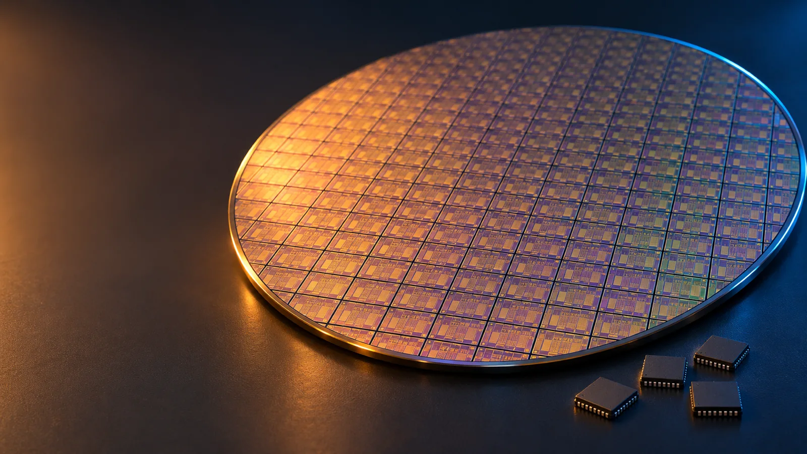
A chip's life has two halves. The front end is the fab, where transistors and wiring are built layer by layer on a silicon wafer. The back end starts when that finished wafer arrives at the OSAT. A bare die is brittle, sensitive to moisture and has pads far too small to solder to a board. The package gives it a body, a heat path and pins or balls a circuit board can use. Think of the fab as a printing press that turns out sheets of postage stamps, and the OSAT as the line that checks each stamp, cuts it out, laminates it and files it.
What happened in Visakhapatnam on 10 November 2026?
On 10 November 2026 the Union Ministry of Commerce and Industry notified a 12.14-hectare special economic zone (SEZ) for Advanced System In Package Technologies (ASIP), an OSAT firm. India Briefing reported this on 13 November 2026, citing notification S.O. 6148(E). It gives the site as 11.26 ha at Tarluwada plus 0.877 ha at Gidizala in Anandapuram, after a letter of approval on 19 October 2026. The zone is also an inland container depot, so goods can clear customs on site. No investment figure is stated.
Confirmed vs reported. The notification is reported: we could not find S.O. 6148(E) on the SEZ India website or by web search on 17 November 2026. The project is confirmed. The Cabinet approved ASIP's unit on 12 August 2025, with technology from APACT of South Korea and a capacity of 96 million units a year (PMO), at ₹468 crore (PIB). ISM records a financial support agreement (FSA) with ASIP signed in October 2026.
Deccan Chronicle reported that the Prime Minister laid the foundation stone virtually on 1 August 2026 for a 30-acre site, with wire-bond and flip-chip BGA packaging first and 2.5D/3D within two to three years (no official release found). As a cross-check, 30 acres is 12.14 ha, the notified SEZ area.
Four days earlier, on 6 November 2026, the electronics ministry opened the Semicon 2.0 portal for pillar 2 (machines and materials), pillar 3 (fabs) and pillar 4 (ATMP/OSAT) (PIB).
What does Semicon 2.0 pay a new OSAT plant?
Pillar 4 of Semicon 2.0 pays 35% of eligible capital expenditure for advanced packaging and advanced substrates, and 25% for legacy packaging. It is paid pari-passu, in step with the company's own spending. An applicant needs at least ₹1,000 crore of investment and ₹200 crore of revenue, and must own or license production-grade technology (ISM, Semicon 2.0 scheme page).
Advanced means 2.5D/3D, wafer-level chip-scale packaging, heterogeneous integration and advanced substrates; everything else is legacy. Support is released over six years, and applications stay open for three years from the guidelines of 16 September 2026.
Worked example. Take a plant with ₹1,200 crore of eligible capex (figures in ₹ crore):
In the first phase, Micron said it would get 50% of project cost from the Centre plus 20% from Gujarat (Micron, 22 June 2023); 50% of ₹1,200 crore would be ₹600 crore. Round two pays less, and the 10-point gap pushes firms towards advanced packaging.
What happens to a chip after the wafer leaves the fab?
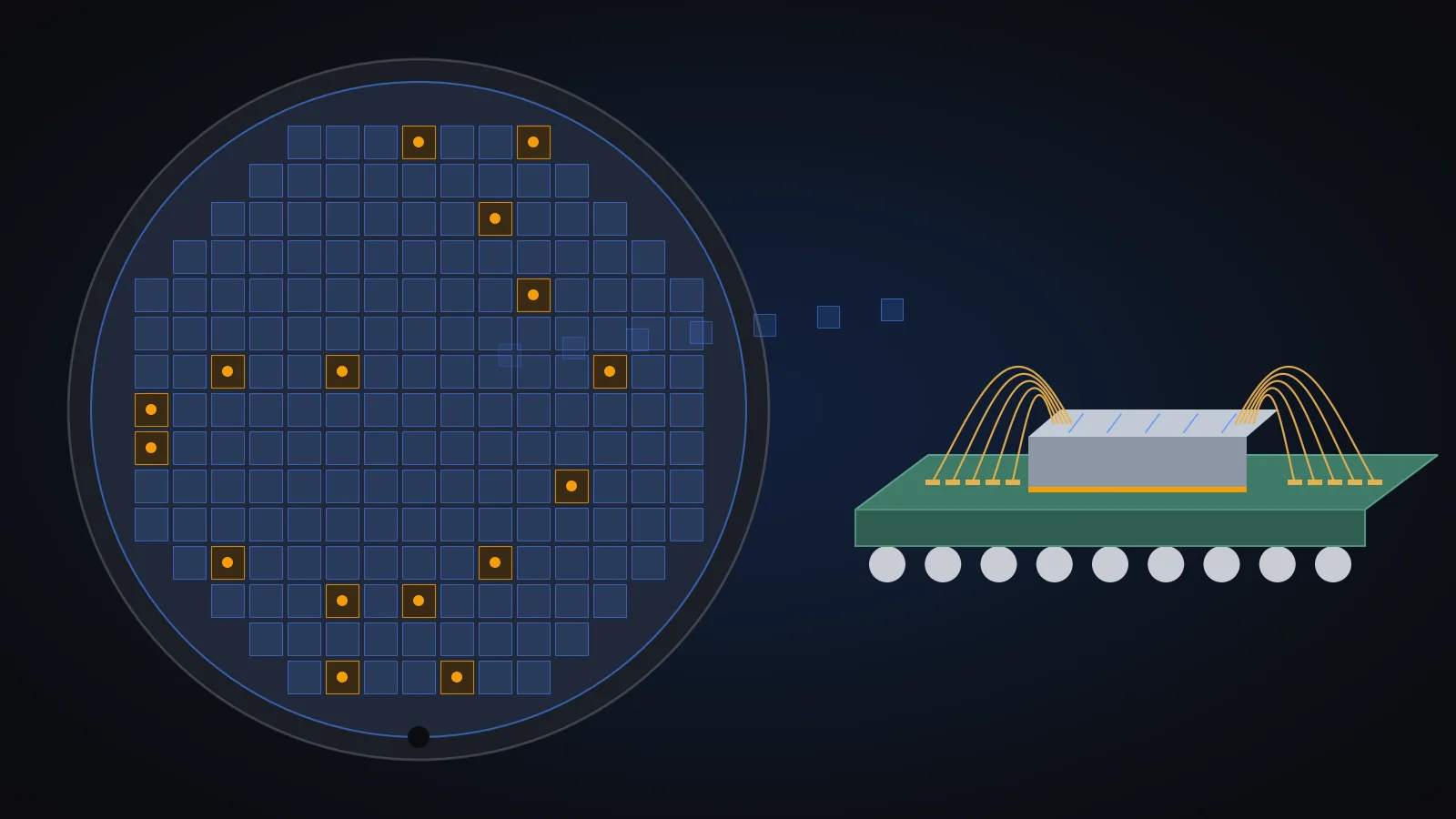
A finished wafer goes through about ten steps at an OSAT: every die is probe-tested, the wafer is thinned and cut, each good die is attached and connected by wires or bumps, then moulded, marked, finished, separated and tested again before shipping.
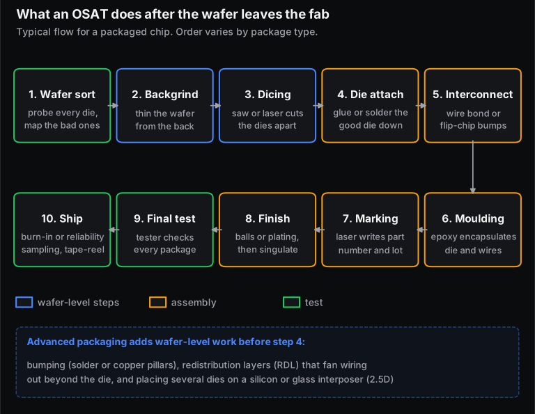
- Wafer sort (probe test). A probe card, a board of fine needles, touches each die's pads while an automated tester runs electrical tests. Failing dies go into a wafer map so they are never packaged.
- Backgrind. The wafer is ground thinner from the back so packages can be thin and memory dies can be stacked. In 2.5D work this step also exposes the through-silicon vias (TSVs), vertical copper links through the die.
- Dicing. A diamond saw or laser cuts along the streets between dies while the wafer sits on stretchable tape. In DISCO's Stealth Dicing the laser forms a modified layer inside the silicon and stretching the tape splits the dies, a narrow, dry cut.
- Die attach. A pick-and-place machine bonds each good die to a lead frame or substrate with epoxy, solder or sintered silver. In power devices this joint is the main heat path.
- Interconnect. Wire bonding or flip chip, compared below.
- Moulding. Epoxy compound is moulded around the die under heat and pressure.
- Marking. A laser writes the part number and lot code for traceability.
- Finish and singulation. BGA packages get solder balls; leaded packages are plated, trimmed and formed. The strip is cut into single units.
- Final test. Handlers feed every package to an automated tester that checks function, speed and power and bins the parts. It catches dies damaged in assembly.
- Burn-in, reliability and shipping. High-reliability parts may be run hot under power (burn-in), and samples face stress tests such as JEDEC temperature cycling (JESD22-A104). Parts ship on tape and reel.
Most of these steps are mechanical, thermal or materials problems: grinding force that cracks a thin wafer, bond force in a wire bonder, warpage of a moulded strip as it cools. That is why OSATs hire mechanical and production engineers as well as electronics engineers.
Wire bond or flip chip: what is the difference?
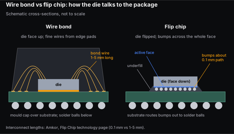
In wire bonding the die sits face up and fine metal wires, 1 to 5 mm long, run from pads around its edge to the package. In flip chip the die is turned face down onto bumps spread across its whole surface, so the electrical path is only about 0.1 mm. Flip chip is faster and handles more connections. Wire bond is cheaper and more flexible.
| Question | Wire bond | Flip chip |
|---|---|---|
| Where are the connections? | Pads around the die's edge only | Bumps over the whole die face (an "area array") |
| Path length | 1-5 mm of wire | About 0.1 mm of bump |
| Electrical effect | More inductance, which limits very fast signals | Lower inductance; power fed straight into the die's core |
| Wire or bump metal | Gold, or cheaper copper, palladium-coated copper or silver alloy | Solder bumps or copper pillars with a solder cap |
| Typical use | Microcontrollers, analog, power and memory parts in leaded, QFN or wire-bonded BGA packages | Processors, high-speed and RF chips in flip-chip BGA or chip-scale packages |
| Extra steps | None beyond bonding | Wafer bumping before dicing; underfill after attach to protect the joints from thermal stress |
Sources: Amkor's flip chip, copper pillar and interconnect pages. A note for mechanical engineers: silicon and an organic substrate expand at very different rates, so every power cycle bends the bumps a little. Underfill, an epoxy wicked under the die, locks the two together and spreads that strain, which is why solder-joint fatigue analysis is a core package CAE job. Solder itself is applied eutectic phase-diagram knowledge, covered in our interactive Engineering Materials and Metallurgy book.
What is advanced packaging (fan-out, 2.5D and 3D)?
Advanced packaging puts more connections, or several dies, into one package by doing package wiring at wafer scale. Fan-out spreads wiring beyond the die's edge. 2.5D places dies side by side on a silicon or glass interposer. 3D stacks dies vertically and connects them with through-silicon vias. Semicon 2.0 pays 35% for this category against 25% for legacy packaging.
- Wafer-level chip-scale package (WLCSP): balls go straight onto the die on the wafer, so the package is no bigger than the chip.
- Fan-out wafer-level packaging: dies are moulded into a "reconstituted" wafer and redistribution layers carry wiring beyond the die's edge. Amkor says it has shipped over 2 billion units of one fan-out type, eWLB.
- 2.5D: dies such as a processor and memory stacks sit side by side on a finely wired interposer, usually silicon; 3D Glass Solutions plans glass ones in Bhubaneswar.
- 3D and heterogeneous integration: dies are stacked, or chips from different processes are combined in one module ("chiplets").
In India, Tata's Assam unit lists flip chip and integrated system-in-package (PIB, 29 February 2024), and 3D Glass Solutions plans glass interposers with silicon bridges and 3D modules (PMO, 12 August 2025). ASIP's 2.5D/3D plan is reported only.
Worked example: why do OSATs test dies before packaging them?
Probing pays only when packaging a bad die costs more than finding it first. In our example the break-even is a package cost of about $3.15 per unit: for cheap packages probing barely pays on cost alone, for flip-chip and multi-die packages it is essential. The cost inputs are illustrative round numbers, not quotes from any Indian plant; the formulas are standard.
Step 1: dies per wafer. Take a 300 mm wafer with a 3 mm unusable edge ring (usable diameter mm) and a 10 mm × 10 mm die including the saw street (). The usual estimate subtracts the partial dies lost around the curved edge:
Step 2: how many are good? The simplest yield model assumes random defects (a Poisson model). With a defect density of per cm² and a die area of :
So about dies are good and 58 are bad. The Poisson model is known to be pessimistic for large dies; Cunningham's 1990 review compares it with alternatives. For a 1 cm² die it is good enough to show the method.
Step 3: cost per good finished chip. Assume the processed wafer costs $4,000 and probing it costs $200. Final test costs $0.30 a unit. Assembly yield is 99%, and 98% of assembled good dies pass final test. That leaves good finished chips per wafer on average, whichever route is taken. Bad dies that skip probing are caught at final test, but only after they have been packaged.
For a $10 flip-chip BGA package, the wafer's total cost in dollars is:
Divided by 538.5 good chips, that is dollars per good chip if you probe first, and dollars if you package every die.
For a $0.50 package the same sums give $8.62 with probing and $8.34 without. Probing then costs more than it saves. The break-even package cost , in dollars, is where the money saved on the 58 bad dies equals the $200 probe cost:
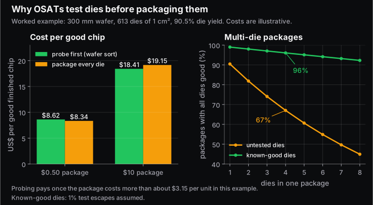
Step 4: multi-die packages make testing essential. In a 2.5D or chiplet package, one bad die scraps the whole assembly, including the interposer and the other good dies. If each die has a 90.48% chance of being good, a four-die package built from untested dies works only:
Probe-tested "known-good dies" (KGD) are not perfect either, because some faults escape the probe test. Assuming 1% escapes, the same package works of the time. That gap is why advanced-packaging lines spend heavily on wafer-level test. Real fabs also probe for reasons other than cost: wafer maps feed defect data back to the fab, and test results sort dies into speed grades.
Which OSAT and ATMP plants has India approved, and where do they stand?
India has approved nine OSAT/ATMP units under the first phase of the Semicon India Programme. As of 17 November 2026, five are in commercial production: Micron, Kaynes and CG Semi in Sanand, CDIL in Mohali and Suchi in Surat. Tata's Jagiroad plant has reported pilot production. HCL-Foxconn, 3D Glass Solutions and ASIP are under construction.
| Unit and location | Approved, investment | What it packages | Approved capacity | Status on 17 Nov 2026 |
|---|---|---|---|---|
| Micron, Sanand (Gujarat) | Jun 2023, ₹22,516 cr | DRAM and NAND memory: wafers into BGA packages, plus modules and SSDs | Phased; phase 1 has 500,000 sq ft of planned cleanroom | Commercial production since 28 Feb 2026 |
| CG Semi (CG Power with Renesas and Stars Microelectronics), Sanand | 29 Feb 2024, ₹7,600 cr | Chips for consumer, industrial, automotive and power uses | 15 million chips a day | Chip testing from Aug 2025; commercial production since 4 Jul 2026 at 20 crore units a year |
| Tata Semiconductor Assembly and Test, Jagiroad, Morigaon (Assam) | 29 Feb 2024, ₹27,000 cr | Wire bond, flip chip and integrated system-in-package | 48 million chips a day | Pilot production reported by the Assam CM on 3 Oct 2026; inauguration expected Dec 2026 to Jan 2027 (reported) |
| Kaynes Semicon, Sanand | 2 Sep 2024, about ₹3,300 cr | Intelligent power modules, much of it for export to a US customer | 60 lakh (6 million) chips a day | Production since 31 Mar 2026 |
| India Chip (HCL-Foxconn JV), Jewar (Uttar Pradesh) | May 2025, about ₹3,700 cr | Display driver chips for phones, laptops, cars and PCs | 20,000 wafers or 36 million units a month | Groundbreaking Feb 2026 |
| 3D Glass Solutions, Bhubaneswar (Odisha) | 12 Aug 2025, ₹1,943 cr | Glass substrates, glass interposers, 3D heterogeneous integration modules | About 69,600 glass panels, 50 million units and 13,200 3DHI modules a year | FSA Feb 2026; groundbreaking Apr 2026 |
| CDIL, Mohali (Punjab), brownfield expansion | 12 Aug 2025, ₹117 cr | Discretes: MOSFETs, IGBTs, Schottky diodes, transistors in silicon and silicon carbide | 158.38 million units a year | Commercial line launched 17 Sep 2026 |
| ASIP Technologies with APACT, Visakhapatnam (Andhra Pradesh) | 12 Aug 2025, ₹468 cr | Chips for mobile phones, set-top boxes and cars; wire bond and flip-chip BGA first (reported) | 96 million units a year | Foundation stone 1 Aug 2026 (reported); FSA Oct 2026; SEZ notified 10 Nov 2026 (reported) |
| Suchi Semicon, Surat (Gujarat) | 5 May 2026, part of ₹3,936 cr for two units | Discrete semiconductors for power electronics, analog and industrial uses | 1,033.20 million chips a year | Commercial line launched 17 Sep 2026 |
Sources: PIB and PMO Cabinet releases, the PIB backgrounder and the ISM timeline. SiCSem (Odisha) and Crystal Matrix (Dholera) also have packaging lines, but inside integrated fabs, so they are not counted in the nine.
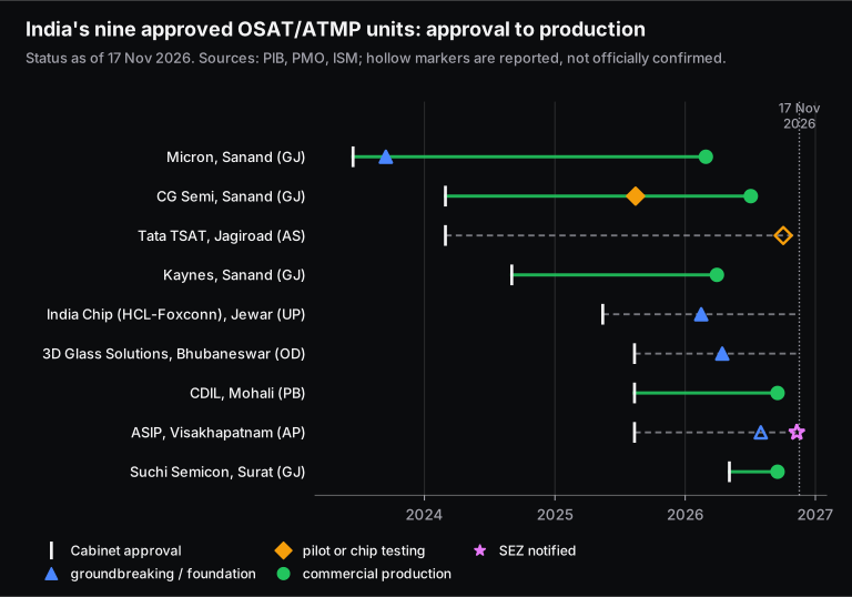
Three points stand out from the dates:
- The big greenfield plants took two to three years. Micron took 32 months from approval to commercial production and CG Semi 29. Kaynes, a smaller plant, took 18 months.
- Approval-to-production time is not build time. CDIL's was a brownfield expansion of an existing plant (13 months). Suchi's line started four months after approval, so some of its work clearly happened before approval.
- Start-up capacity is a fraction of the target. CG Semi's approval says 15 million chips a day, about 547 crore a year, and the Prime Minister cited a target of 500 crore units a year. At inauguration it ran at 20 crore a year, 4% of that target.
What jobs can mechanical, electrical and electronics graduates get in an OSAT?
OSAT plants hire mechanical, production and materials engineers for assembly processes, equipment, thermal-mechanical simulation and reliability, and electronics and electrical engineers for test, yield and package design. Diploma and ITI technicians run the lines.
| Role | Which steps | Best-fit degree | What you do and need |
|---|---|---|---|
| Assembly process engineer | Die attach, wire bond, flip-chip attach, moulding | Mechanical, production, metallurgy | Owns a process window (force, temperature, time); designed experiments, statistical process control (SPC), solders and epoxies |
| Equipment engineer | Grinders, dicing saws, bonders, moulding presses, test handlers | Mechanical, mechatronics, electrical | Keeps tools running and calibrated, cuts downtime; pneumatics, servo motion, PLCs, machine vision |
| Test engineer | Wafer sort, final test | Electronics, electrical | Writes test programs for automated test equipment, designs load boards, cuts test time; electronics, C or Python |
| Product and yield engineer | Sort and final-test data | Electronics | Reads wafer maps and bin data to find why yield dropped; statistics, scripting |
| Package and substrate design engineer | Before production | Electronics, electrical | Routes the substrate from bumps to balls, checks signal and power integrity; close to PCB design |
| Thermal-mechanical (CAE) engineer | Moulding, underfill, board-level reliability | Mechanical | Simulates warpage, thermal resistance and solder-joint fatigue with FEA, then matches models to measurements |
| Reliability and failure-analysis engineer | Qualification, returns | Mechanical, materials, electronics | Runs JEDEC stress tests, then X-rays and sections failed parts to find the root cause |
| Quality engineer | Whole line | Any engineering branch | Customer audits, corrective actions, FMEA and control plans, especially for automotive customers |
How to prepare, by branch:
- Mechanical and production: get good at heat transfer, materials (solders, polymers, fatigue) and FEA, since warpage and solder-joint life are FEA problems. Skill-Lync's Basics of FEA course and the FEA courses page are a starting point. Learn SPC and design of experiments, and read our FMEA guide, because every OSAT line runs on process FMEAs.
- Electronics and electrical: test engineering rewards solid digital and analog fundamentals and a scripting language. Our Basics of Digital Electronics course covers the logic that test patterns exercise. If you like layout, substrate design is a natural next step from PCB design.
- Embedded engineers: test programs, handler control and equipment software are embedded work. See the embedded systems courses.
- Where to look: the plants in commercial production are in Sanand, Surat and Mohali. Jagiroad is ramping up, and Jewar, Bhubaneswar and Visakhapatnam come next. For the wider list of chip employers, see top companies hiring embedded and VLSI engineers. For salary ranges, see our ISM 2.0 guide.
On scale, Micron said in 2023 that its project would create up to 5,000 direct jobs. Deccan Chronicle reported more than 1,000 direct jobs expected at ASIP.
What is the catch?
- Timelines slip. In June 2023 Micron expected phase 1 to start operating in late 2024. Commercial production began on 28 February 2026, about 14 months later.
- Ramp-up is slow. CG Semi started at 4% of its target volume. Tata's Jagiroad plant, the largest at 48 million chips a day, is still in pilot production.
- The wafers are imported. Indian OSATs package wafers made abroad until India's first fab, at Dholera, is commissioned. The government says that is scheduled for 2028 (PIB, 15 July 2026).
- Most capacity is legacy packaging. Memory, power modules, discretes and display drivers dominate the list. Glass interposers, 2.5D and 3D are planned, not running.
- The Vizag SEZ is reported, not yet confirmed. We are relying on India Briefing's reading of S.O. 6148(E) until the gazette copy appears on an official site.
Frequently asked questions
What is the full form of OSAT?
OSAT stands for outsourced semiconductor assembly and test. An OSAT company packages and tests chips for other companies. The related term ATMP, used in India's scheme documents, stands for assembly, testing, marking and packaging. It covers the same back-end steps, including plants owned by the chipmaker itself.
How many OSAT plants are there in India?
India has approved nine OSAT/ATMP units under the Semicon India Programme, in Gujarat, Assam, Uttar Pradesh, Odisha, Punjab and Andhra Pradesh. As of 17 November 2026, five were in commercial production: Micron, Kaynes and CG Semi in Sanand, CDIL in Mohali and Suchi Semicon in Surat. Tata's Assam plant has reported pilot production.
Is OSAT the same as a semiconductor fab?
No. A fab builds the transistors and wiring on a silicon wafer through hundreds of steps such as lithography, deposition and etch. An OSAT takes the finished wafer and tests, dices, packages and tests the chips again. Fabs cost far more and take longer to build, which is why India's first producing plants are all OSAT/ATMP units.
Can a mechanical engineer work in an OSAT?
Yes. OSATs hire mechanical engineers as assembly process engineers (die attach, wire bonding, moulding), equipment engineers, thermal-mechanical simulation engineers who model warpage and solder fatigue, reliability and failure-analysis engineers, and quality engineers. Heat transfer, materials, FEA and statistical process control are the most useful skills.
Sources and further reading
- India Briefing, India notifies semiconductor SEZ in Visakhapatnam, Andhra Pradesh (13 Nov 2026)
- Press Information Bureau, Semicon 2.0 web application portal launched; applications live for pillars 2, 3 and 4 (6 Nov 2026)
- India Semiconductor Mission, Semicon 2.0 scheme page, pillar 4 ATMP/OSAT and homepage timeline (read 17 Nov 2026)
- Press Information Bureau, Cabinet approves Semicon 2.0 (15 Jul 2026)
- Prime Minister's Office, Cabinet approves semiconductor units in Odisha, Punjab and Andhra Pradesh (12 Aug 2025)
- Press Information Bureau, India's Semiconductor Revolution, backgrounder with unit-wise investment and capacity (2025)
- Press Information Bureau, Cabinet approves three more semiconductor units (Tata fab, TSAT Assam, CG Power) (29 Feb 2024)
- Prime Minister's Office, Cabinet approves one more semiconductor unit (Kaynes) (2 Sep 2024); All India Radio, Cabinet approves Kaynes Semicon unit (2 Sep 2024)
- Press Information Bureau, Cabinet approves Crystal Matrix and Suchi Semicon (5 May 2026)
- Prime Minister's Office, PM inaugurates Micron's ATMP facility in Sanand (28 Feb 2026)
- Press Information Bureau, PM inaugurates the Kaynes Semicon plant at Sanand (31 Mar 2026)
- Press Information Bureau, PM inaugurates the CG Semi OSAT facility in Sanand (4 Jul 2026)
- Prime Minister's Office, PM inaugurates SEMICON India 2026 (Mohali and Surat lines) (17 Sep 2026)
- Micron, Micron announces new semiconductor assembly and test facility in India (22 Jun 2023)
- Autocar Professional, Tata Electronics begins semiconductor pilot in Assam (5 Oct 2026)
- Deccan Chronicle, Modi places stone for South India's first semiconductor facility in Vizag (1 Aug 2026)
- Amkor Technology, Flip chip, Copper pillar, Interconnect, 2.5D and 3D TSV, Wafer-level fan-out and Test services (read 17 Nov 2026)
- DISCO, Stealth Dicing process (read 17 Nov 2026)
- JEDEC, JESD22-A104, Temperature Cycling
- J. A. Cunningham, The use and evaluation of yield models in integrated circuit manufacturing, IEEE Transactions on Semiconductor Manufacturing 3(2), 60-71 (1990)
- J. L. Hennessy and D. A. Patterson, Computer Architecture: A Quantitative Approach, section on the cost of an integrated circuit (dies-per-wafer formula)