India Semiconductor Mission 2.0: 12 Chip Plants, Status and VLSI Jobs
ISM 2.0, approved as Semicon 2.0 with ₹1,27,500 crore, opened for applications on 6 November 2026. Here is where all 12 approved chip plants stand, what is confirmed and what is only reported about the Tata Dholera fab, which roles these plants and design centres hire for, and what VLSI engineers earn in India today.

In short
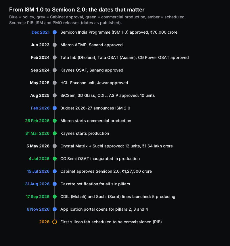
- The Union Cabinet approved Semicon 2.0, the second phase of the India Semiconductor Mission (the Budget called it ISM 2.0), on 15 July 2026 with an outlay of ₹1,27,500 crore. The scheme was notified on 31 August 2026, and applications for equipment, fabs and packaging opened on 6 November 2026.
- The first phase approved 12 chip units in six states worth about ₹1.64 lakh crore. Five are in commercial production: Micron, Kaynes and CG Semi in Sanand, Suchi Semicon in Surat and CDIL in Mohali. All five are assembly and test plants, not wafer fabs.
- India's first silicon fab, Tata Electronics' plant at Dholera, is under construction. The government says it is scheduled to be commissioned in 2028. Earlier reports of chips by December 2026 have not been confirmed.
- Chip design is still where most jobs and the best pay are. On AmbitionBox (November 2026), the average range for VLSI design engineers at semiconductor companies is ₹22.9-27.8 lakh, against ₹9.4-11.9 lakh for the same title at IT services firms.
India Semiconductor Mission 2.0 is the government's ₹1,27,500 crore programme to move India from a few chip packaging plants to a complete semiconductor industry: chip design and Indian IP, equipment and materials, more fabs, advanced packaging, research and talent. It builds on a first phase that approved 12 manufacturing units, of which five were shipping chips by October 2026.
This guide separates what is officially confirmed from what has only been reported. It covers what ISM 2.0 actually funds, where each of the 12 plants stands as of 14 November 2026, which jobs these plants and design centres hire for, and what VLSI and semiconductor roles pay in India today, with the source and date for every number.
What is ISM 2.0, and what exactly did the Cabinet approve?
The Union Budget 2026-27 announced "India Semiconductor Mission 2.0" for equipment and materials, full-stack chip design, Indian IP and stronger supply chains (MeitY in Rajya Sabha, 13 March 2026). The Union Cabinet approved it on 15 July 2026 under the official name Semicon 2.0, with a total outlay of ₹1,27,500 crore (PIB, 15 July 2026). ISM 2.0 and Semicon 2.0 are the same programme. At SEMICON India on 17 September 2026 the Prime Minister described it as a 13.5 billion dollar second phase (PMO, 17 September 2026).
For scale, the first phase, the Semicon India Programme notified in December 2021, had ₹76,000 crore (PIB backgrounder, 17 September 2026). The first phase concentrated on fabs and packaging plants. The second adds design, machines and materials, research and talent, so the support runs from raw materials to finished chips.
The scheme runs through six pillars and 10 categories. Projects can be supported for up to six years, the application window stays open for three years, and a mid-term review is due after three years. The India Semiconductor Mission (ISM) is the nodal agency and may run the design categories with help from C-DAC (PIB, 31 August 2026). The fiscal support published on the ISM scheme page is:
| Pillar | What it funds | Support published by ISM |
|---|---|---|
| 1. Design | Chips, SoCs and IP blocks for strategic needs (competitive bidding), commercial chip design, and a deployment-linked incentive | Seed funding up to ₹15 crore per commercial application; 9% of net sales for 5 years for deployed chips and IP |
| 2. Machines and materials | Semiconductor equipment, materials, chemicals and gases | 30% of capital expenditure |
| 3. Fabs | Silicon wafer fabs; compound semiconductor, photonics, sensor (including MEMS) and discrete fabs; display fabs | 40% of eligible capex for silicon fabs; 35% for the other two categories |
| 4. ATMP/OSAT | Assembly, test, marking and packaging plants | 35% for advanced packaging; 25% for legacy packaging |
| 5. Research and development | R&D on advanced semiconductor technologies | Category notified; rate not shown on the overview page |
| 6. Talent development | Design tools and multi-project wafer runs for colleges; training labs for shop-floor and fab staff | Up to 75% of project cost, with state incentive |
Two terms in that table need a plain-language explanation. Pari-passu support, which ISM uses for the fab pillar, means the government pays its share in step with what the company actually spends, not as an upfront grant. Capex is the money spent on land, buildings and tools. So if a silicon fab had ₹10,000 crore of eligible capex, central support could reach ₹4,000 crore (40%), released over the life of the project as the company itself spends. Source for the rates: ISM, Semicon 2.0 scheme page (read 14 November 2026).
The latest step came on 6 November 2026, when the Semicon 2.0 application portal opened for pillars 2, 3 and 4 (PIB, 6 November 2026). Companies can now apply. No project has yet been approved under Semicon 2.0 itself.
Which chip plants has India approved, and which are actually producing?
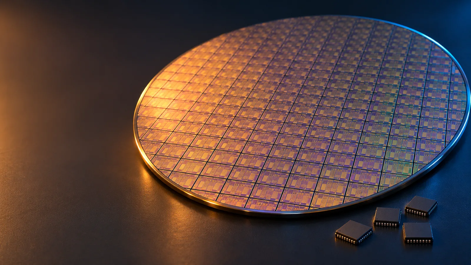
Two kinds of plant matter here. A fab (fabrication plant) builds transistors on a silicon wafer through hundreds of steps such as deposition, lithography and etching. An ATMP or OSAT plant (assembly, test, marking and packaging; outsourced semiconductor assembly and test) takes finished wafers, cuts out each chip, puts it in a protective package, and tests it. Think of the fab as the kitchen and the OSAT as the packing and quality-check line. Both are factories, but fabs cost far more and take longer to build.
Under the first phase, the Cabinet approved 12 units: one silicon fab, one silicon carbide fab, one gallium nitride micro-LED display fab and nine ATMP/OSAT units in Gujarat, Assam, Uttar Pradesh, Odisha, Punjab and Andhra Pradesh, with a combined investment of about ₹1.64 lakh crore (PIB, 17 September 2026). By October 2026, five had started commercial production (PIB, 6 November 2026).
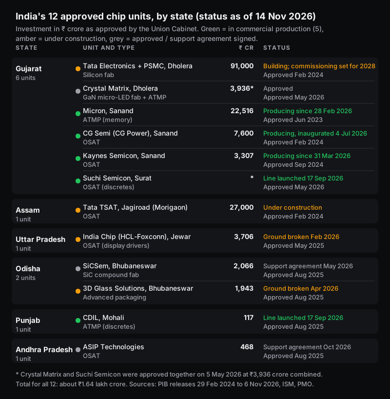
The five producing plants, in the order they started:
- Micron, Sanand (Gujarat). Memory assembly and test. Commercial production began on 28 February 2026, when the Prime Minister inaugurated the plant. The plant produces DRAM and NAND memory products (PMO, 28 February 2026).
- Kaynes Semicon, Sanand. Production started on 31 March 2026. The plant makes intelligent power modules, with a large share booked for export to a US customer (PIB, 31 March 2026).
- CG Semi, Sanand. An OSAT built with Renesas (Japan) and Stars Microelectronics (Thailand). It was inaugurated on 4 July 2026 at a capacity of 20 crore units a year, with a stated target of 500 crore units a year (PIB, 4 July 2026).
- CDIL, Mohali (Punjab) and 5. Suchi Semicon, Surat (Gujarat). Both make discrete semiconductors; CDIL's range includes MOSFETs, IGBTs and Schottky diodes. Their commercial lines were launched at SEMICON India on 17 September 2026 (PMO, 17 September 2026).
Note what this list does not include: no wafer fab. Every unit producing in India today is a back-end plant.
Confirmed vs reported: where the Tata fab and the other projects stand
Search results for "semiconductor fab India" mix government statements, company statements and property-site guesses. Here is what each kind of source actually says.
Confirmed by government releases
- Tata Electronics fab, Dholera: approved on 29 February 2024 with Powerchip Semiconductor Manufacturing Corp (PSMC) of Taiwan as technology partner, at ₹91,000 crore. It is planned for 50,000 wafers a month on 28 nm and other mature nodes, for compute, automotive and power-management chips (PIB, 29 February 2024; PIB backgrounder, 2025). In the Semicon 2.0 approval, the government said the first fab is "scheduled to be commissioned in 2028" (PIB, 15 July 2026).
- Tata Semiconductor Assembly and Test (TSAT), Jagiroad, Morigaon district, Assam: ₹27,000 crore, designed for 48 million chips a day. It is not among the five units the government counts as producing.
- India Chip (HCL-Foxconn), Jewar, Uttar Pradesh: display driver chips, approved in May 2025. The ISM timeline records its groundbreaking in February 2026 (ISM).
- Odisha and Andhra Pradesh: 3D Glass Solutions (glass substrates and advanced packaging) broke ground in Bhubaneswar in April 2026. SiCSem (silicon carbide power devices) signed its financial support agreement in May 2026, and ASIP Technologies signed in October 2026 (ISM timeline).
- Crystal Matrix, Dholera: approved on 5 May 2026 together with Suchi Semicon, at ₹3,936 crore for the pair. It will be India's first commercial mini/micro-LED display facility based on gallium nitride, planned at 72,000 square metres of display panels a year (PIB, 5 May 2026).
Reported or stated by companies, not confirmed by government
- At SEMICON India 2026, Tata Electronics CEO Randhir Thakur said construction at both Dholera and Jagiroad is on track. Tata also signed an agreement with Nexperia to prepare Dholera for Nexperia's MOSFETs and to assemble and test its discrete parts at Jagiroad, but neither company gave volumes or dates (EE Times, September 2026).
- Minister Ashwini Vaishnaw said an unnamed fab scheduled to start production in 2028 has already booked a large share of its capacity (same EE Times report).
- Several property and aggregator websites still say the Dholera fab will begin trial production in December 2026. We found no government or Tata statement that confirms this, and the government's own date is 2028. Treat any December 2026 claim as unverified.
Where the official numbers disagree
Talent figures vary between releases. The Cabinet note of 15 July 2026 said about 68,000 students had been trained in 315 universities. On 31 August 2026 the minister said the 85,000-engineer target had been reached. The Prime Minister's speech on 17 September and the PIB release of 6 November both put the number at 70,000, with 332 institutions given chip design tools under the Chips to Startup (C2S) programme. We use the latest figure, 70,000, and the trend matters more than the exact count.
How many jobs will India's semiconductor plants create?
The government's own job estimates, approval by approval:
| Approval | Units | Jobs stated in the approval |
|---|---|---|
| 29 Feb 2024 | Tata fab, Tata Assam OSAT, CG Power OSAT | 20,000 direct and about 60,000 indirect |
| 12 Aug 2025 | SiCSem, 3D Glass, CDIL, ASIP | 2,034 skilled professionals |
| 5 May 2026 | Crystal Matrix, Suchi Semicon | 2,230 skilled professionals |
| 31 Aug 2026 (ecosystem view) | Whole semiconductor ecosystem | 50,000-60,000 direct jobs expected |
Sources: PIB 29 Feb 2024, PMO 12 Aug 2025, PIB 5 May 2026, PIB 31 Aug 2026.
The plants are only one part of the picture. Government releases citing industry estimates say India hosts about 7% of the world's semiconductor global capability centres and employs nearly 20% of the global chip design workforce (PIB, 13 March 2026). Those design centres in Bengaluru, Hyderabad and Noida employ far more engineers than the new factories will for several years.
The factories also hire a different mix of people. A large share of plant jobs go to technicians and operators, not only graduate engineers. At the CG Semi inauguration, the Prime Minister spoke about young women from tribal communities with ITI training who were sent to Malaysia for advanced training before joining the Sanand line (PIB, 4 July 2026).
Which roles do semiconductor companies in India hire for?
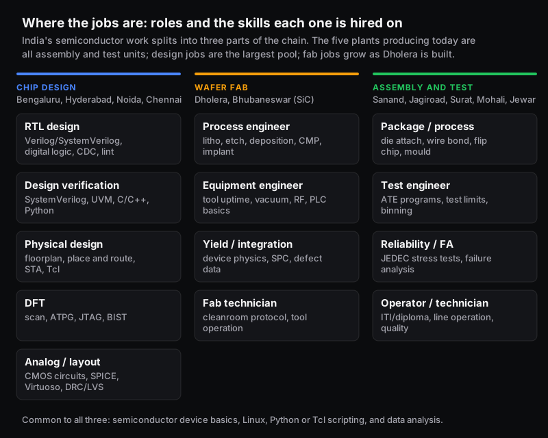
Semiconductor work in India falls into three groups, and each one hires on different skills and in different cities.
Chip design (VLSI)
VLSI (very large scale integration) is the design of chips with millions to billions of transistors. A digital chip passes through a chain of specialists:
- RTL design: describes the chip's logic in a hardware description language such as Verilog or SystemVerilog. RTL (register transfer level) is the code that says what happens on every clock tick.
- Design verification (DV): proves the RTL does what the specification says before anything is built, usually with SystemVerilog and the UVM methodology.
- Physical design (PD): turns the verified logic into a physical layout. That means placing millions of cells and routing the wires between them, then closing timing with static timing analysis (STA), which checks every signal arrives within its clock deadline.
- DFT (design for test): adds the scan chains and test logic that let a factory tester check every chip quickly. This is the link between design teams and the OSAT plants above.
- Analog design and layout: power management, data converters and RF circuits, drawn transistor by transistor.
Wafer fab
Process engineers own one step of manufacturing, such as lithography, etch, deposition, chemical-mechanical polishing (CMP) or ion implantation. Equipment engineers keep the tools running, and yield engineers work out from defect data why some chips on a wafer fail. These jobs suit electronics, electrical, chemical, mechanical and materials graduates. Fab hiring will build up as Dholera nears its scheduled 2028 commissioning.
Assembly and test (OSAT)
Package and process engineers run die attach, wire bonding, flip-chip and moulding lines. Test engineers write programs for automated test equipment (ATE) and set the pass and fail limits. Reliability engineers stress parts to JEDEC standards (the industry's reliability test standards) and analyse failures. Operators and technicians, many with ITI or diploma qualifications, run the lines. This is where hiring is happening right now, in Sanand, Surat and Mohali.
VLSI engineer salary in India: what the November 2026 data says
The table below uses AmbitionBox, where employees report their own pay. For each title AmbitionBox shows a "typical" average range for a given experience band and, where the sample is large enough, a range for each band. These are ranges of the average, not the lowest and highest salaries, so many individual offers fall outside them. All figures are in ₹ lakh a year and were read on 14 November 2026.
| Role (AmbitionBox title) | Typical average range | By experience | Salaries in sample |
|---|---|---|---|
| VLSI Design Engineer | 18.1-21 (0-5 yrs) | Not shown by band | 458 |
| Analog Design Engineer | 17.7-19.6 (0-5 yrs) | Not shown by band | 868 |
| DFT Engineer | 14.7-16.3 (1-6 yrs) | 1-3 yrs: 10-11.5; 3-6 yrs: 15.6-17.6; 6-9 yrs: 24.6-32.5 | 634 |
| Verification Engineer | 13.3-14.7 (0-5 yrs) | Not shown by band | 2,100 |
| Analog Layout Engineer | 10.3-11.4 (1-7 yrs) | 1-3 yrs: 6-6.6; 3-6 yrs: 9.5-10.7; 6-9 yrs: 23.3-29.3 | 835 |
| RTL Design Engineer | 10.4-11.4 (0-6 yrs) | 0-1 yr: 6.5-7.2 (estimate); 1-3 yrs: 7.6-8.4; 3-6 yrs: 10.8-11.9 | 1,000 |
| Physical Design Engineer | 9.5-10.5 (1-4 yrs) | 1-3 yrs: 6.8-7.6; 3-6 yrs: 10.9-12 | 2,800 |
Two patterns stand out. First, pay climbs steeply after about six years: by midpoint, the DFT average rises about 70% and the analog layout average about 160% from the 3-6 year band to the 6-9 year band (those senior bands have only 29 and 36 salaries, so treat them as indicative). Second, and more important for anyone choosing an employer, the same job title pays very differently depending on who you work for.
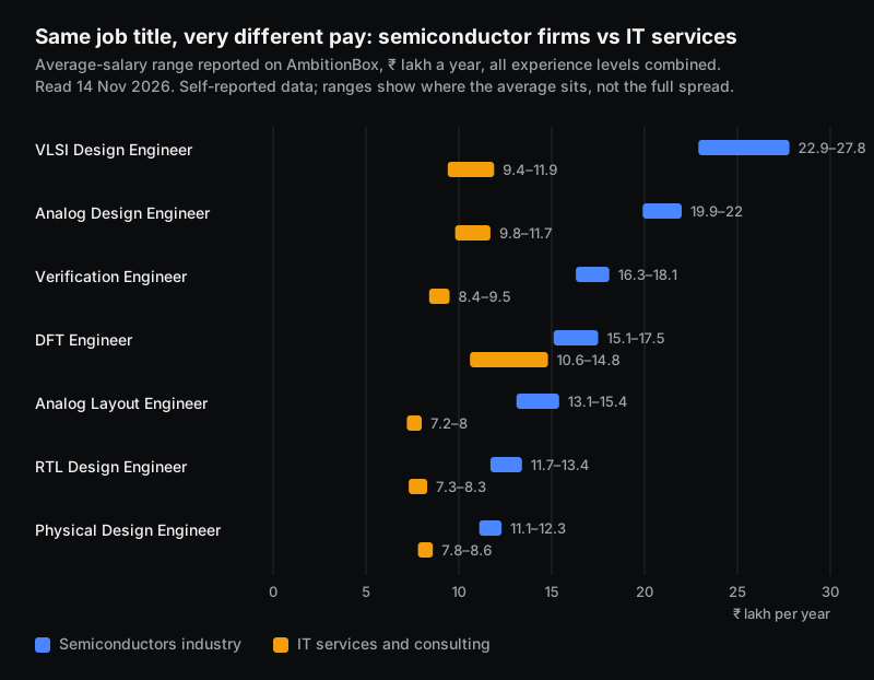
A worked comparison makes the gap concrete. Take the midpoints for a verification engineer: ₹17.2 lakh at semiconductor firms ((16.3 + 18.1) / 2) and ₹8.95 lakh at IT services firms ((8.4 + 9.5) / 2). That is a ratio of about 1.9. Some of the gap may come from differences in experience mix, but company-level numbers show the same pattern. For the VLSI Design Engineer title, AmbitionBox lists average ranges of ₹34.5-48.4 lakh at Texas Instruments, ₹30.4-43 lakh at Nvidia, ₹23.4-35.1 lakh at Qualcomm and ₹20.5-27.9 lakh at Intel, against ₹5-7.4 lakh at Wipro. On these numbers, moving from a services firm to a semiconductor product company can be the biggest pay jump available to a VLSI engineer, bigger than a change of city.
City matters less than employer. For VLSI design engineers, the Bengaluru average range is ₹18.9-23.7 lakh and Hyderabad is ₹14.5-19.6 lakh. Physical design engineers in Ahmedabad, the city nearest the Sanand cluster, report ₹6.4-8.3 lakh, below Bengaluru's ₹9.7-10.7 lakh, but that sample has only 44 salaries.
Fab and OSAT roles have much less public pay data because most plants are new. Micron's process engineers in India with 0-2 years' experience report an average range of ₹9.3-12.1 lakh, but that is only 11 salaries and AmbitionBox rates its confidence as medium. Process engineers at GlobalFoundries (₹11.3-15 lakh) and Applied Materials (₹13.8-19.6 lakh) in India report higher averages, though those are small samples too. Treat these as early indicators, not benchmarks.
Pay is rising. AmbitionBox shows average physical design salaries up 19% and RTL design salaries up 18% over the last two years. For a wider view of salaries across VLSI roles, see our VLSI engineer career and salary guide.
What should students and engineers learn to get these jobs?
The right path depends on where you start:
- ECE and EEE students aiming at design: get digital logic, CMOS basics and Verilog solid first, then pick one track: verification (SystemVerilog, UVM), physical design (STA, place and route, Tcl) or DFT (scan, ATPG). Linux and Python or Tcl scripting are expected in every track. Skill-Lync's Basics of Digital Electronics course covers the digital design fundamentals that every VLSI track builds on.
- Use the C2S programme if your college is in it. The government says 332 institutions have been given industry EDA tools, and 211 chips had been taped out by 75 institutions by April 2026 (PIB, 13 August 2026). A taped-out student chip on your CV is strong evidence of skill.
- Mechanical, chemical and materials graduates have a real route into fabs and OSATs as process, equipment and reliability engineers. Learn semiconductor device and process basics, statistical process control and cleanroom practice, and watch the hiring pages of the units in Dholera, Sanand, Jagiroad and Bhubaneswar.
- Embedded engineers fit naturally into post-silicon validation, chip bring-up and applications roles, where you write the firmware that tests and uses a new chip. Our Pre-Graduate Program in Embedded Systems covers C, microcontrollers and the hardware-software interface those roles need. For a map of companies hiring in both fields, see top companies hiring embedded and VLSI engineers.
- Diploma and ITI holders: operator and technician posts in OSAT plants are the fastest-growing entry point right now. CG Semi, for example, sent ITI-qualified hires to Malaysia for training.
What ISM 2.0 does not guarantee
The momentum is real, but a few limits are worth keeping in mind before you plan a career around it.
Every producing unit is a back-end plant. Packaging and test matter, but wafer fabrication, the step where transistors are actually made, does not start in India until the Dholera fab is commissioned, which the government schedules for 2028. Until then, Indian plants package wafers made elsewhere.
The nodes are mature. The government describes India's starting point as 28 nm to 110 nm. Those nodes are needed for cars, power electronics and industrial chips, but leading-edge processor manufacturing stays abroad. India's leading-edge work is in design, where Indian teams already work on 2 nm chips for global companies (PIB, 13 March 2026).
Investment announcements are commitments, not money spent. Semicon 2.0 support is paid in step with company spending over up to six years. At SEMICON India, the minister said the roughly ₹1 lakh crore of investment commitments announced there would materialise over two to three years as companies secure board approvals (EE Times).
The salary data is self-reported. AmbitionBox ranges show where averages sit, and small samples (fab roles, smaller cities) can move a lot. Use them to compare options, not as a promise of what an offer will be.
Design jobs will stay concentrated in Bengaluru, Hyderabad and Noida, while new manufacturing jobs are in Dholera, Sanand, Surat, Jagiroad, Jewar, Mohali and Bhubaneswar. Where you are willing to live will shape which of these jobs is realistic for you.
Frequently asked questions
Is ISM 2.0 the same as Semicon 2.0?
Yes. The Union Budget 2026-27 announced it as India Semiconductor Mission 2.0. The Cabinet approved it on 15 July 2026 under the name Semicon 2.0, with an outlay of ₹1,27,500 crore. The India Semiconductor Mission is the agency that runs it.
Has India started making chips?
India has started assembling, packaging and testing chips commercially. Five plants were in commercial production by October 2026: Micron, Kaynes and CG Semi in Sanand, Suchi Semicon in Surat and CDIL in Mohali. India does not yet have a commercial wafer fab. The first, Tata Electronics' plant at Dholera, is scheduled to be commissioned in 2028.
When will the Tata Dholera fab start production?
The government's latest stated date is 2028, given in the Semicon 2.0 approval on 15 July 2026. Tata's CEO said in September 2026 that construction is on track. Reports of trial production in December 2026 have not been confirmed by the government or Tata.
What is the salary of a VLSI engineer in India?
On AmbitionBox in November 2026, typical average ranges were ₹18.1-21 lakh a year for VLSI design engineers with 0-5 years' experience, ₹13.3-14.7 lakh for verification engineers and ₹9.5-10.5 lakh for physical design engineers with 1-4 years. Freshers in RTL design average around ₹6.5-7.2 lakh (an AmbitionBox estimate). By midpoint, averages at semiconductor companies are about 1.3 to 2.4 times those at IT services firms for the same title.
Can mechanical engineers get semiconductor jobs?
Yes, mostly on the manufacturing side. Fabs and OSAT plants hire mechanical, chemical and materials engineers as process, equipment, facilities and reliability engineers. Chip design roles normally need electronics fundamentals and hardware description languages.
Which Indian states have semiconductor plants?
The 12 approved units are in six states: Gujarat (6), Odisha (2), Assam, Uttar Pradesh, Punjab and Andhra Pradesh (1 each). Gujarat's Sanand and Dholera are the largest clusters.
Sources and further reading
- Press Information Bureau, Cabinet approves Semicon 2.0 (15 July 2026)
- Press Information Bureau, Union Minister Ashwini Vaishnaw addressed media on Semicon 2.0; notifications for all 6 pillars issued (31 August 2026)
- Press Information Bureau, India Building Semiconductor Future (backgrounder) (17 September 2026)
- Press Information Bureau, Semicon 2.0 web application portal launched (6 November 2026)
- Press Information Bureau, Cabinet approves two more semiconductor units (Crystal Matrix, Suchi Semicon) (5 May 2026)
- Press Information Bureau, PM inaugurates CG Semi OSAT facility in Sanand (4 July 2026)
- Press Information Bureau, PM inaugurates the Kaynes Semicon plant at Sanand (31 March 2026)
- Press Information Bureau, India has emerged as a global hub for semiconductor design and R&D (13 March 2026)
- Press Information Bureau, Semiconductor and AI Revolution (backgrounder) (13 August 2026)
- Press Information Bureau, Cabinet approves three more semiconductor units (29 February 2024)
- Press Information Bureau, India's Semiconductor Revolution (backgrounder with unit-wise investment) (2025)
- Prime Minister's Office, PM inaugurates Micron's ATMP facility in Sanand (28 February 2026)
- Prime Minister's Office, PM inaugurates SEMICON India 2026 (17 September 2026)
- Prime Minister's Office, Cabinet approves semiconductor units in Odisha, Punjab and Andhra Pradesh (12 August 2025)
- India Semiconductor Mission, Semicon 2.0 scheme details and timeline of milestones (read 14 November 2026)
- EE Times, SEMICON India 2026: India starts packaging chips as ecosystem takes shape (September 2026)
- AmbitionBox salary pages, read 14 November 2026: VLSI Design Engineer, Verification Engineer, Physical Design Engineer, DFT Engineer, RTL Design Engineer, Analog Design Engineer, Analog Layout Engineer, Micron Technology Process Engineer