GlobalFoundries Invests USD 10 Mn in Cyient Semiconductors: What It Means
On 19 November 2026 Cyient Semiconductors approved a USD 10 million strategic equity investment from GlobalFoundries at a USD 490 million pre-money valuation (USD 510 million combined post-money). Here is what is confirmed and what is only reported, how the fabless-foundry model works, a worked cost-per-chip example, and the VLSI roles it points to for Indian ECE students.

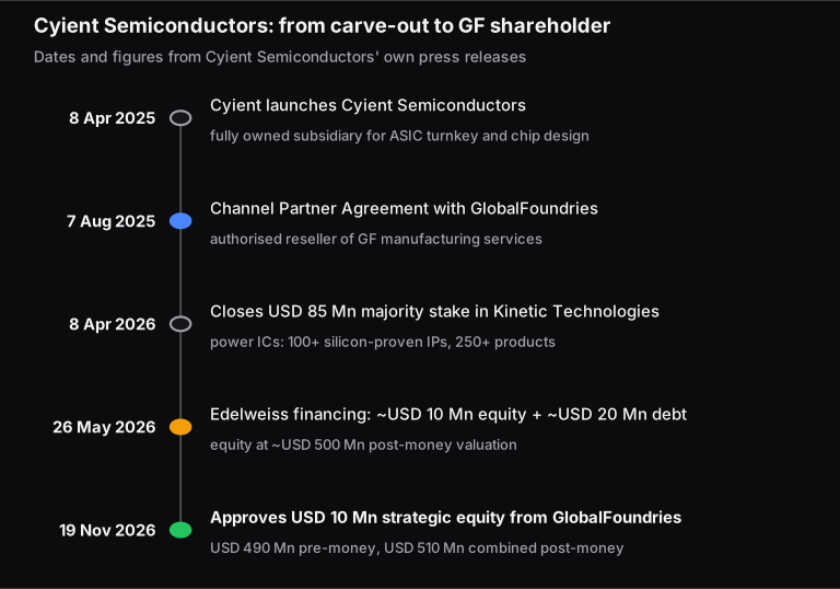
On 19 November 2026, Cyient Semiconductors, the chip design company carved out of engineering firm Cyient, said it had approved a USD 10 million strategic equity investment from GlobalFoundries (GF), the contract chipmaker headquartered in Malta, New York. The price matches Cyient Semiconductors' Edelweiss round from May: a USD 490 million pre-money valuation. With both investments counted, the combined post-money valuation is USD 510 million. GF was already the company's foundry partner. Now it will also be a shareholder.
This post covers what the company confirmed and what is only reported. It then explains the fabless-foundry model behind the deal and works through the numbers a chip design house lives by. It ends with the VLSI roles that companies like this hire for in India. For India's chip plants and the ISM 2.0 scheme, see our India Semiconductor Mission 2.0 guide. For what happens after the wafer leaves the fab, see semiconductor OSAT in India.
Key facts at a glance
- 19 November 2026: Cyient Semiconductors approved a USD 10 million strategic equity investment by GlobalFoundries. Source: Cyient Semiconductors press release, Hyderabad, 19 Nov 2026.
- Valuation: USD 490 million pre-money, the same as the Edelweiss-led round, and a USD 510 million combined post-money equity valuation (same release).
- Purpose, as stated: expand turnkey custom ASIC work, speed up custom silicon development, and strengthen "long-term wafer supply assurance" (same release).
- Reported, not in the release: the investor is GlobalFoundries U.S. Inc., subscribing to compulsorily convertible cumulative preference shares (CCPS). HDFC Sky News and Indian Startup News report this, citing parent Cyient Ltd's stock-exchange filing, 19-20 Nov 2026.
- Background: Cyient Semiconductors became an authorised GF channel partner (a reseller of GF wafer manufacturing) on 7 August 2025. In May 2026 it raised about USD 10 million equity plus USD 20 million debt from Edelweiss (company releases).
Courses: the digital design basics behind RTL and verification jobs are covered in Skill-Lync's Basics of Digital Electronics course. The free VLSI Design interactive book goes from the MOS transistor to the ASIC flow.
What did Cyient Semiconductors announce on 19 November 2026?
Cyient Semiconductors said it approved a USD 10 million strategic equity investment by GlobalFoundries. It will be done at the same USD 490 million pre-money valuation as its recent Edelweiss-led round, for a combined post-money equity valuation of USD 510 million. The company says the money will grow its custom ASIC business and secure long-term wafer supply.
Here is what is confirmed, what is reported and what nobody has said yet:
| Detail | Status | Where it comes from |
|---|---|---|
| USD 10 million strategic equity investment by GF, approved | Confirmed | Cyient Semiconductors release, 19 Nov 2026 |
| USD 490 million pre-money, USD 510 million combined post-money | Confirmed | Same release |
| Uses: turnkey custom ASIC, custom silicon development, wafer supply assurance | Confirmed | Same release |
| Instrument: compulsorily convertible cumulative preference shares; investor entity GlobalFoundries U.S. Inc. | Reported | HDFC Sky News (19 Nov) and Indian Startup News (20 Nov), citing Cyient Ltd's exchange filing. We could not open the filing itself. |
| Stake of about 2% | Our arithmetic | USD 10 million ÷ USD 510 million; no stake is stated in the release |
| A statement from GF | Not published | GF's newsroom had no release on the deal when we checked on 21 Nov 2026 |
| Closing date, board seat, capacity commitments | Not stated | Neither the release nor the reports give them |
Suman Narayan, CEO of Cyient Semiconductors, said in the release that having a leading ecosystem partner as a strategic investor "validates our technology and business model" and "accelerates our access to advanced manufacturing capabilities".
How do the valuation numbers add up?
The two rounds were priced on the same base, so the arithmetic is simple. The company was valued at USD 490 million before new money. Edelweiss's roughly USD 10 million took it to about USD 500 million, the figure Cyient Semiconductors announced on 26 May 2026. GF's USD 10 million on the same pre-money base takes the combined figure to USD 510 million:
If the preference shares convert at that price, each investor would hold about . Treat that as an estimate: the company has not published a shareholding, and the conversion terms are not public. The point is that GF bought a small minority stake. It is a strategic tie-up, not a takeover.
Who is Cyient Semiconductors?
Cyient Semiconductors is a fabless chip company from Hyderabad. It designs custom chips (ASICs) and power ICs, and has them made by foundries such as GF. Cyient Ltd, the engineering services firm, launched it as a fully owned subsidiary in April 2025. It brought along Cyient's 25+ years of ASIC turnkey and chip design work, with teams in India, the US, Germany, Belgium, the Netherlands and Taiwan.
"Turnkey ASIC" means the company takes a customer's requirement and delivers finished, tested chips. It handles the architecture, design, foundry, packaging, test and supply chain. Its own description covers analog, mixed-signal, RF and digital silicon for data centres, industrial automation, communications, automotive and healthcare. It works under both turnkey and design-service models.
Since the carve-out it has moved towards owning products as well as delivering services:
- Kinetic Technologies (closed 8 April 2026): a USD 85 million majority stake in a power semiconductor company with over 100 silicon-proven IPs and more than 250 high-volume custom and standard products.
- Partnerships: GF (wafer access), Navitas (what the company calls India's first GaN power IC family) and MIPS (RISC-V based power solutions).
- Government work: the May 2026 release says it secured the modernisation programme for SCL, the government's Semi-Conductor Laboratory at Mohali.
The May 2026 Edelweiss money was earmarked for product R&D, in-house validation and test facilities in India, and working capital.
What does GlobalFoundries make?
GlobalFoundries is a contract chip manufacturer, or foundry: it makes wafers to other companies' designs. Its processes target power, radio, low-power edge and optical chips. The most advanced logic process in its current line-up is a 12 nm-class FinFET, and GF's roadmap adds an FD-SOI platform it expects to deliver 7 nm-class digital performance. Its fabs are in Malta and Burlington (US), Dresden (Germany), Singapore and Guangzhou (China). It has none in India.
The processes GF lists, and what each is used for:
| GF platform | What it is | Typical chips |
|---|---|---|
| FDX (FD-SOI) | Planar transistors on a thin insulating layer. GF says it has been in volume production since 2019, with 700+ qualified IPs and adaptive body biasing. | Low-power edge AI, IoT, automotive radar, mmWave |
| FinFET (12 nm class) | 3D fin transistors. GF says it has shipped over 3 million wafers since 2015, with high-volume production at Malta, New York. | Higher-performance SoCs, AI at the edge |
| BCD, BCDLite, Power GaN | Bipolar, CMOS and DMOS on one chip; gallium nitride for power switching | Power management ICs, motor drivers, converters |
| RF SOI, SiGe, RF GaN | Processes tuned for radio frequency | 5G front ends, satellite links, radar |
| Silicon photonics | Optical components on silicon | Data centre optical links |
Cyient Semiconductors' own GF page lists the same families. It says it offers PDK support, MPW (multi-project wafer) runs for prototypes, wafer-order coordination and optional assembly and test.
Why would a foundry invest in a chip design company?
A foundry earns money only when someone tapes out a design on its process and orders wafers. Design houses like Cyient Semiconductors decide which process their customers' chips use. Each design they place on GF's process can become years of wafer orders. A small stake ties GF more closely to a partner that already resells its manufacturing.
That is our reading of the logic. Neither company has stated a motive beyond the release's own wording. What the record shows:
- The partnership came first. In August 2025, Cyient Semiconductors became an authorised reseller of GF's manufacturing services. It offers fabrication access, design enablement, assembly and test to fabless companies. GF said then that the deal fitted its channel strategy to serve "high-potential but underrepresented customers".
- Switching is expensive. A chip is designed against one foundry's process design kit (PDK). Moving it to another process means redoing much of the physical design and paying for a new mask set. So the foundry chosen at the start usually makes the chip for its whole life.
- Cyient wants supply security. The release names "long-term wafer supply assurance and supply chain resilience" as an aim. A shareholder foundry is a stronger supply partner than a vendor.
What is the fabless-foundry model?
In the fabless-foundry model, one company designs the chip and a different company manufactures it. The fabless company owns the design and the customer. The foundry owns the fab and the process. A third company, the OSAT, usually packages and tests the chips. Splitting the work this way lets a design team build chips without spending billions on a fab.
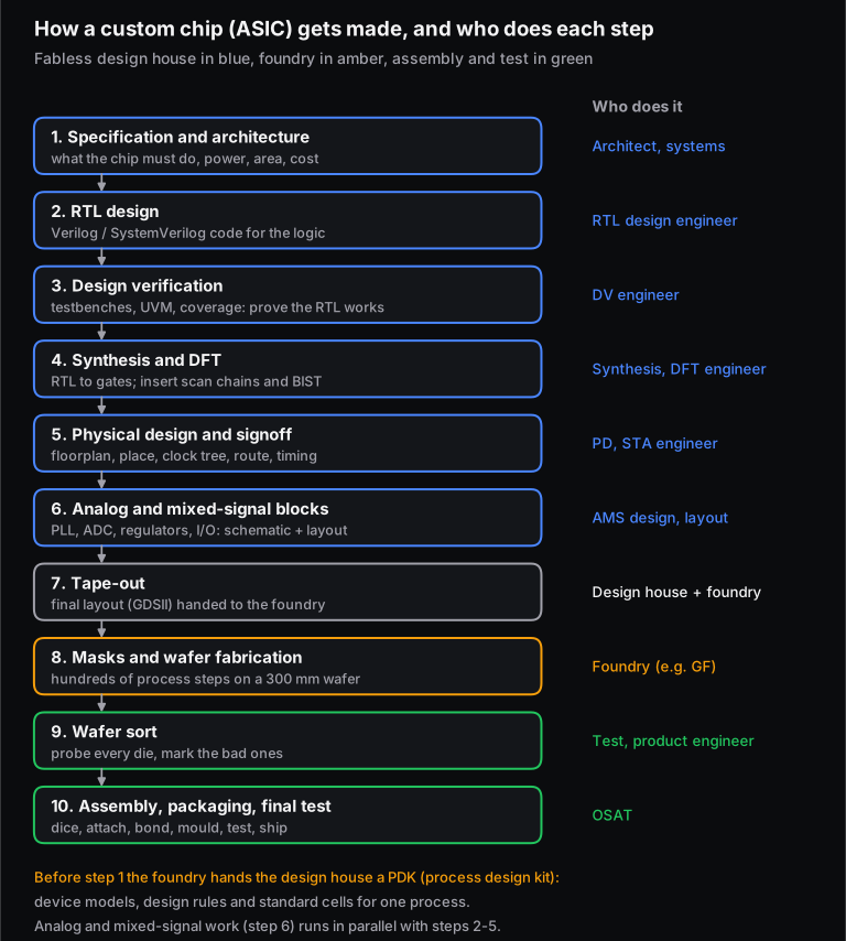
The handover between the two is a file. The foundry gives the designer a PDK: device models, design rules and standard-cell libraries for one process. The designer returns a finished layout, traditionally a GDSII file. That handover is the "tape-out". The foundry then makes the masks and processes the wafers. Cyient Semiconductors sits on the design side; GF on the manufacturing side. India's approved OSAT plants, covered in our OSAT guide, do the back end, and the machines inside fabs and OSATs are covered in our semiconductor equipment guide.
What are the steps from chip specification to a packaged chip?
A custom chip goes through specification, RTL design, verification, synthesis with test insertion, physical design and signoff, then tape-out. The foundry then makes masks and wafers, and an OSAT probes, packages and tests the dies. The first six steps happen at the design house. Each one is a separate job family.
Two points that textbook flowcharts often skip:
- Verification decides whether the first silicon works. A mask set is too expensive to throw away on a logic bug. So DV engineers write testbenches and coverage models that try to break the RTL before it is frozen, and the design is not taped out until coverage goals are met.
- DFT is planned before layout. Scan chains and built-in self-test (BIST) go in at synthesis, so the testers at wafer sort and final test can later detect manufacturing faults quickly. Our book chapter on testing, ATPG and scan design shows how.
For a step-by-step walk through the 13 stages of the digital flow, with a setup and hold timing example, read our VLSI design flow guide.
Worked example: what does one good chip cost a design house?
A design house pays per wafer, but it sells good chips. Two numbers decide its cost. The first is how many working dies come off each wafer, which depends on die area and the defect rate. The second is how many chips it sells to spread the one-time design and mask cost. Here is a scripted example with illustrative round numbers. These are not GF or Cyient prices.
Assumptions: a 300 mm wafer with a 3 mm unusable edge (usable diameter mm), wafer price USD 3,000, defect density per cm², and a one-time NRE (non-recurring engineering: masks and tape-out) of USD 1.5 million. We compare a 5 mm × 5 mm die ( mm², the size of a small power-management or mixed-signal ASIC) with a 10 mm × 10 mm die (100 mm²).
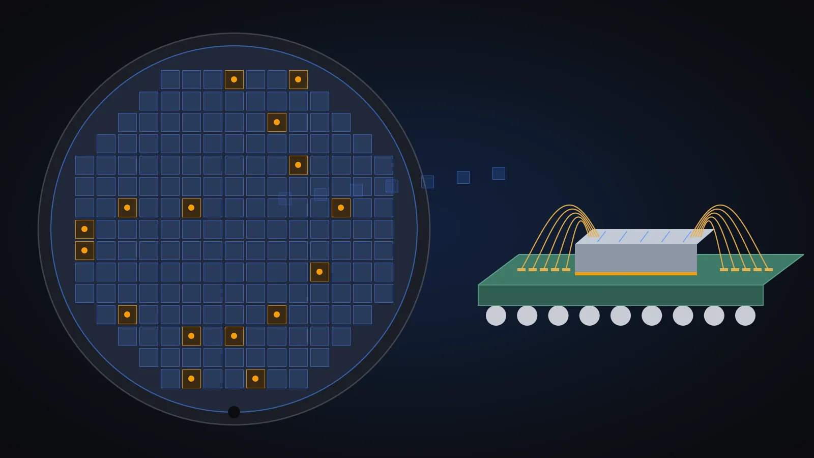
Step 1: gross dies per wafer. Divide the wafer area by the die area, then subtract the partial dies lost around the round edge:
For the 25 mm² die: , so 2,584 whole dies. For the 100 mm² die: , so 613 dies.
Step 2: how many are good? Our OSAT post used the simple Poisson model. Here we use Murphy's model, which allows for defect density varying across a wafer and is less pessimistic for larger dies:
With in cm², the small die has and , so 2,520 good dies. The large die has and , so 555 good dies.
Step 3: cost per good die. USD 3,000 ÷ 2,520 = USD 1.19 for the small die. USD 3,000 ÷ 555 = USD 5.41 for the large one. That is 4.54 times the cost for 4 times the area. Two effects stack up: the small die gets 4.22 times as many gross dies because less is lost at the wafer edge, and its yield is 1.077 times higher. This is why architects fight for every square millimetre.
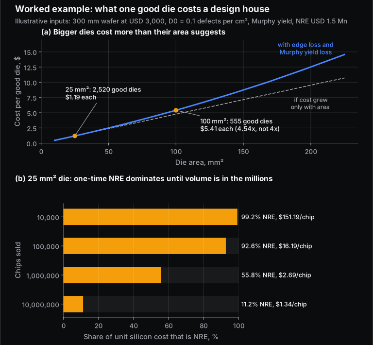
Step 4: spread the NRE. Unit silicon cost = cost per good die + NRE ÷ volume. For the small die:
| Chips sold | NRE per chip | Silicon cost per chip | NRE share |
|---|---|---|---|
| 10,000 | USD 150.00 | USD 151.19 | 99.2% |
| 100,000 | USD 15.00 | USD 16.19 | 92.6% |
| 1,000,000 | USD 1.50 | USD 2.69 | 55.8% |
| 10,000,000 | USD 0.15 | USD 1.34 | 11.2% |
NRE per chip equals the cost per good die at 1.26 million units. Below that, the one-time cost dominates. This is why low-volume customers start on shared MPW shuttles, which split one mask set across many designs. It is also why a turnkey ASIC house adds value by bringing many customers to a foundry.
Step 5: what it means for the foundry. One million good small dies need 397 wafers. One million large dies need 1,802. Every design a partner like Cyient Semiconductors brings to GF turns into wafer starts for as long as the chip sells.
The ASIC flow and yield chapter of our VLSI book has more practice problems on dies per wafer and yield.
What does this mean for VLSI and ECE students in India?
The deal does not create a fab in India. It strengthens a Hyderabad-based design company that does architecture, RTL, verification, DFT, physical design, analog design and test work. For electronics and electrical graduates, those design roles are the main openings at fabless and turnkey ASIC firms. Each needs a specific skill set.
| Role | What you do | What to learn first |
|---|---|---|
| RTL design engineer | Write synthesizable Verilog/SystemVerilog for blocks such as controllers, interfaces and datapaths | Digital logic, FSMs, timing basics, Verilog |
| Design verification (DV) | Build testbenches, write assertions and coverage, find bugs before tape-out | SystemVerilog, UVM, scripting (Python/Perl) |
| DFT engineer | Insert scan chains, run ATPG, plan memory BIST and boundary scan | Fault models, scan design, test basics |
| Physical design / STA | Floorplan, place, build the clock tree, route, close timing and power | CMOS, setup/hold, Tcl, Linux |
| Analog / mixed-signal | Design regulators, ADCs, PLLs and I/O in schematic and layout. This is central to power ICs like Kinetic's. | Analog circuits, MOSFET models, SPICE |
| Test and product engineering | Bring up silicon, write wafer-sort and final-test programs, analyse yield | Device physics, test equipment, data analysis |
A practical route for a final-year ECE student:
- Get digital logic airtight: combinational and sequential circuits, FSMs and timing. Our Basics of Digital Electronics course covers this ground.
- Write and simulate real RTL with a testbench. Free simulators are enough. The Verilog and RTL chapter of our VLSI book walks through a state machine.
- Pick a lane (DV, PD or analog) by your final semester and build one end-to-end project in it, such as a UART with a coverage-driven testbench.
- Learn Linux, Tcl and Python scripting. Every role above uses them daily.
For the companies that hire for these roles in India, see top companies hiring embedded and VLSI engineers. For pay data, see the VLSI salary section of our ISM 2.0 guide. If you are weighing embedded against VLSI, the embedded systems courses page shows where the two overlap.
What is the catch?
The deal is small and early. USD 10 million is a modest strategic stake, worth about 2% at the stated valuation. The company says it "approved" the investment, and trade reports describe a "proposed" subscription. No closing date has been given. GF had not published its own statement by 21 November 2026.
A few more limits are worth keeping in mind:
- No capacity numbers. "Wafer supply assurance" is an aim in the release. No volume or price commitment has been disclosed.
- A private valuation. USD 510 million is the price two strategic or financial investors agreed to pay for a small stake. It is not a market price, and minority rounds can carry terms that are not public.
- Design, not manufacturing. Chips designed in Hyderabad will still be made in GF's fabs in the US, Europe or Asia. The jobs this supports in India are mainly design and test jobs, not fab jobs.
- The filing details are second-hand here. We could not open Cyient Ltd's exchange filing. The instrument and investor entity above are as reported by two outlets.
Frequently asked questions
How much did GlobalFoundries invest in Cyient Semiconductors?
USD 10 million, as a strategic equity investment. Cyient Semiconductors announced it on 19 November 2026 at a USD 490 million pre-money valuation, the same as its May 2026 Edelweiss round. With both investments counted, the combined post-money equity valuation is USD 510 million.
What is Cyient Semiconductors' valuation?
Per the company's 19 November 2026 release, USD 510 million combined post-money, after USD 10 million each from Edelweiss and GlobalFoundries on a USD 490 million pre-money base. In May 2026 the company had stated about USD 500 million post-money (INR 4,600 crore) after the Edelweiss equity alone.
Is Cyient Semiconductors a fabless company?
Yes. It describes itself as a fabless semiconductor company. It designs chips and has them made by foundries such as GlobalFoundries, then coordinates packaging and test. It also offers turnkey ASIC services, delivering finished chips to a customer's specification, and design services.
What is the difference between a fabless company and a foundry?
A fabless company designs chips but owns no fab. A foundry owns the fab and manufactures wafers to other companies' designs. The handover is the tape-out: the designer sends the final layout drawn to the foundry's PDK rules, and the foundry makes the masks and wafers.
Does GlobalFoundries have a fab in India?
No. GF's manufacturing page lists fabs in Malta, New York; Burlington, Vermont; Dresden, Germany; Singapore; and Guangzhou, China. This investment is in an Indian design company, not in Indian manufacturing.
Which VLSI skills do chip design companies in India hire for?
Mostly RTL design (Verilog/SystemVerilog), design verification (SystemVerilog, UVM), DFT (scan, ATPG, BIST), physical design and static timing analysis (Tcl, Linux), analog and mixed-signal design (SPICE, layout), and test or product engineering. Strong digital logic fundamentals and scripting help in every one of them.
Sources and further reading
- Cyient Semiconductors Secures Strategic Investment from GlobalFoundries, Cyient Semiconductors press release, 19 Nov 2026 (primary source for the deal).
- Cyient Semiconductors Announces Strategic Financing with Edelweiss at ~USD 500 Mn Equity Valuation, Cyient Semiconductors, 26 May 2026.
- Cyient Semiconductors Enters Strategic Channel Partnership with GlobalFoundries, Cyient Semiconductors, 7 Aug 2025.
- Cyient Announces the Launch of Semiconductor Subsidiary, Cyient, 8 Apr 2025.
- Cyient Semiconductor Announces Successful Close of Majority Investment in Kinetic Technologies, Cyient Semiconductors, 8 Apr 2026.
- MIPS and Cyient Semiconductor collaborate to bring Custom RISC-V-based intelligent power solutions, Cyient Semiconductors, 12 Jun 2025.
- GlobalFoundries Wafer Access, Cyient Semiconductors (accessed 21 Nov 2026).
- FDX FD-SOI technology and FinFET, GlobalFoundries (accessed 21 Nov 2026).
- Manufacturing and Newsroom, GlobalFoundries (accessed 21 Nov 2026).
- Cyient Semiconductor Gets $10 Mn Investment; Shares Flat, HDFC Sky News, 19 Nov 2026 (reported instrument and investor entity).
- From foundry partner to shareholder: GlobalFoundries puts $10 million into Cyient Semiconductors, Indian Startup News, 20 Nov 2026.
- B. T. Murphy, Cost-size optima of monolithic integrated circuits, Proceedings of the IEEE 52(12), 1964 (Murphy yield model).
- J. A. Cunningham, The use and evaluation of yield models in integrated circuit manufacturing, IEEE Transactions on Semiconductor Manufacturing 3(2), 1990.