Semiconductor Equipment Manufacturing in India: Machines, Makers, Skills
On 14 November 2026 Ashwini Vaishnaw said India must build its own chip-making machines and precision parts. Here is what those machines are, the vacuum, motion-control and RF engineering inside them, who makes them today, what India actually has (confirmed vs announced), what Semicon 2.0 pays equipment makers, and the skills mechanical, mechatronics and electrical engineers need.

In short
- On 14 November 2026, during a visit to Ethereal Machines in Bengaluru, Union Electronics and IT Minister Ashwini Vaishnaw said India must make its own machines and high-precision components for chip production. PTI and IANS reported the remarks, citing a PIB Karnataka post on X. We found no formal PIB press release.
- Chip-making machines (lithography scanners, deposition and etch chambers, CMP polishers, metrology and wafer robots) are mostly precision mechanical, vacuum, motion-control and power-electronics systems. Global equipment sales hit a record $135.1 billion in 2025 (SEMI).
- India makes no complete front-end chip-making tools at scale today. What exists is precision parts and modules, Indian engineering and supplier programmes from ASML, Applied Materials and Lam Research, and a Semicon 2.0 incentive: 30% of capex plus a 10% to 2% bonus on locally sourced parts for equipment makers.
- Mechanical, mechatronics and electrical engineers fit this supply chain directly. The skills that matter are GD&T and precision machining, vacuum and thermal design, motion control, RF and power electronics, and equipment software.
Semiconductor equipment manufacturing means building the machines that make chips, not the chips themselves: the scanners that print circuit patterns, the vacuum chambers that deposit and etch films, the polishers, inspection tools and wafer-handling robots. India does not yet build these complete machines at scale. On 14 November 2026 the electronics minister said it must, starting with the precision parts inside them. That is where Indian mechanical and mechatronics engineering already has a foothold.
This guide explains what the machines are, the engineering inside them, who makes them today, what India actually has (confirmed vs announced), and the skills you need to work in this supply chain. For the chip plants themselves and VLSI jobs, see our India Semiconductor Mission 2.0 guide. This post doesn't repeat it.
What did Ashwini Vaishnaw say on 14 November 2026?
On Saturday, 14 November 2026, Ashwini Vaishnaw visited the Ethereal Machines facility in Bengaluru. According to the PTI report carried by Business Standard, he said that "it is important that India develops and manufactures its own machines and high-precision components required for semiconductor manufacturing", and that doing so would reduce dependence on imports.
Here is what is confirmed and what is only reported:
- Confirmed by two news agencies: the visit, the date and the core message. PTI and IANS both reported them on 14 November, and Deccan Herald reported the visit on 15 November. PTI attributes the remarks to a post on X by PIB Karnataka.
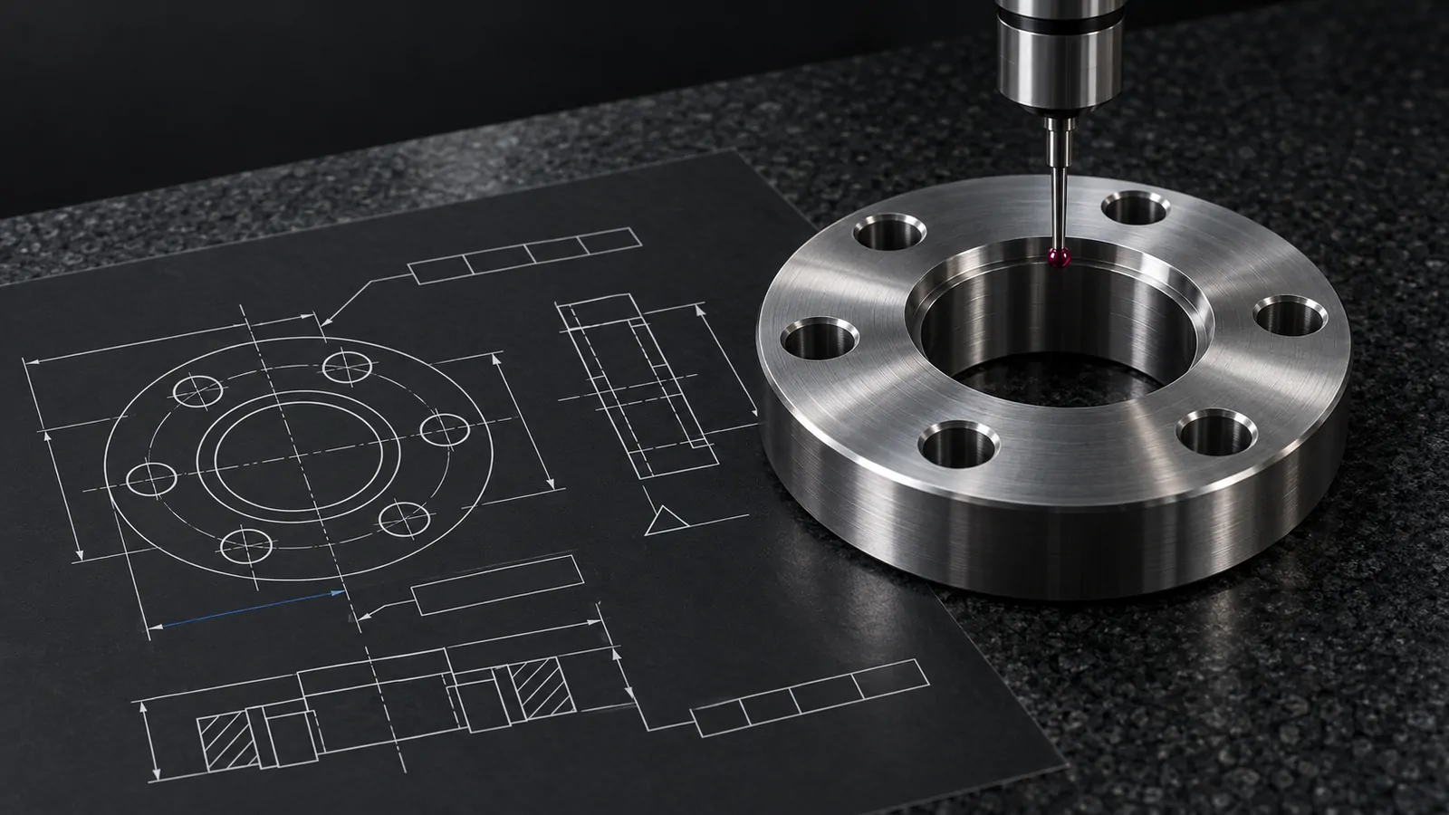
- From an "official statement" quoted by PTI: Ethereal Machines designs, develops and operates advanced CNC machines and makes high-precision components with tolerances of 2 to 20 microns. The statement adds that such parts "were traditionally manufactured in countries such as Germany and Japan".
- Not found: a formal PIB press release, any new money or scheme, or a named semiconductor customer for Ethereal. The visit restated policy. It did not announce anything new.
Ethereal Machines builds its own multi-axis CNC machine tools and sells precision machining as a service. In June 2026 it raised a $28.5 million Series B led by Avataar Ventures. The stated uses include India's first indigenous multi-axis CNC controller and "supporting semiconductor manufacturing initiatives" (Evertiq, 16 June 2026).
The remark fits a pattern. In September 2026, at SEMICON India, Vaishnaw said Indian companies had begun making machine modules that used to be imported (KNN India, 19 September 2026). Semicon 2.0 also has a whole pillar for machines and materials, covered below.
What machines does it take to make a chip?
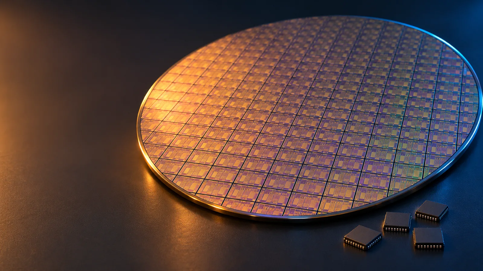
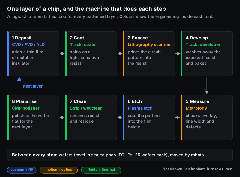
A chip is built layer by layer on a silicon wafer, 300 mm across in a modern fab. Each patterned layer goes through roughly the same loop. First a thin film is put down. Then a light-sensitive coating (resist) is spun on, the circuit pattern is printed into it, and it is developed. The result is measured, the pattern is etched into the film, the wafer is cleaned, and it is polished flat for the next layer. Each step is done by a different machine, and a fab has many of each.
| Tool family | What it does to the wafer | The engineering inside |
|---|---|---|
| Lithography scanner | Projects the circuit pattern from a mask (reticle) onto the resist | Optics, magnetically levitated stages, laser and encoder position sensing, vibration isolation, vacuum (for EUV) |
| Deposition (CVD, PVD, ALD) | Adds films of metal or insulator, from microns down to a few atoms thick | Vacuum chambers, gas delivery, RF plasma, heaters, wafer chucks |
| Plasma etch | Removes material where the resist left it exposed | Vacuum, RF power and matching, electrostatic chucks with backside cooling, chamber parts that survive plasma |
| Track (coater and developer) | Spins on resist, develops it, bakes the wafer | Precision spin motors, fluid dispense, hot plates with tight temperature control, robots |
| CMP (chemical mechanical planarisation) | Polishes the wafer flat with a pad and an abrasive slurry | Rotating heads, down-force control, slurry delivery, end-point sensing |
| Metrology and inspection | Measures line widths, overlay between layers, film thickness and defects | Optics or electron beams, precision stages, image processing |
| Wafer handling | Moves wafers between pods, tools and chambers | Robots, load ports, aligners, clean-air enclosures, vacuum robots |
The pattern to notice: apart from the chemistry and optics, these are machines. They are built from frames, chambers, bearings, motors, pumps, valves, heaters, sensors, power supplies and control software. That is why a call to build them in India is really a call to the country's mechanical, electrical and automation engineers.
What precision engineering is inside a chip-making machine?
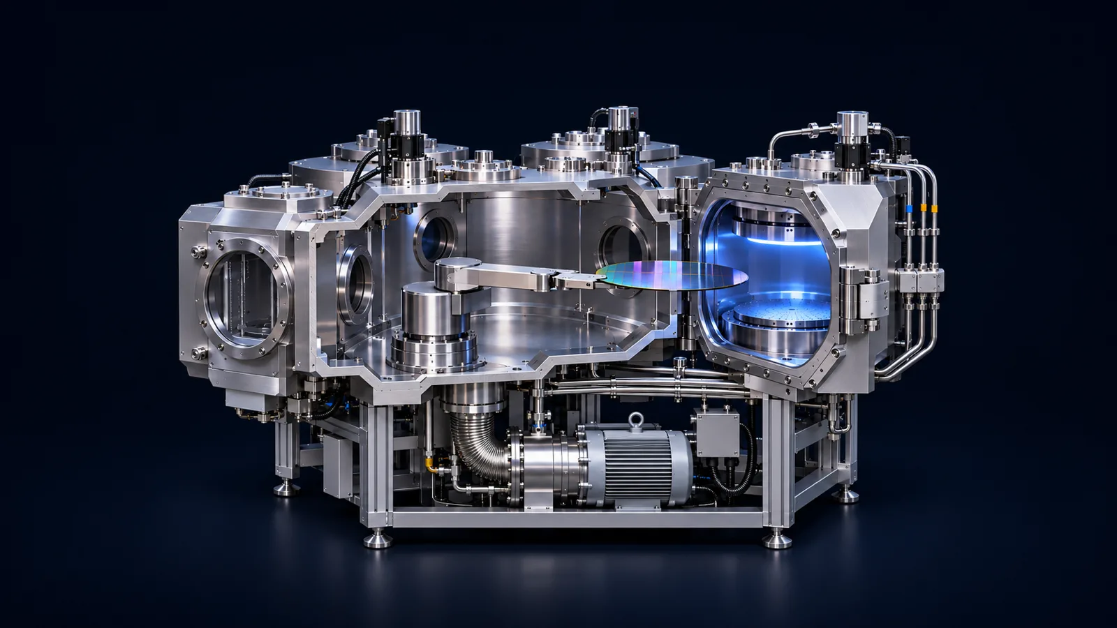
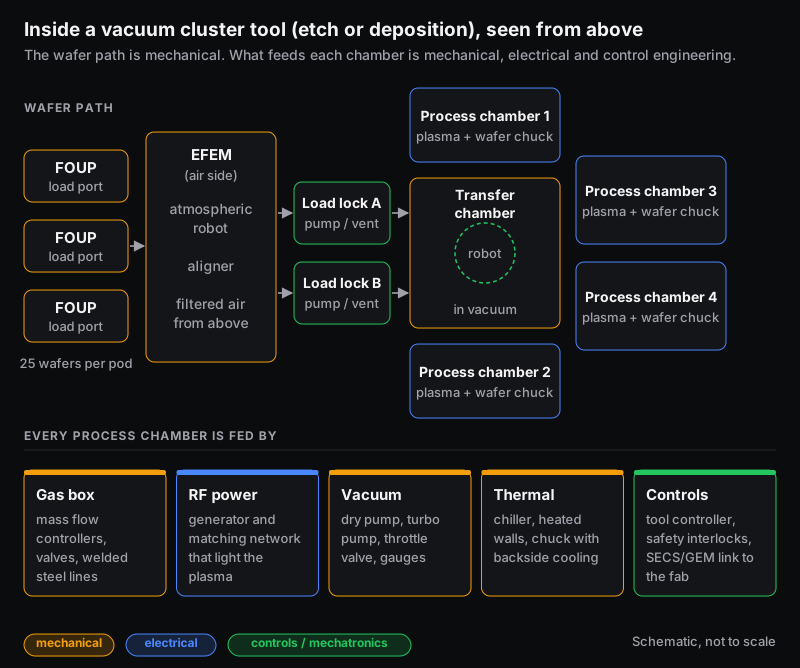
Take the most common type of machine, a vacuum cluster tool used for etch or deposition. Think of it as a small airport for wafers. The pods arrive at the gates (load ports). An air-side robot takes each wafer through a load lock, a small chamber that pumps down from air to vacuum. A second robot in a vacuum transfer chamber then hands it to one of several process chambers.
Motion and positioning
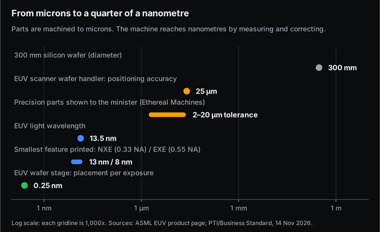
The extreme case is ASML's EUV scanner. ASML says its wafer stage places the wafer to within a quarter of a nanometre for each exposure, "checking and adjusting 20,000 times per second". Its wafer-handling robots work to a positioning accuracy of 25 µm, and they keep the wafer's surface temperature uniform to within 2 mK (thousandths of a degree) (ASML, EUV systems).
Nobody machines a part to a quarter of a nanometre. Parts are made to microns, then sensors measure where the stage really is and a control loop corrects it thousands of times a second. That is the mechatronics lesson in one sentence. The micron-level parts, like the 2 to 20 micron components shown to the minister, are the foundation that makes nanometre control possible.
Vacuum
Deposition, etch and EUV lithography all run in vacuum. EUV light is absorbed by almost everything, including air, so ASML keeps the whole light path in high vacuum. Vacuum engineering means welded and sealed stainless-steel or aluminium chambers, dry pumps backing turbomolecular pumps, throttle valves that hold a set pressure, gauges, and leak testing. It also means choosing materials that don't release gas or particles.
RF power and plasma
Etch and many deposition chambers use a plasma, a glowing gas of ions, struck by radio-frequency power. An RF generator and a matching network push that power into a load that keeps changing as the plasma changes. This is power-electronics and control work. It is a natural fit for electrical engineers.
Gas, fluid and thermal control
Process gases are metered by mass flow controllers through welded lines and valves. Resists, developers and CMP slurries are dispensed by precise pumps. Chambers, chucks and bake plates are held at set temperatures by heaters and chillers. Electrostatic chucks hold the wafer flat and remove heat through a thin layer of gas behind it. This is fluid mechanics and heat transfer, the same physics a mechanical engineer studies, applied at very tight tolerances.
Wafer handling, controls and standards
Wafers travel between tools in sealed pods called FOUPs (front-opening unified pods). A standard 300 mm FOUP holds 25 wafers (Entegris datasheet). Each tool talks to the fab's host computer through SEMI's SECS/GEM standards (SEMI). Its safety design is commonly assessed against SEMI S2, the industry's environmental, health and safety guideline for equipment (SEMI S2). Engineers who know these standards are scarce anywhere, including in India.
Who makes semiconductor equipment today?
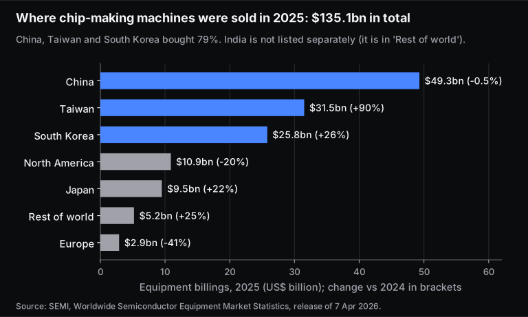
Global semiconductor equipment billings reached a record $135.1 billion in 2025, up 15% from $117.1 billion in 2024 (SEMI, 7 April 2026). The buyers are concentrated: China, Taiwan and South Korea bought 79% of it. SEMI does not list India separately.
The sellers are concentrated too. A handful of companies from the Netherlands, the US and Japan supply most of the core front-end tools.
| Company (home country) | Main tool families | Scale (latest full year) |
|---|---|---|
| ASML (Netherlands) | Lithography scanners (DUV and EUV), plus metrology and inspection. ASML describes EUV as "unique to ASML". | €32.7 billion net sales and 300 new lithography systems sold in 2025 (ASML results, 28 January 2026) |
| Applied Materials (US) | Deposition, etch, CMP, ion implant, inspection | Record $28.37 billion revenue in fiscal 2025 (Applied results, 13 November 2025) |
| Lam Research (US) | Etch, deposition, wafer clean | Not quoted here |
| Tokyo Electron (Japan) | Coater/developer tracks, etch, deposition, cleaning, wafer probers | Not quoted here |
| KLA (US) | Inspection and metrology (process control) | Not quoted here |
We have quoted revenue only where we read it in the company's own results. Behind these brand names sits a deep layer of subsystem and parts suppliers: pumps, RF generators, valves, gas systems, robots, machined chambers, ceramics and cables. That layer is where new countries usually enter, and it is where India is trying to enter now.
What does India have in semiconductor equipment today?
We found no public record of an Indian company shipping complete front-end process tools (scanners, etch or deposition systems) to a commercial fab. What is documented falls into three groups, and they carry different weight.
Confirmed policy: what Semicon 2.0 pays equipment makers
Pillar 2 of Semicon 2.0 covers machines and materials. Applications have been open since 6 November 2026. For "Manufacturing and/or Assembly of Equipment/refurbish Equipment, Sub-Assemblies, Components", the India Semiconductor Mission's scheme page lists:
| Item | Equipment, sub-assemblies, components | Equipment R&D facilities |
|---|---|---|
| Minimum capital investment | ₹300 crore | ₹300 crore |
| Minimum revenue | ₹120 crore | ₹120 crore |
| Capital support | 30% of capex, paid in step with spending (pari-passu) | 30% of capex, pari-passu |
| Production-linked incentive | 10%, 8%, 6%, 4%, 2% of the value of parts (bill of materials) bought from domestic makers, over 5 years from FY 2028-29 | None listed |
| Ceiling | "overall ceiling of 50% of the eligible capex" | Not listed |
Applicants must also "own or possess licensed technologies for the proposed unit". In practice an Indian firm needs its own design, or a licence or partnership with a global equipment maker.
Worked example. An equipment assembler invests ₹500 crore of eligible capex and buys ₹200 crore of parts a year from Indian suppliers for five years.
- Capital support: 30% × ₹500 crore = ₹150 crore.
- Production-linked incentive: ₹200 crore × (10% + 8% + 6% + 4% + 2%) = ₹20 + 16 + 12 + 8 + 4 crore = ₹60 crore.
- Total: ₹210 crore, or 42% of capex, below the 50% ceiling of ₹250 crore.
The design point is that the bonus is paid on domestic parts, not on the finished machine. That is a direct incentive to buy from Indian precision-parts makers like the one the minister visited. If local buying doubled to ₹400 crore a year, the incentive alone would reach ₹120 crore. The total would then hit the ₹250 crore ceiling, if that ceiling covers both kinds of support as "overall" suggests. The final guidelines decide.
Announced by global equipment makers (plans, not finished capacity)
- ASML and Tata Electronics signed an MoU on 16 May 2026. ASML will supply lithography systems for Tata's 300 mm fab at Dholera, and the MoU covers training, R&D and "local supply chain development" (eeNews Europe, 18 May 2026; ASML). In September, ASML's procurement chief Wayne Allan said: "We need to build a supply chain before we can do manufacturing... We are just getting started" (ANI, 17 September 2026).
- Applied Materials announced "India Vision 2035" at SEMICON India 2026. It covers about $5 billion over a decade for R&D, supplier development and talent, a 140-acre research park, and a target of ten times more India-based supply-chain capacity by 2035. Applied already has Bengaluru labs with 300 mm cleanroom capability (Evertiq, 18 September 2026; Open, 17 September 2026). These are commitments, not money spent.
- Lam Research outlined about ₹10,000 crore over the next few years. The plan includes its first silicon-component manufacturing facility in India, making parts used inside its own tools, starting from silicon ingots. Lam is talking to local firms about precision components, materials, gases, chemicals, metrology and manufacturing services. The location has not been disclosed (Business Today, 16 September 2026).
- Automation and test: Japan's Hirata is entering India through ATS India with EFEMs, load ports and wafer-handling robots. Teradyne has opened its first India office for semiconductor test in Bengaluru (same Business Today report).
Reported, not independently confirmed
- Vaishnaw said in September that Indian companies had started making machine modules that used to be imported. He also said one unnamed company exports about ₹2,000 crore of components, roughly 90% sourced from MSMEs (KNN India, 19 September 2026). No company or module was named.
- Ethereal Machines lists semiconductors among its target sectors. No semiconductor customer or part has been published.
What skills do engineers need to work in semiconductor equipment?
The work splits three ways: designing tools and subsystems (at the global equipment makers' Indian engineering centres), making parts and modules (Indian precision suppliers), and installing and maintaining tools in fabs and packaging plants. All three need the same core skills.
| Discipline | What you would work on | Skills to build |
|---|---|---|
| Mechanical | Chambers, frames, wafer-handling mechanisms, gas and cooling lines, machined and ceramic parts | GD&T and tolerance stack-ups, precision machining and inspection (CMM), vacuum design and leak testing, heat transfer, vibration and FEA, cleanroom-compatible materials, design for manufacture |
| Mechatronics / controls | Stages, robots, load ports, motion and temperature control loops | Servo and motion control, PID and feedforward tuning, sensors and encoders, PLCs and interlocks, robotics, MATLAB/Simulink |
| Electrical / electronics | RF generators, power supplies, heaters, cabling, embedded controllers | Power electronics, RF basics and impedance matching, embedded C, EMC, SEMI S2 safety and electrical design |
| All | Tool software, integration, field service | SECS/GEM equipment communication, data logging and Python, root-cause analysis, working to process recipes and SEMI standards |
A practical path for a mechanical or mechatronics graduate:
- Get fluent in GD&T. Precision suppliers are judged on whether parts meet drawings, and the minister's 2 to 20 micron example is a tolerance-and-inspection story. Our GD&T symbols guide and the GD&T course are a starting point.
- Learn one control stack end to end: a motor, an encoder, a PID loop and a PLC or microcontroller. That covers most of what a load port or robot does. The Fundamentals of Embedded Systems course helps here, and our post on mechatronics and control systems explains the basics.
- Understand the process the tool serves. You don't need to be a process engineer, but you should know why an etch chamber needs uniform temperature or why particles kill yield.
- Watch the hiring pages of equipment makers' Indian engineering centres and of the precision-parts firms that join their supplier programmes. Technician roles are growing too. Semicon 2.0 aims to train 1 lakh technicians, and a 240-hour Level 1 precision manufacturing course has been announced (KNN India, 19 September 2026).
What is the catch?
Three things temper the optimism:
- Technology is the barrier, not money. The scheme itself requires applicants to own or license the technology, and the leading tools took decades to develop. ASML says it spent more than €6 billion on EUV R&D over 17 years. Expect Indian firms to grow through parts, modules and licensed assembly first, not through complete scanners or etchers.
- Supplier qualification is slow. Equipment makers have to approve a supplier's parts before they buy them, and ASML itself says building an Indian supply chain "is going to take some time".
- The home market is still small. SEMI does not even list India as a separate equipment market. India's first silicon fab, at Dholera, is scheduled for 2028 (see our ISM 2.0 guide). So early Indian suppliers will live or die on exports to global equipment makers.
The upside is real but narrow and specific. India's best near-term opening is the precision mechanical and electromechanical layer inside these machines, which is exactly what the minister pointed at on 14 November.
Frequently asked questions
Does India manufacture semiconductor equipment?
Not complete front-end process tools at scale, as of November 2026. India has precision-parts makers and module work (reported by the government but not itemised), Indian engineering and lab centres of global equipment makers, and announced supplier programmes from ASML, Applied Materials and Lam Research. Semicon 2.0 now pays incentives to set up equipment and component manufacturing.
What exactly did Ashwini Vaishnaw announce on 14 November 2026?
No new scheme or money. During a visit to Ethereal Machines in Bengaluru, he said India should develop and make its own machines and high-precision components for semiconductor manufacturing, to reduce import dependence. PTI and IANS reported the remarks, citing a PIB Karnataka post on X.
What incentive does Semicon 2.0 give semiconductor equipment makers?
For equipment, sub-assembly and component manufacturing, 30% of capital expenditure (with a minimum investment of ₹300 crore). On top of that comes a production-linked incentive of 10%, 8%, 6%, 4% and 2% of the value of parts bought from domestic makers, over five years from FY 2028-29, with an overall ceiling of 50% of eligible capex. Source: the ISM Semicon 2.0 scheme page.
Can a mechanical engineer work in the semiconductor industry?
Yes. Chip-making machines are largely mechanical, vacuum, thermal and motion systems. Mechanical engineers design chambers and handling systems at equipment makers, make and inspect precision parts at suppliers, and maintain tools as equipment engineers in fabs and packaging plants.
Which companies make chip-making machines?
The largest are ASML (lithography), Applied Materials (deposition, etch, CMP and more), Lam Research (etch and deposition), Tokyo Electron (tracks, etch, deposition) and KLA (inspection and metrology). Global equipment billings were $135.1 billion in 2025, according to SEMI.
Sources and further reading
- Business Standard (PTI), Vaishnaw stresses need for India to make own semiconductor machinery (14 Nov 2026)
- Vartha Bharati (PTI), Vaishnaw stresses need for India to make own semiconductor machinery, components (14 Nov 2026)
- SocialNews.XYZ (IANS), India must build indigenous semiconductor manufacturing equipment ecosystem (14 Nov 2026)
- Deccan Herald, India committed to achieving self-reliance in semiconductor manufacturing (15 Nov 2026)
- India Semiconductor Mission, Semicon 2.0 scheme page (read 15 Nov 2026)
- SEMI, Global semiconductor equipment billings reached $135 billion in 2025 (7 Apr 2026)
- ASML, EUV lithography systems (read 15 Nov 2026)
- ASML, Q4 and full-year 2025 results (28 Jan 2026)
- Applied Materials, Fourth quarter and fiscal year 2025 results (13 Nov 2025)
- ASML, Tata Electronics and ASML announce strategic partnership (16 May 2026); eeNews Europe, report (18 May 2026)
- ANI via NewKerala, ASML begins local supply chain push (17 Sep 2026)
- Business Today, India's chip push goes global (16 Sep 2026)
- Evertiq, Applied Materials to invest $5 billion in India by 2035 (18 Sep 2026); Open, SEMICON India 2026: Applied Materials' $5-billion plan (17 Sep 2026)
- KNN India, Semiconductor expansion drives MSME precision manufacturing (19 Sep 2026)
- Evertiq, India's Ethereal Machines raises $28.5 million in Series B (16 Jun 2026)
- Entegris, A300 FOUP datasheet; SEMI, Introduction to SECS/GEM; SEMI, S2 EHS guideline for equipment