WEEK 6 CHALLENGE - SHIELDING VIA & DRC
Question
- On the attached example design add 2mm keepout region on the board outline and select traces and copper pour option
- Add ground copper pour on the top and bottom layer
- Add via shielding on the board end with distance between the via to be 1mm
- Run DRC and clear all errors
Your Answers
AIM:
- To add 2mm keepout region on the board outline and select traces and copper pour option.
- Add ground copper pour on the top and bottom layer.
- Add via shielding on the board end with distance between the via to be 1mm.
- Run DRC and clear all errors.
PROCEDURE:
- To add 2mm keepout region on the board outline and select traces and copper pour option.
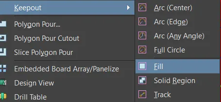
To add a keepout region click PLACE > KEEPOUT > FILL.
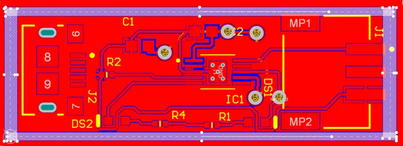
Fill the borders of the board with the keepout.
Select the keepout areas and click properties to set it as 2mm
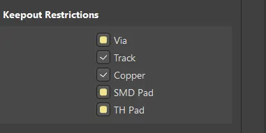
And mark traces and copper in properties.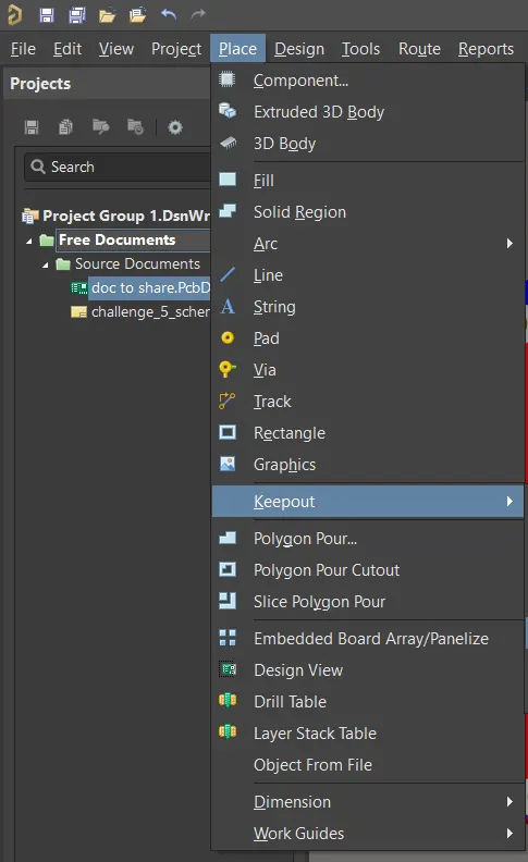
- Add ground copper pour on the top and bottom layer.
To add the copper pour select PLACE > POLYGON POUR
Add the polygon pour around the board in all sides.
select the pour and click properties to set net as GND
Then click TOOLS > POLYGON POUR > REPOUR ALL.
now the copper pour is added to the top layer.
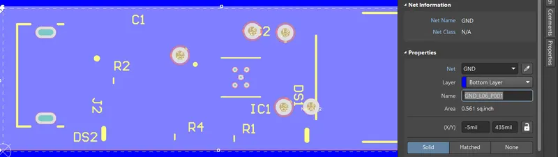
change the layer into bottom layer
Repeat the same process to add copper pour in bottom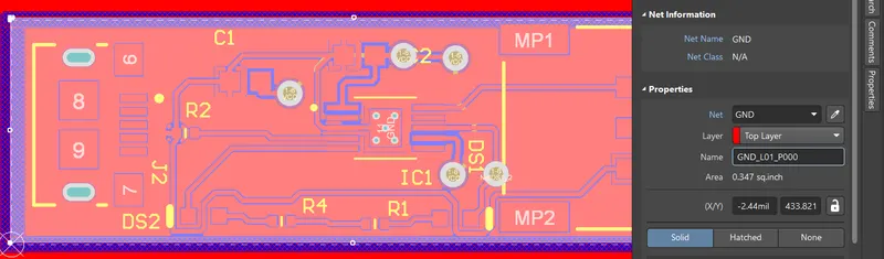
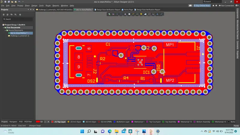
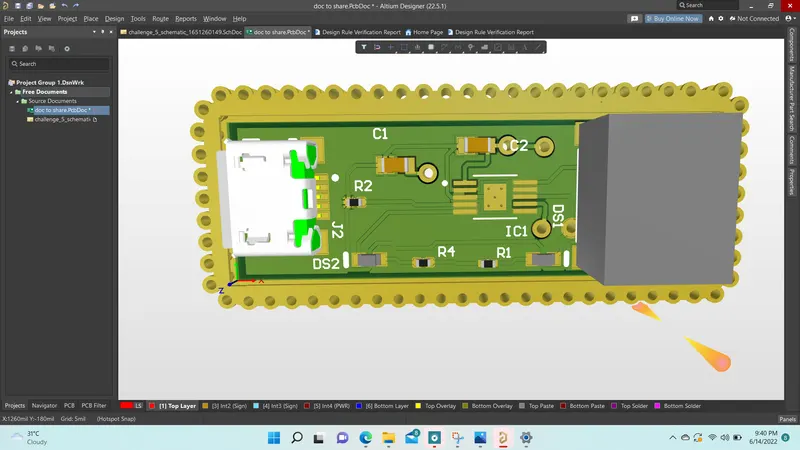
- Add via shielding on the board end with distance between the via to be 1mm.
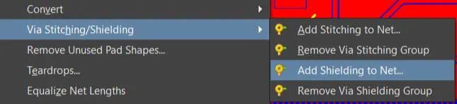
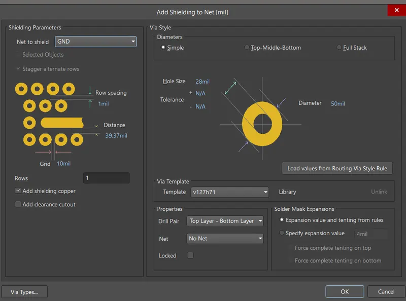
To add shielding via click TOOLS > VIA STICHING/SHIELDING > SHIELDING TO NET.
in sheilding to net set the net as GND
set the via distance is 1mm and select ok to apply it.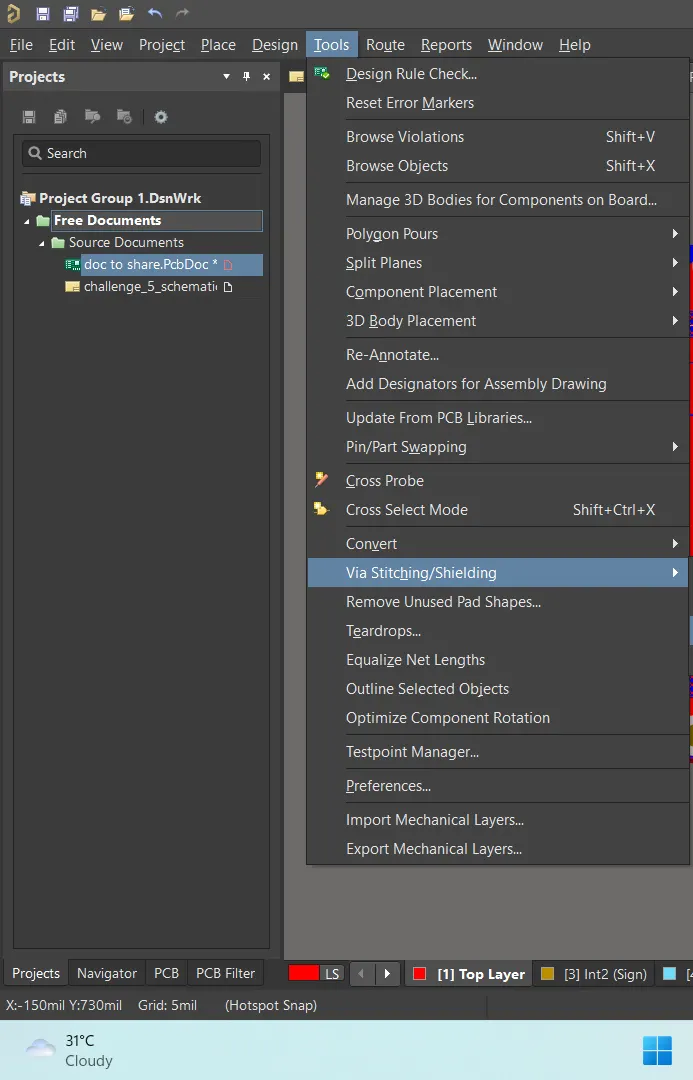
- Run DRC and clear all errors.
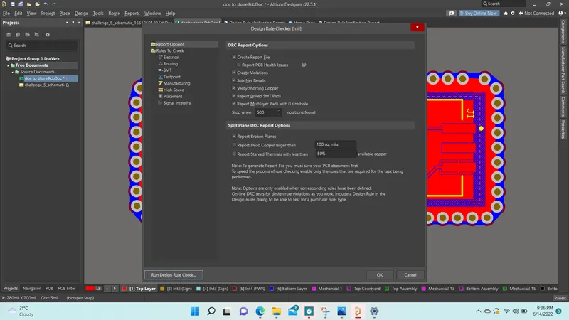
To run DRC select DESIGN > DESIGN RULE CHECK .
The popup screen will open click RUN DRC CHECK to run DRC.
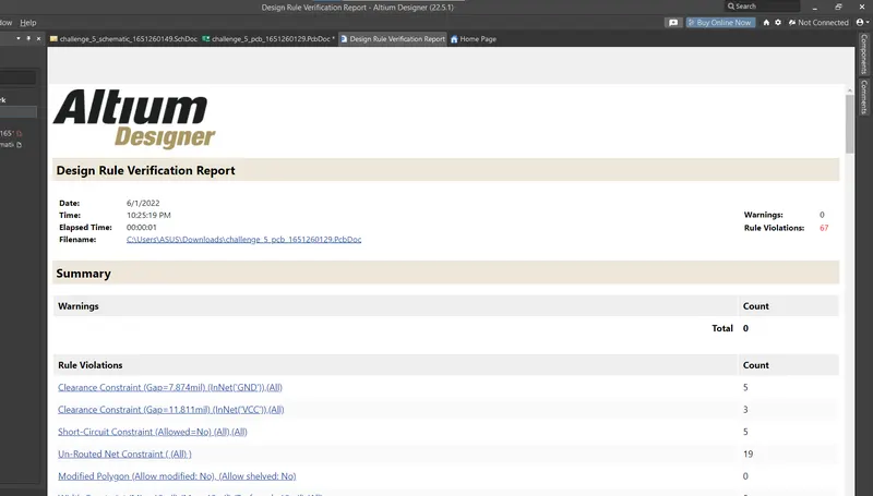
this will run and shows different types of errors
select the errors individually.
it will navigate to the particular area
most of the errors will be due to clearance it can solved in rules section by fixing the values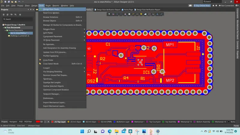
SILK SCREEN ERROR
The strings will be placed above a component or it collide with other string
we need to seperate the strings to remove this error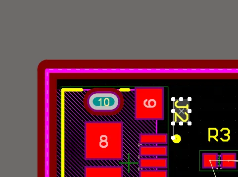
if we have additional sheet placed accidentally it will be shown up as error we need to remove it.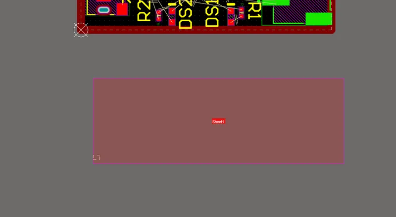
For clearance constraint in GND and VCC
select rules in design and adjust the clearance accordingly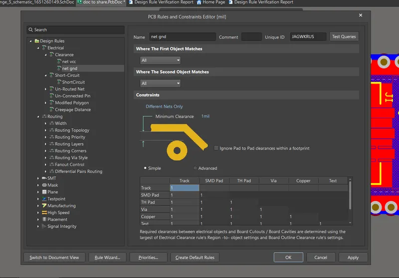
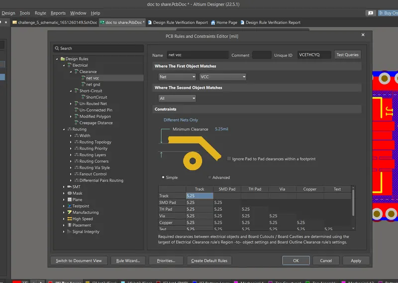
For short circuit related errors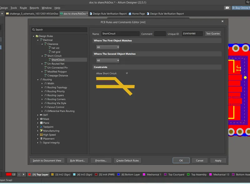
After solving out the errors again do DRC again to verify it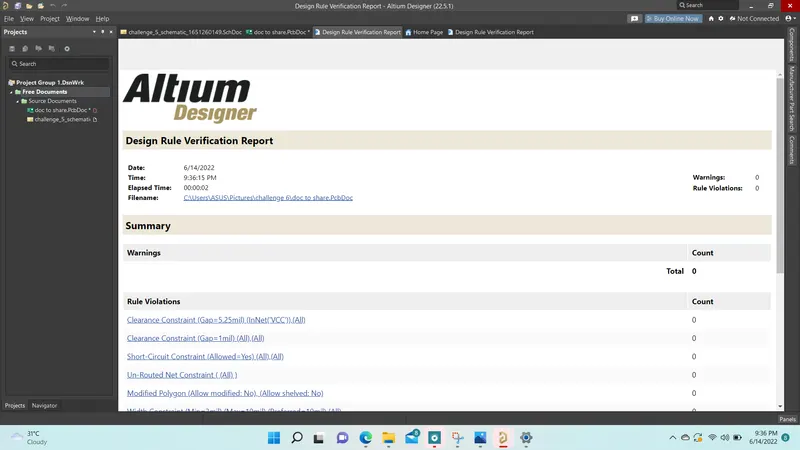
Finally save the work done.
RESULT:
- Added 2mm keepout region on the board outline and selected the traces and copper pour option.
- Added ground copper pour on the top and bottom layer.
- Added via shielding on the board end with distance between the via to be 1mm.
- DRC is run sucessfully and cleared all errors.