PROJECT 2- USE B TYPE C TO RJ45 ETHERNET
Project 2:
To design a double sided USB type C to RJ45 ethernet interface PCB utilising bus-powered
following the length matching of the high speed signals and EMC/EMI complaint.
Challenge:
- Creating a workspace for LAN7800 in altium
- Defining a PCB board size using the DXF data provided
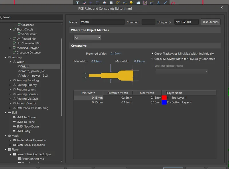
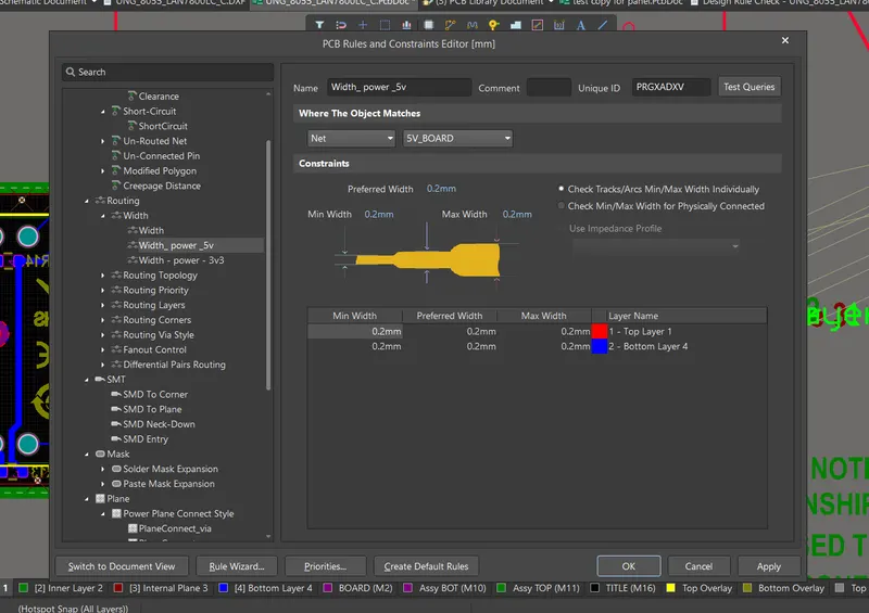
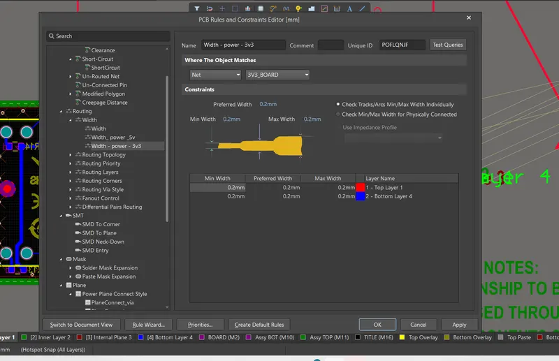
- PCB clearance to be set as 0.15mm and track width to be 0.2mm for power line and
0.15mm for rest of the circuit
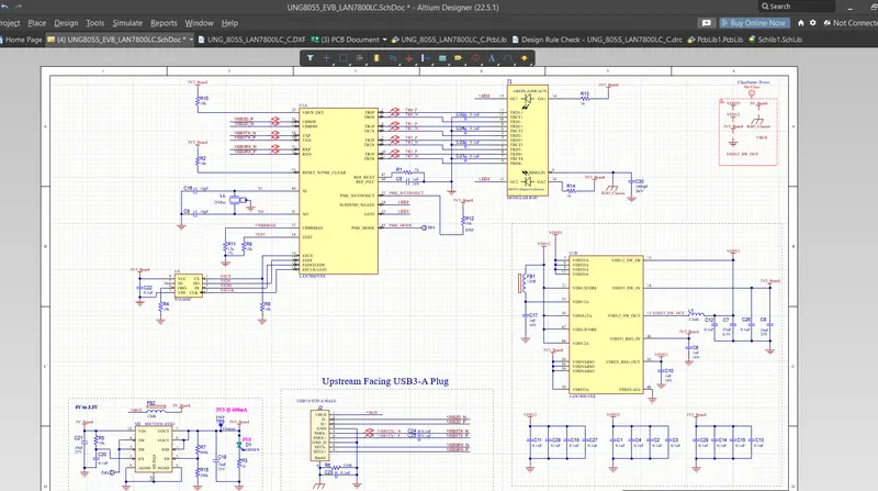
- Following the block diagram provided for creating the schematic and using the datasheet
for creating the footprint and symbol.
- Use Saturn PCB tool to find the values for 100ohm impedance for the high speed
differential pair signals
- Set PCB to 4 layer following the board stackup provided
- Identifying the key points to consider for PCB design using the datasheet
- Assemble and route the components as recommended by the datasheet
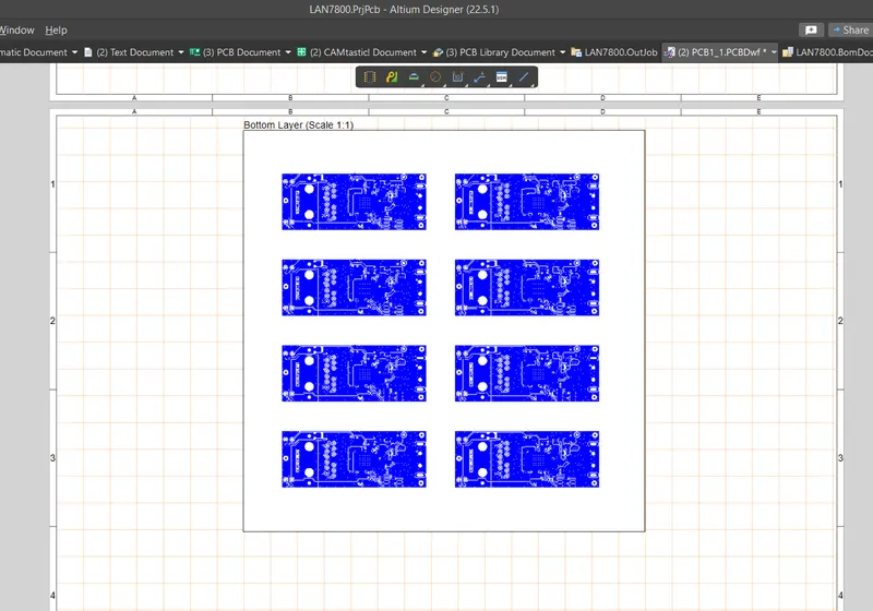
- Place the components on both the sides of the PCB and tracking on both sides.
- Add 2 fiducials diagonally opposite
- PCB board with the text (“Ethernet Interface”)
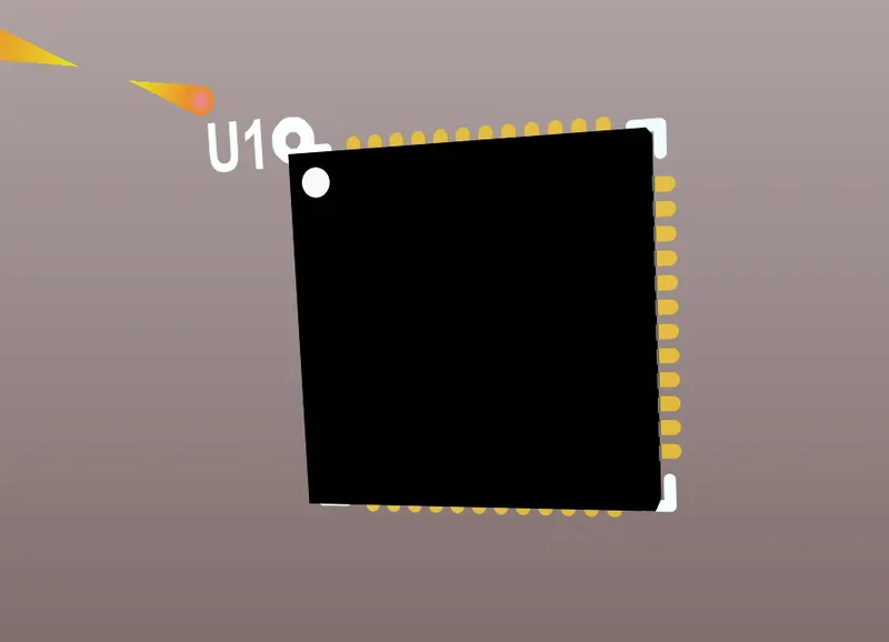
- Generate 3D files for all the components and a 3D view.
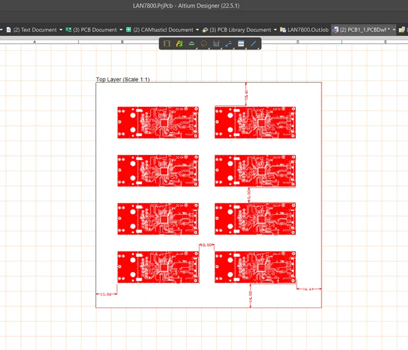
- Generate PCB panel of 150mm x 150mm and place as many circuits as possible and
follow routed method using mouse bites
- Generate complete output files for DFM and DFA (Gerber, Altium draftsman, X Y data,
BOM, assembly diagram, fabrication diagram)
PROCEDURE :
1. workplace for LAN7800 :
Step 1: open the altium designer software.
Step 2: click File > new > project.
Step 3: A popup window will popup to set the details. Enter the title as LAN7800
step 4: After adding the title, select the location where our files need to be saved.
Step 5: Finally select create option to open the project LAN7800.
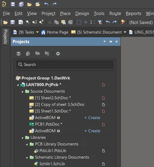
Step 6: Select project and add schematic sheet, pcb, schematic library, and pcb library.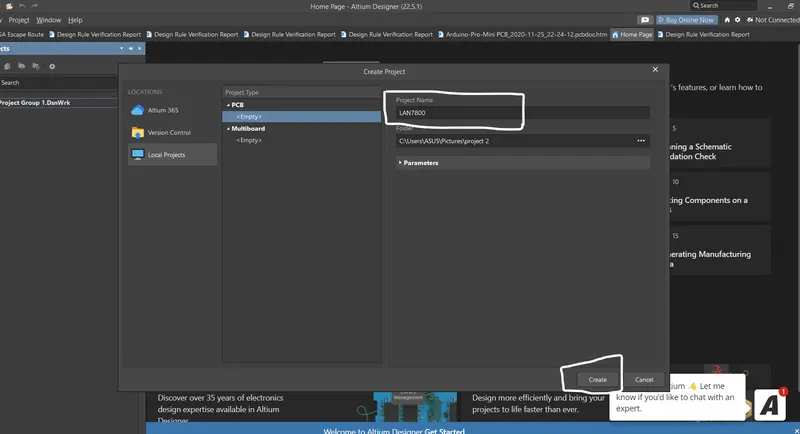
2. PCB board size :
Step 1: Enter the pcb project.
Step 2: select the reactangle option in the top bar.
Step 3: Draw the reactangle in the board.
Step 4: once completed, select the reactangle and enter properties to set the dimension as 54.74mm* 22.10mm.
Step 5: After entering the dimensions the reactangle size will be changed automatically.
Step 6: Select the created reactangle and select Board shape and define board shape from selected object.
Step 7: use the linear dimension tool which is available above the board to show the measurements by measureing the dimensions of reactangle.
Step 8: save the process.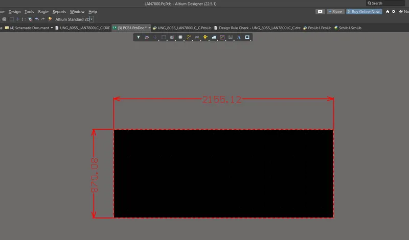
3. Pcb clearance and track width:
Step 1: To create the clearance select Design > rules in the tool bar.
Step 2: In rules navigate to clearance by typing in search bar or by finding it under electrical section.
Step 3: In the clearance set the given clearance value as 0.15mm and select apply > ok to complete the process
Step 4: once the clearance is set, navigate to routing > width in the rules section.
Step 5: select new rule and create total of 3 width rules.
Step 6: Open first width and select the net as 3v3 and set width as 0.2mm, and select apply > ok.
Step 7: open the next width rule select net as 5v and set width as 0.2mm, and select apply > ok.
Step 8: open the final width rule and select width as 0.15mm and select apply.
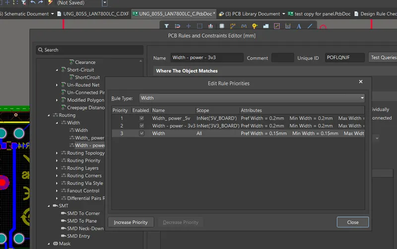
step 9: click priorities and customize it by placing the 3v3 and 5v net in the 1st two postitions,
Step10:click ok to save the process.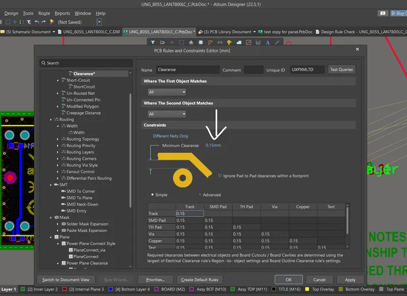
Creating Schematic :
Step 1: Search for LAN7800 in google search and find out the data sheet for that.
Step 2: Download the Datasheet. and read the datasheet completely,
Step 3: open the sheet and set the grid for 2.54mm or 1.27mm.
Step 4: Using the schematic library start creating the components.
Step 5: Once the component is created place the component in the schematic sheet.
Step 6: search for footprint to that particular component in websites like snapeda, etc to download the footprint.
Step 7: Once the footprint is downloaded select the zip file and extract that.
Step 8:click the extracted library file and import it into the component
Step 9:Select the new component and click properties and navigate to the footprint section, to check the presence of footprint.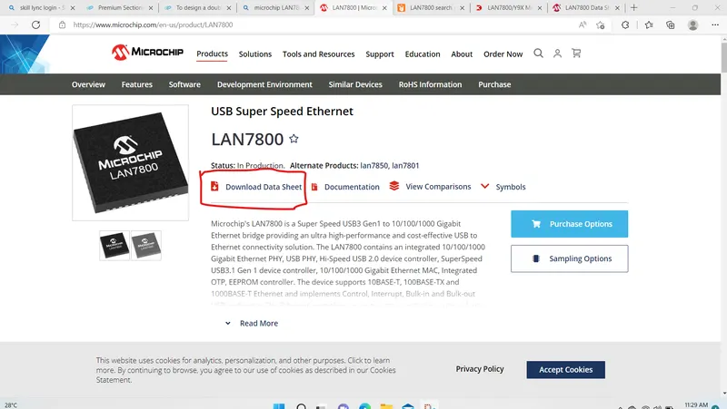
Fiducials:
Step 1: Enter the schematic sheet.
Step 2: navigate to the components section.
Step 3: In components search for fiducials and place 2 fiducials diagonally opposite to each other.
Step 4: Create a seperate box.
Step 5: Using the text option write the components name.
Step 6: save the process.
Text :
select the sheet and navigate to parameters in properties to add the parameter , title as Ethernet Interface and other parameters like date, time, author, etc.
Saturn tool :
Step 1: open the saturn pcb tool.
Step 2: enter the impendance as 100ohm.
Step 3: customize the values to get the required output.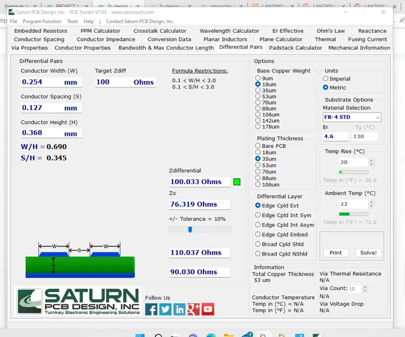
Assembling and routing:
Step 1: check the schematics was completed.
Step 2: Set up a four layer pcb.
Step 3: select validate option to check for errors.
Step 4: if there is any errors, solve the errors before moving into the next step.
step 5: select design > update pcb.
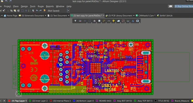
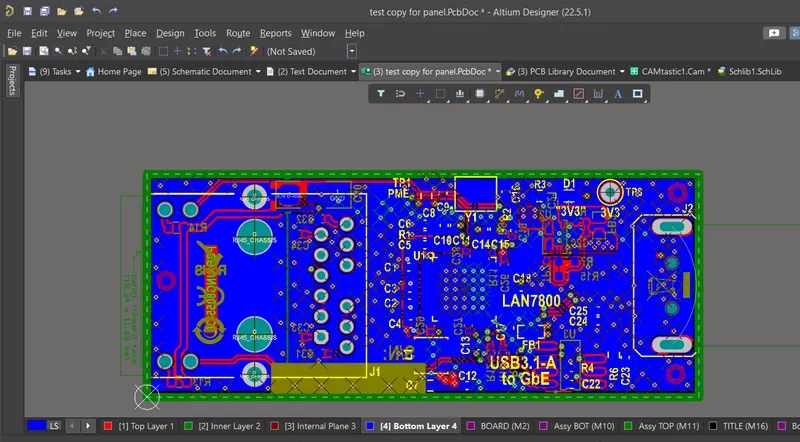
step 6: Once the option was selected the components will be automatically placed in the outer side of the board in pcb.
step 7: Arrange the components.
step 8: Use the interactive routing option to connect the traces with the help of schematic.
step 9: For differential pair use differential interactive routing to connect the components, while doing this make the lenth of postive and negative traces as same so we can avoid delays while using that in real time.
Step10: being a double sided pcb place the light weight components on the back side of pcb.
step11:Use the vias whenever needed and while using the vias set the parameter according to the net needed and connect the traces by changing into the next layer.
Step12: once the assembly process was completed use the design rule check option to figure out the erros in the circuit.
Step13: If there is any errors solve the error before going to the next stage.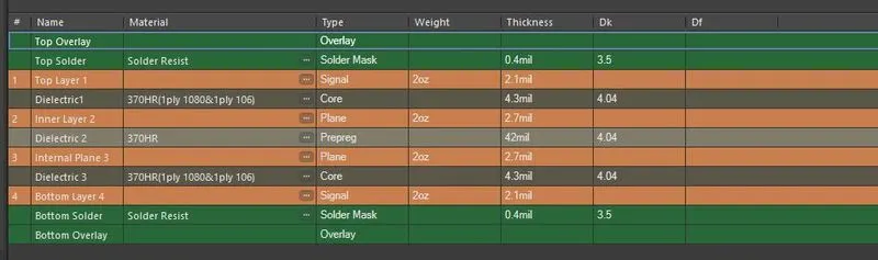
Panel :
Step 1: At first we need to add the final pcb in the altium.
Step 2: create the board outline for the pcb
Step 3:Measure the dimensions of the pcb
Step 4:After that create a new pcb project.
Step 5:In that new project customize the dimensions
Set the values for x=150mm, & y=150mm using the board outline
Step 6:one the proess is completed, select the embedded array option
Step 7:It will create a section to add the pcb
Step 8:Add the pcb in that particular section.
Step 9:After getting the numbers, enter the values in the respective areas in the properties,
Step10:we need to ensure the distance of 10mm should be maintained betwwen the pcb and between the pcb and margin.
Step11:For doing the above process we need to customize the values in the properties.finally the pcb will be aligned automatically
Step12:once the above process is completed, we need to cross verify the dimension by measuring them.
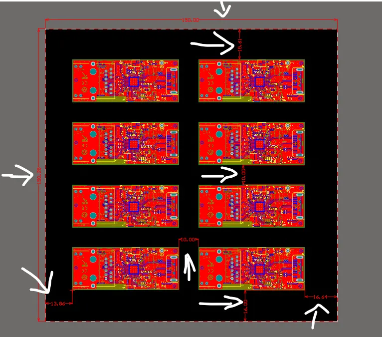
As the next step we can enter into the next step for seperating the individual pcb in the panel, for that process we can two different methods to handle it.
1.v scoring
2. mouse bite
vscoring is a process of seperating the individial pcb by adding the v scoring component from the explorer and placing it between the individual pcb.
This is most recommended method for seperation of individual circuits because it eliminates the issues of damaging the components in the layer and also holds the panel better while fabricating.
mouse bite is the another process for seperating the individual circuits by adding a halogen space around the circuit and adding mouse bite component from the explorer which looks like rings in 4 or more areas surrounding the circuit.
usually while adding the mouse bites it has some constraint like we cant add these near to via and in designing high density complex board it will be quiet difficult to choose the area to place the mouse bites.
DMF & DFA :
Step 1: once all the verifications process is completed, we need to start generating the documents for fabrication and assembly.
Step 2: select files > fabrication output > gerber files.
Step 3: select files > fabrication output > ns drill.
Step 4: select files > assembly output > assembly drawings.
Step 5: select files > assembly output > generate pick and place files.
Step 6: select files > assembly output > test points.
Step 7: select files > smart pdf
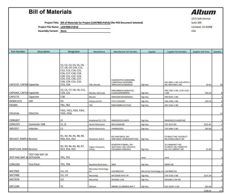
Step 8: select report > bill of materials.
Step 9: after selecting that select currency to inr and give preview to view the report and select add to project to create a active bom.
step 8: select project (LAN7800) > draftsman.
Step 9: in draftsman attach pcb with view from different layer and attach other datas like bom, x&y plane , etc.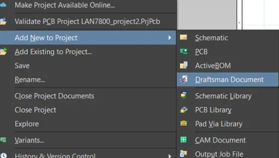

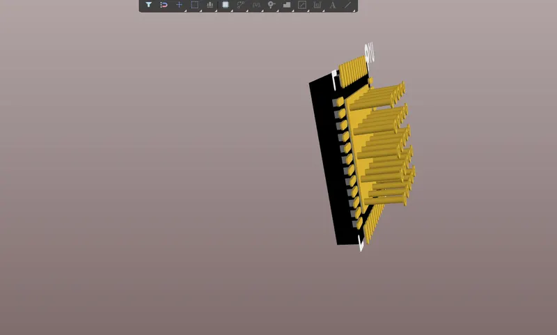
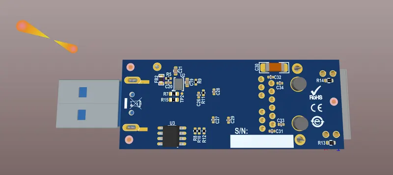
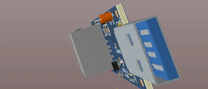
RESULT :
Designed a double sided USB type C to RJ45 ethernet interface PCB utilising bus-powered following the length matching of the high speed signals and EMC/EMI complaint.