PROJECT 1: LDO 5V INPUT, STEPPING DOWN TO 3V3
Project 1:
To design a PCB using Altium ECAD software for a low dropout voltage regulator (LDO) for 5V input, stepping down to 3.3V
Challenge:
- Creating a workspace for MIC33030_3V3
- Defining a PCB board size of 40mm x 40mm for a 2 layer PCB
- PCB clearance to be set as 0.2mm and track width to be 0.3mm for power line and
0.2mm for rest of the circuit
- Following the block diagram provided for creating the schematic and using the
datasheet for creating the footprint and symbol.
- Molex 3 pin 2.54mm connector on the input and 2 pin connector on the output
- Identifying the key points to consider for PCB design datasheet
- Assemble and route the components as recommended by the datasheet
- Add 4 mounting holes (3mm) on all corners with 2 fiducials diagonally opposite
- PCB board with the text (“DC-DC Power Supply – Rev1”)
- Input connector – text “Input 5V” “Ground” and “Enable”, Output connector – text
“Output - 3.3V” “Ground”
- Copper pour added on the top and bottom layer for ground net and all passive
components with thermal relief
PROCEDURE :
1. workplace for MIC33030_3v3 :
Step 1: open the altium designer software.
Step 2: click File > new > project.
Step 3: A popup window will popup to set the details. Enter the title as MIC33030_3v3
step 4: After adding the title, select the location where our files need to be saved.
Step 5: Finally select create option to open the project MIC30330_3v3.
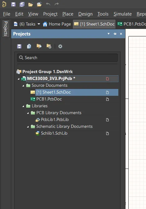
Step 6: Select project and add schematic sheet, pcb, schematic library, and pcb library.
NOTE: MIC30330 REPRESNT THE COMPONENT AND 3V3 RESPRENTS THE 3.3V 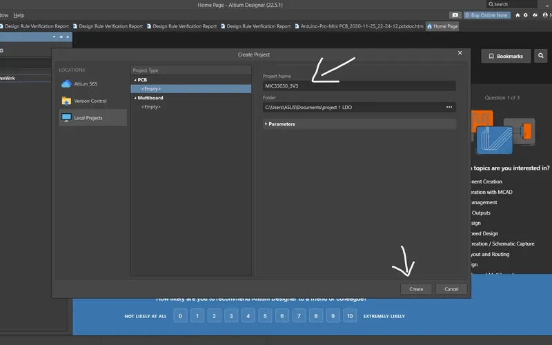
2. PCB board size :
Step 1: Enter the pcb project.
Step 2: select the reactangle option in the top bar.
Step 3: Draw the reactangle in the board.
Step 4: once completed, select the reactangle and enter properties to set the dimension as 40 * 40mm.
Step 5: After entering the dimensions the reactangle size will be changed automatically.
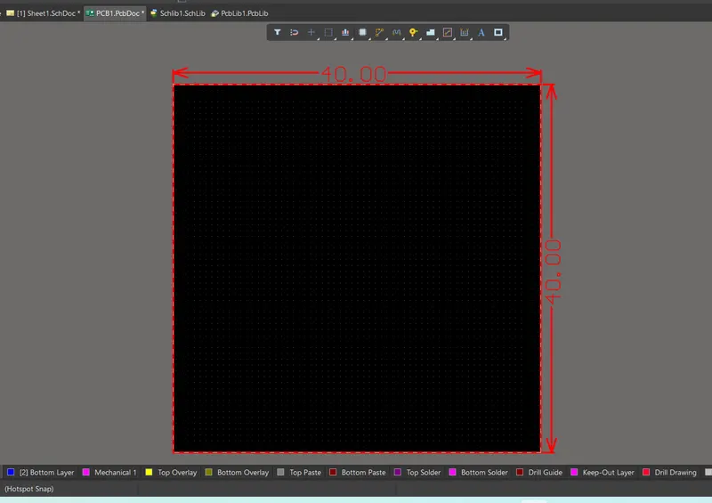
Step 6: Select the created reactangle and select Board shape and define board shape from selected object.
Step 7: use the linear dimension tool which is available above the board to show the measurements by measureing the dimensions of reactangle.
Step 8: save the process.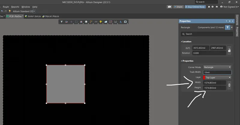
3. Pcb clearance and track width:
Step 1: To create the clearance select Design > rules in the tool bar.
Step 2: In rules navigate to clearance by typing in search bar or by finding it under electrical section.
Step 3: In the clearance set the given clearance value as 0.2mm and select apply > ok to complete the process
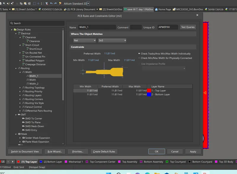
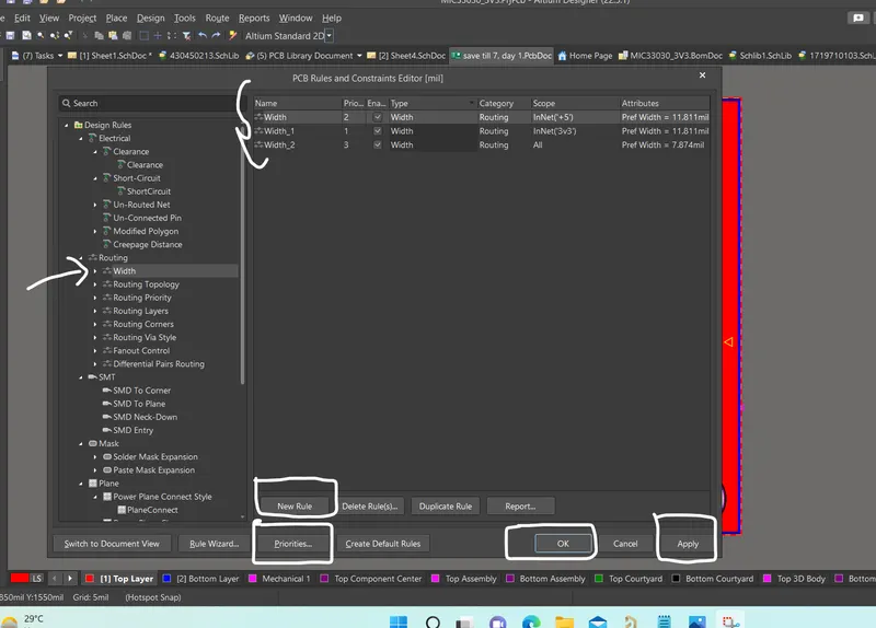
Step 4: once the clearance is set, navigate to routing > width in the rules section.
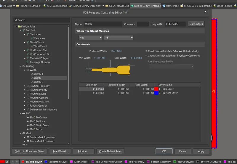
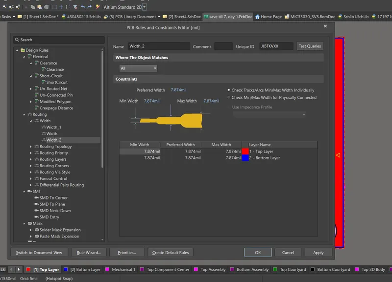
Step 5: select new rule and create total of 3 width rules.
Step 6: Open first width and select the net as 3v3 and set width as 0.3mm, and select apply > ok.
Step 7: open the next width rule select net as 5v and set width as 0.3mm, and select apply > ok.
Step 8: open the final width rule and select width as 0.2mm and select apply.
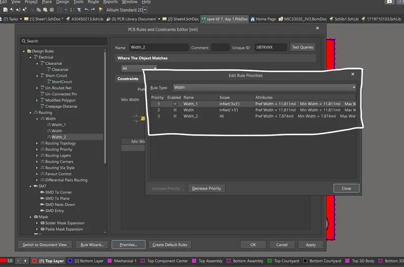
step 9: click priorities and customize it by placing the 3v3 and 5v net in the 1st two postitions,
Step10:click ok to save the process.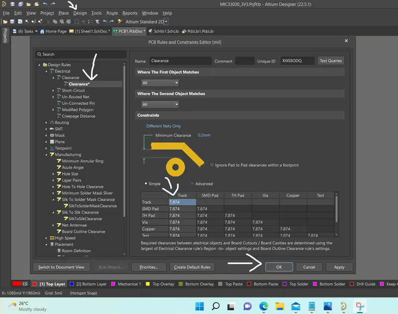
4. Creating Schematic & Footprint:
Step 1: Search for MIC30330 in google search and find out the data sheet for that.
Step 2: Download the Datasheet.
Step 3: Read the datasheet completely, because their will different type of varients will be available with different packages.
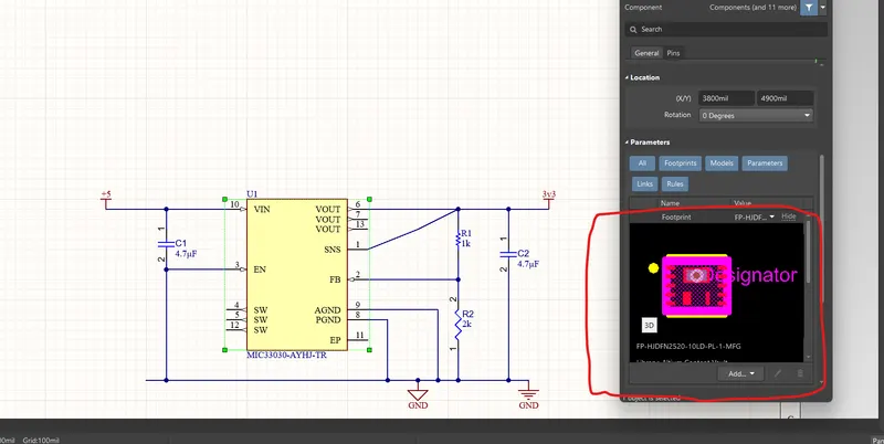
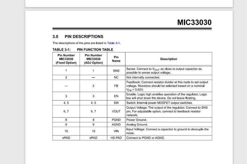
Step 4: For MIC33030 we have two varient in the datasheet, one with fixed output and the second with adjustable output, for our schematic we are looking for 3.3v output, the fixed output has a different ouutput value so we can go for the adjustable ouput varient to get the desired output of 3v3.
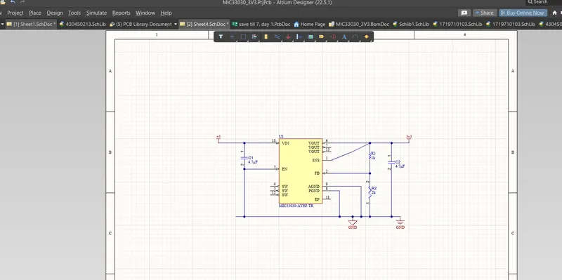
Step 5: Figure out the correct schematic symbol for the adjustable varient in the datasheet.
Step 6: open the sheet and set the grid for 2.54mm or 1.27mm.
Step 7: Using the schematic library start creating the components.
Step 8: Once the component is created place the component in the schematic sheet.
Step 9: search for footprint to that particular component in websites like snapeda, etc to download the footprint.
Step10: Once the footprint is downloaded select the zip file and extract that.
Step11:click the extracted library file and import it into the component
Step12:Select the new component and click properties and navigate to the footprint section, to check the presence of footprint.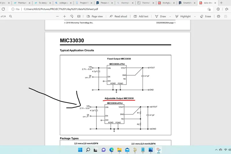
5. Molex:
Step 1: using the schematic library add the 3pin molex in that by creating by our own or by importing symbol from websites.
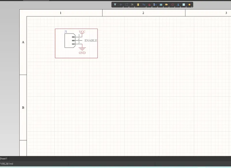
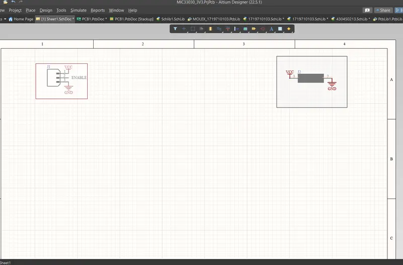
Step 2: once the component is created place tha component in sheet and add the Gnd and power ports acordingly.
step 3: Add the footprint of the molex 3pin.
Step 4: similarly create molex 2pin by following the above procedures.
step 5: save the process.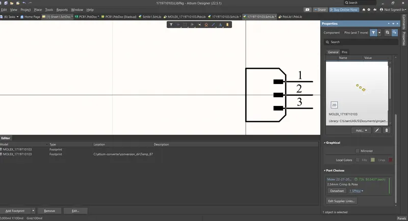
6. connector details:
After adding the molex connector in the schematic add the designators and names accordingly like, 5v. 3v3, ground and enable for the respective molex connectors ( The reference images are attached with challenge 5 ).
7. fiducials and mounting holes:
Step 1: Enter the schematic sheet.
Step 2: navigate to the components section.
Step 3: In components search for fiducials and place 2 fiducials diagonally opposite to each other.
Step 4: After completing that search for mounting holes and place 4 mounting holes in the sheet.
Step 5: Create a seperate box for both.
Step 6: Using the text option write the components name.
step 7: save the process.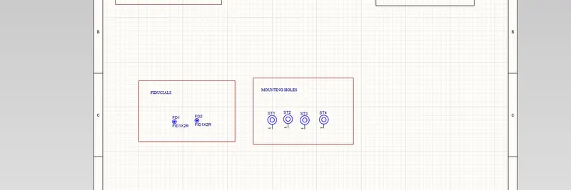
8. Text :
select the sheet and navigate to parameters in properties to add the parameter revision 1, title as DC-DC convertor and other parameters like date, time, author, etc.
9.Datasheet:
Datasheet is a document consists the important details of the component for designing.
Step 1: Download the datasheet from the manufactures website like texas instruments, etc.
Step 2: Once the process was completed open the document.
Step 3: navigate to the schematic section where we can identify the schematic for that particular component.
step 4: There will be different varients will be available, Depends on our requirement select the perfect varient and note down the package type.
Step 5: After that process we can create the schematics in our project using the schematic given given in the datasheet.
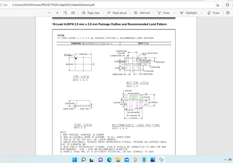
Step 6: To create the footprint we need to navigate to that particular page which consists the details of that selected package.
Step 7: Using the given measurements we can generate our own foorprint by using IPC complaint footprint wizard in altium.
Step 8: And the datasheet contains some other information like temperature, pin descriptions, etc to check before starting the design.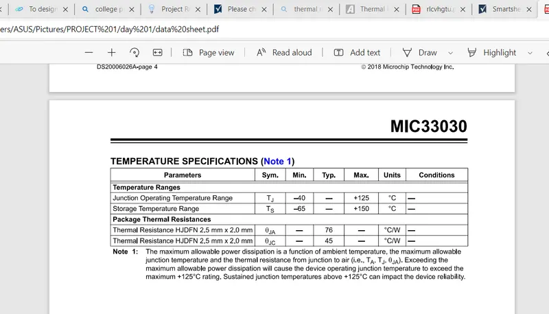
10. Assembling and routing:
Step 1: check the schematics was completed.
Step 2: select validate option to check for errors.
Step 3: if there is any errors, solve the errors before moving into the next step.
step 4: select design > update pcb.
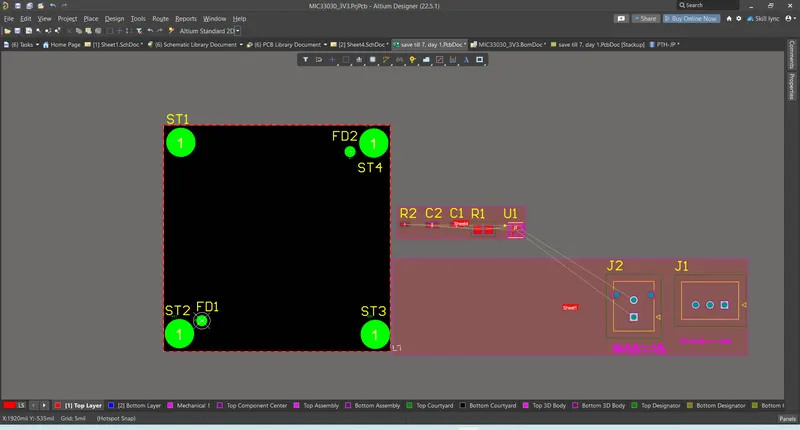
step 5: Once the option was selected the components will be automatically placed in the outer side of the board in pcb.
step 6: Arrange the components.
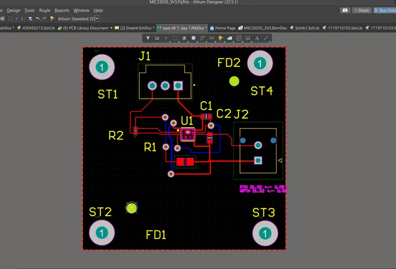
step 7: Use the interactive routing option to connect the traces with the help of schematic.
Step 8: Use the vias whenever needed and while using the vias set the parameter according to the net needed and connect the traces by changing into the next layer.
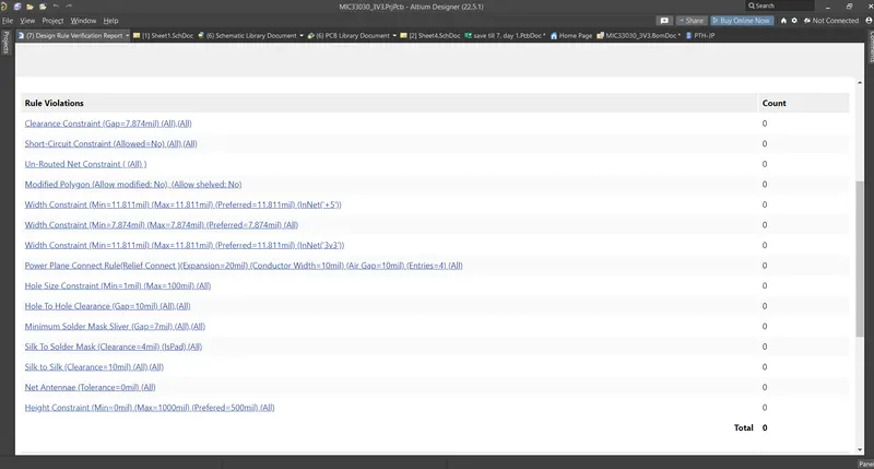
Step 9: once the assembly process was completed use the design rule check option to figure out the erros in the circuit.
Step10: If there is any errors solve the error before going to the next stage.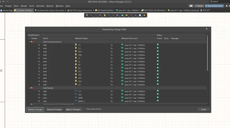
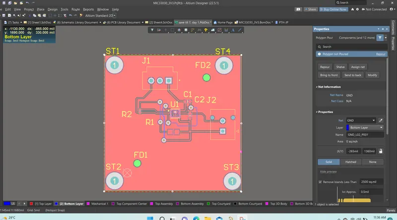
11. copper pour:
Step 1: Enter the pcb project section.
Step 2: Select the polygon pour and draw the polygon over the top layer of the board.
Step 3: After completely covering the top layer select the properties and set the net as GND.
Step 4: Select the polygon pour option in tools bar and select repour all to add the copper pour in the top layer.
Step 5: change the layer from top to bottom and repeat the above process tp add the copper pour on the bottom layer,
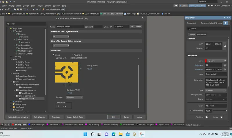
Step 6: once the process is completed add the thermal relief to the passive components in the pcb board.
step 7: By navigating to plane under design rules we can customize the rules for thermal relief.
step 8: save the project.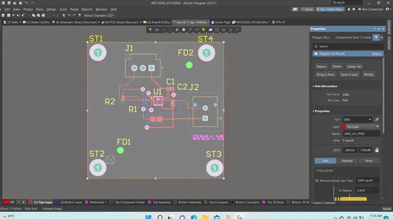
FINAL PCB :
TOP VIEW :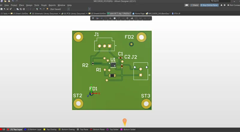
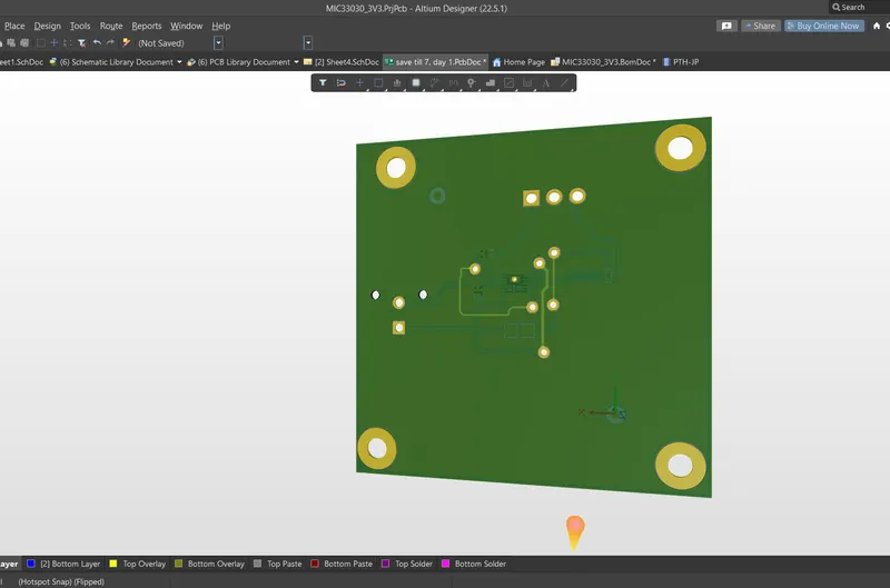
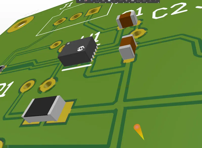
RESULT :
Designed a PCB using Altium ECAD software for a low dropout voltage regulator (LDO) for 5V input, stepping down to 3.3V.