WEEK 11 CHALLENGE- PANELIZATION
Question
- Use the provided PCB to create a panel that can contain the maximum number of circuits by following the panelization rule.
- Using the provided gerber data, overlap the two gerber data sets and identify the issues on each layer.
Your Answers
AIM:
To use the provided PCB to create a panel that can contain the maximum number of circuits by following the panelization rule.
To use the provided gerber data, overlap the two gerber data sets and identify the issues on each layer.
PROCEDURE:
1.PANELIZATION:
panelization is a process of grouping the individual circuits with same layer stack setup and with or without different shapes to reduce the time for fabrications.
At first we need to add the final pcb in the altium.
create the board outline for the pcb
Measure the dimensions of the pcb
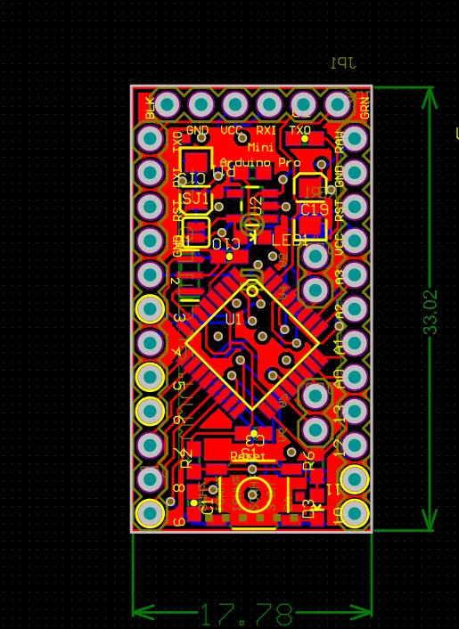
After that create a new pcb project.
In that new project customize the dimensions
Set the values for x=430mm, & y=585mm using the board outline
one the proess is completed, select the embedded array option
It will create a section to add the pcb
Add the pcb in that particular section.
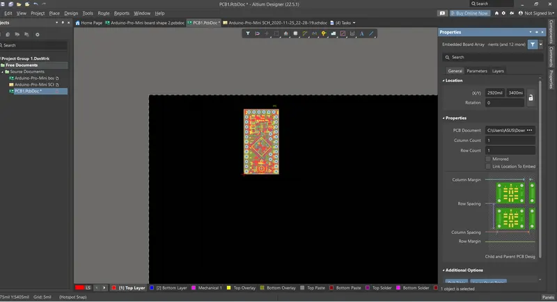
Now we need to calulate the no.of rows and columns in the panel
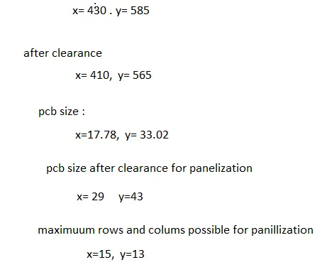
After getting the numbers, enter the values in the respective areas in the properties,
we need to ensure the distance of 10mm should be maintained betwwen the pcb and between the pcb and margin.
For doing the above process we need to customize the values in the properties.
finally the pcb will be aligned automatically
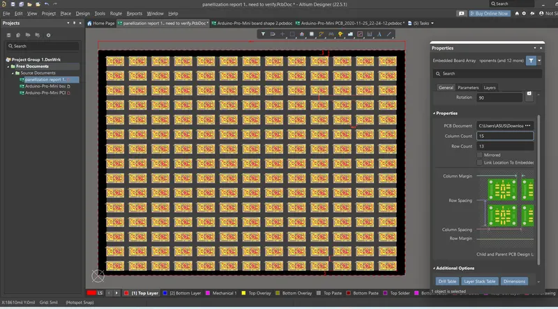
once the above process is completed, we need to cross verify the dimension by measuring them.
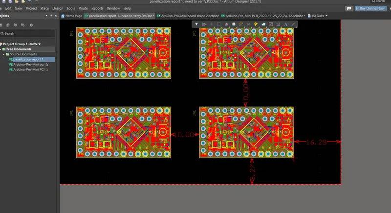
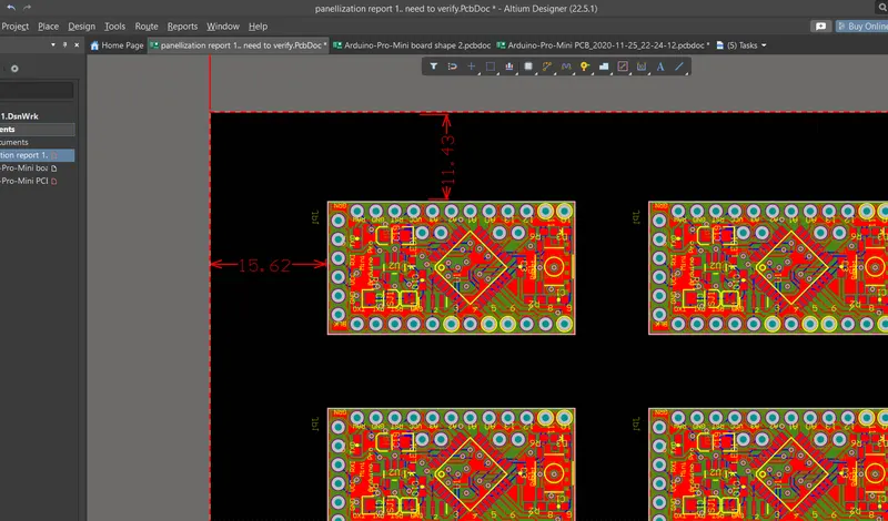
If we get the proper distance in the panel we can move into the next step for gerber generation.
By selecting the option file> fabrication output> gerber file.
We need to select the milimeter and select the least available ratio in the first section.
In the second section select the used on option to get only the layers what we created and used here.
after these process checkout the checkboxes in the third page and click ok in the final.
Now we generated the required the gerber file.
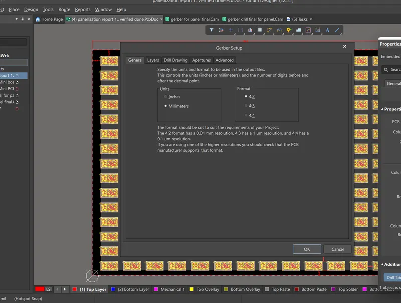
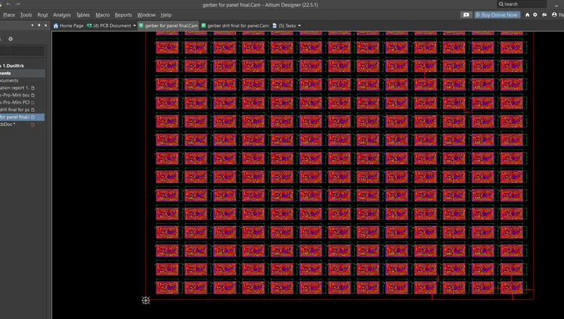
similarly we need to create the ns drill for the panel, by selecting file> fabrication output> ns drill.
But here we need to click the inches in length and select the least available ratio
And finally generate the drill file
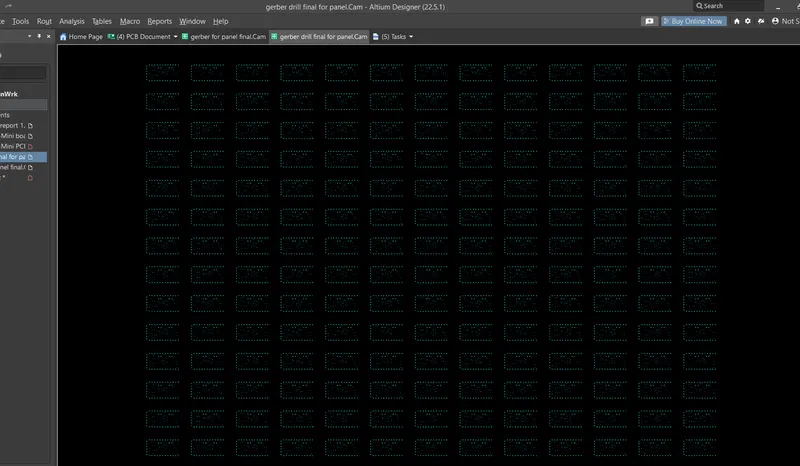
For cross verifying the layers we have a separate software named as viewmate.
For using this pcb in viewmate software we need to extract the gerber file from the panel.
By selecting the options export> gerber and clicking ok we can get the files for all the individual layers.
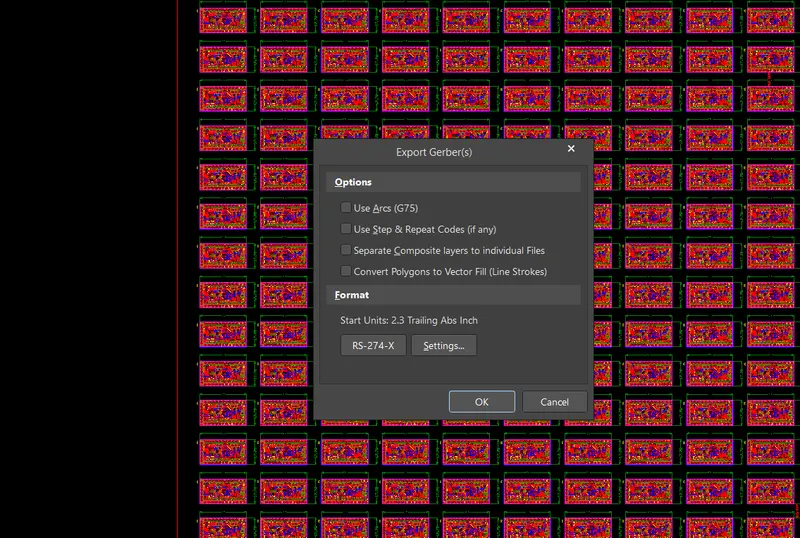
we can drag these files from the file manager where we stored and paste it in the left side of the viewmate.
Now we can see all the individual layers by switching on and off between the layers to track the overlaping.
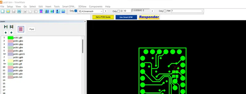
After doing this process we need to fiigure out the layers which are needed for fabrication process.
The layers like gtl,gbl,gtp,gbp,gts,gbs,gto,gbo, etc are selected seperately in the file manager and we need to create a zip file for that.
We need to do the same process like creating gerber, ns drill nd export gerber for individual pcb file also.
2.OVERLAY:
once we created the zip fil for the individual pcb, we can drag and paste the zip in the viewmate software.
The layers will be shown there automatically.
Now we need to verify the layers By switching on and off between different layers to identify the issues.
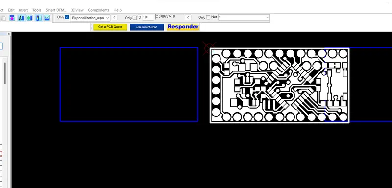
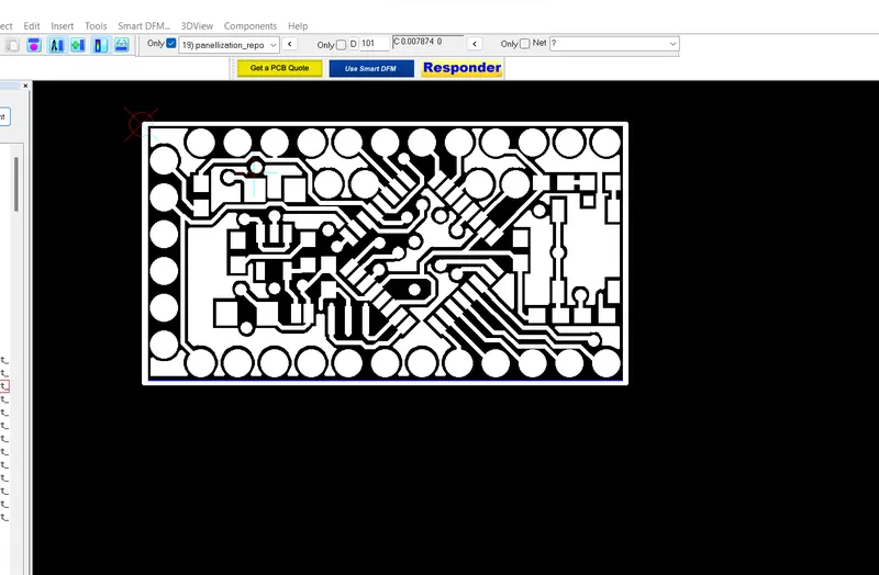
In the above image the individual pcb layer is overlap with the board outline to check the issues in the dimensions,and the overlaping result is shown.
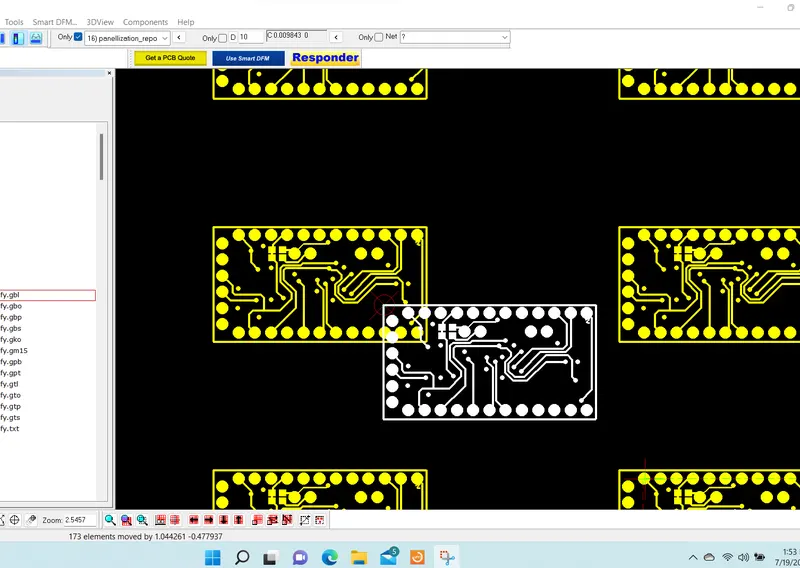
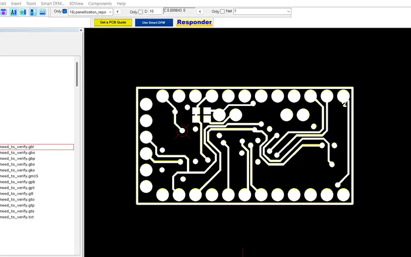
In the above image the bottom layer of individual pcb is overlaped with one of the circuit in panel with bottom layer.
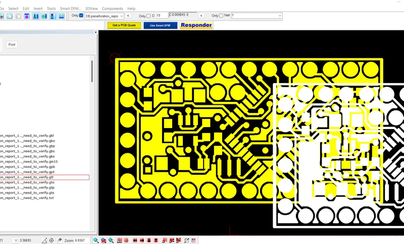
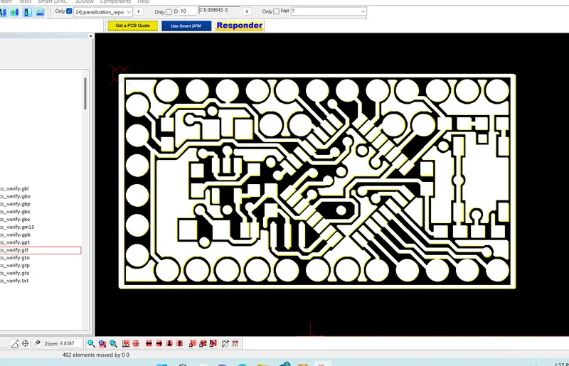
In the above image the top layer of individual pcb is overlaped with one of the circuit in panel with top layer.
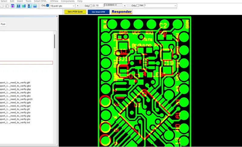
In the above image we can clearly see there is overlap issue with the components and the existing texts.
so, in this case the designer need to get back to the pcb in altium, and need to customize the texts accordingly to eliminate this type of issues.
If the designer send this file to fabrication without doing the changes, in the final output some of the texts will not be printed properly.
After the issue is sorted out , we need to repeat the process from panelization to viewmate again.
Once the layers are verified with no errors, As the next step we can enter into the next step for seperating the individual pcb in the panel, for that process we can two different methods to handle it.
1.v scoring
2. mouse bite
vscoring is a process of seperating the individial pcb by adding the v scoring component from the explorer and placing it between the individual pcb.
This is most recommended method for seperation of individual circuits because it eliminates the issues of damaging the components in the layer and also holds the panel better while fabricating.
mouse bite is the another process for seperating the individual circuits by adding a halogen space around the circuit and adding mouse bite component from the explorer which looks like rings in 4 or more areas surrounding the circuit.
usually while adding the mouse bites it has some constraint like we cant add these near to via and in designing high density complex board it will be quiet difficult to choose the area to place the mouse bites.
RESULT:
Used provided PCB to create a panel that can contain the maximum number of circuits by following the panelization rule.
Used the provided gerber data, to overlap the two gerber data sets and identifed the issues on each layer.