Project 3
Aim:
Design and simulation of Buck converter for Auxiliary load in EV.
- Input voltage is 48V, Output voltage is 12 V
- Load current is 10A
- Calculate Duty ratio and Load(use Resistor as Load)
- Calculate L,c
Design:
From the given information
duty ratio=Vout/Vin
we can take switching frequency=500000Hz (assume)
there fore duty ratio=12/48= 0.25 or 25%
Load Resistance=Vout/Iout=12/10=1.2ohm
Inductor selection:
delta IL = estimated inductor current which is 20 to 40% of output current .
L=[vo(1-D)/fs* delta IL )]
delta IL=(0.2-0.4)*Iout max
=0.2*10=2A
then L=12 (1-0.25)/500000*2= 9*10^-6Henry
Capacitance selection:
Cout=delta I out/ 8fs delta vout
= 2/(8*500000*0.02)
=2.5*10^-5Farad
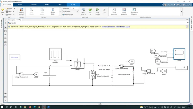
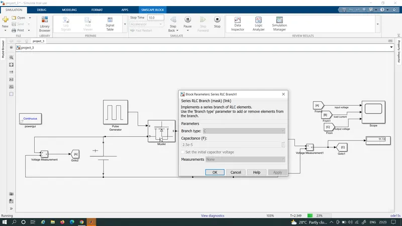
Simulation of Buck converter is done as shown above
Block used:Battery,Pulse generator,MOSFET,Diode,Inductance,Capacitance,Resistance Current measurement,voltage measurement,scope and power gui
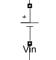
Battery:Battery is used to provide input dc voltage of 48V.
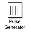
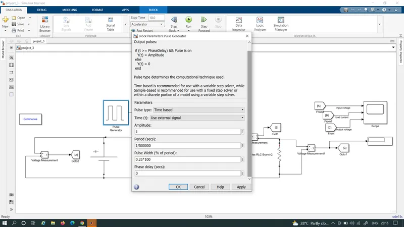
Pulse generator:In pulse generator we set switching fequency 500000Hz and pulse width 25% and fed to MOSFET
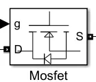
MOSFET:We use mosfet as switching device here and keep the default paramter.
MOSFETs are for power switching circuits. Unlike bipolar junction transistors (BJTs), the competing type of power transistor, MOSFETs do not require a continuous flow of drive current to remain in the ON state. Additionally, MOSFETs can offer higher switching speeds, lower switching power losses, lower on-resistances, and reduced susceptibility to thermal runaway.
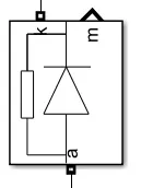
Diode:kept the diode parameter same.
Capacitance:capacitance value set to 2.5*10^-5Farad
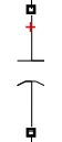
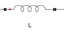
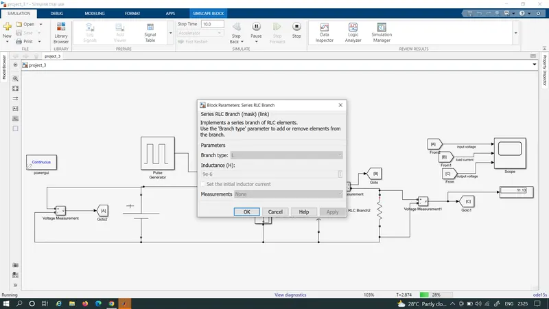
Inductance:Inductance value set to 9*10^-6 Henery
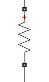
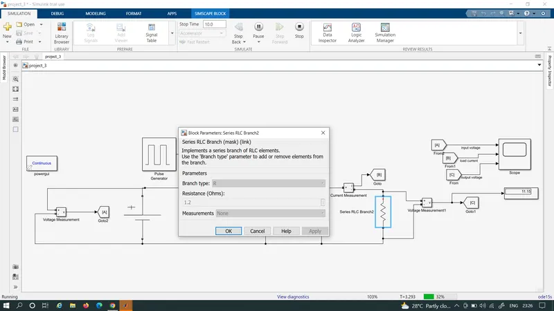
Resistance:Resistance value set as 1.2ohms
The working of a buck converter can be broken down into a few steps.
STEP – 1:
The switch turns on and lets current flow to the output capacitor, charging it up. Since the voltage across the capacitor cannot rise instantly, and since the inductor limits the charging current, the voltage across the cap during the switching cycle is not the full voltage of the power source.
STEP – 2:
The switch now turns off. Since the current in an inductor cannot change suddenly, the inductor creates a voltage across it. This voltage is allowed to charge the capacitor and power the load through the diode when the switch is turned off, maintaining current output current throughout the switching cycle.
Results :
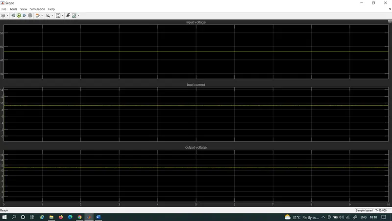
Conclusion:The buck converter is designed and simulated in simulink gave 48 V dc input and got 12V dc output.