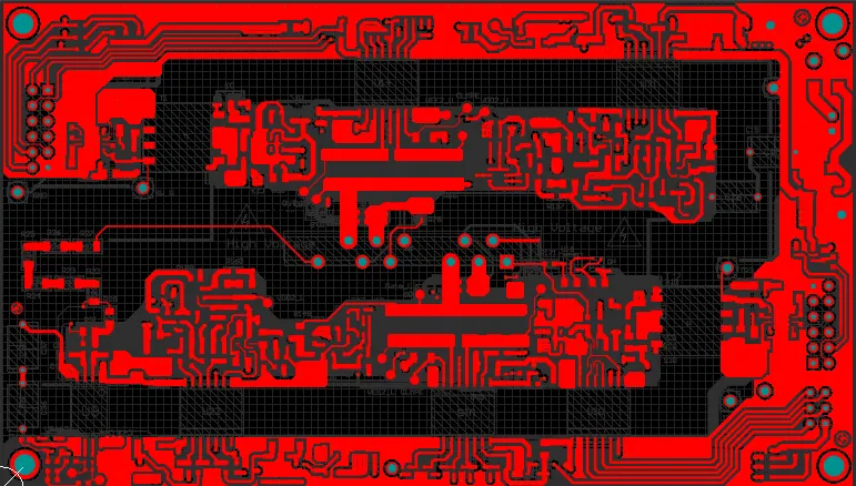
Project 2 - SiC/IGBT isolated gate driver reference design with thermal diode and sensing FET
1.How will you decide the layer stack up.
Factors that need to be considered are
- Multi-layers with an even number of layers.
- Maintain a symmetrical stack up with a copper balance
- Balance Power and Ground layers in relation to the center of the board.
- Determine if a core construction or foil construction should be used.
Reason for using even the number of layers: In the multilayer PCB fabrication process, at a high temperature and pressure, layers are pressed together for long hours. In an odd-layered PCB, due to the standard symmetrical requirement, the outer copper core requires additional processing, which increases the risk of scratches and etch errors on the outer layers and also creates uneven weight during the copper plating stage and results in irregular plating issues. Processing odd number layer PCB is costlier than even number layer PCB. Odd-layered circuit boards are easy to get bent. When the multilayer printed circuit board is cooling after the lamination bonding process, the different lamination tensions might cause the PCB to bend. As the thickness of the multilayer printed circuit board increases, the bending risk of a composite PCB with two different structures increases.
Symmetrical stack-up with copper balancing to reduce bow and twist: The key to eliminating board bending is to employ a balanced stack-up. Although a few degrees of bending are allowed, the subsequent processing efficiency will decrease, resulting in an increase in total cost. The elements like traces, core, layers and final coating consist of copper as the main component. If copper coverage is inconsistent between the layer stack-up, it can lead to issues like bows and twists, etc. PCB Bow and Twist are parameters that determine alignment errors in a PCB board based on its flatness. A board with a bow issue will lift off the surface despite all corners of the board making contact with the plane. The twist occurs when three of the PCB corners are in contact with the surface while the fourth corner is elevated.
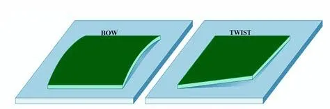
According to the IPC-A-600 standard, boards with less than 1.5% of bow and twist are acceptable. In the case of the boards with SMD components, this percentage needs to be less than 0.75%.
PCB Bow and Twist can be used by a number of factors that include high-temperature exposure, heavy thermal shocks during soldering, etc. The board design, thickness, layers, and materials also play a role in the board showing Bows and Twists over various fabrication, assembly, or operating conditions.
Balance Power and Ground layers in relation to the center of the board: For multilayer PCBs, general layers include the ground plane (GND plane), power plane (PWR plane), and inner signal layers. Here's a sample of an 8-layer PCB stackup.
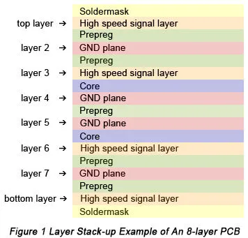
core construction and foil construction: In the core structure, all conductive layers in the circuit board are coated on the core material; in the foil-clad structure, only the inner conductive layer of the circuit board is coated on the core material, and the outer conductive layer is a foil-clad dielectric board. All conductive layers are bonded together through a dielectric using a multilayer lamination process.
2. How do you calculate the trace width, via size and trace length?
There is software that can calculate the trace width, via size and trace length.
There are a few things to know before calculating trace width, via size and trace length is followed by
- The IPC-2221 data from which these formulas are derived only covers up to 35 Amps, trace width up to 400 mils, allowable temperature rise from 10 to 100 degrees Celsius, and copper of 0.5 to 3 ounces per square foot. If used outside of these ranges, this calculator will extrapolate thus becoming more inaccurate with higher currents.
- External layers have better heat transfer than internal layers as air dissipates heat due to convection, while the internal dielectric does not conduct heat as well. Since the goal of the Trace Width Calculator is to prevent an excessive temperature rise of the traces, it makes the internal traces wider because they store more heat. In the case of a circuit in a vacuum, or in a potted assembly, external layers do not have the benefit of heat convection in the air thus you should use the internal trace width for all traces.
- Temperature rise is the difference between the maximum safe operating temperature of your PCB material and the typical operating temperature of your board.
- Higher current flow increases the temperature of the copper traces therefore, the temperature rise is a design parameter for how much added heat you would like to design for. Based on this limit the formula chooses a width to stay within it. Ten degrees is a safe rule of thumb for most applications. If you need to reduce trace width then you can increase this value if your PCB material and operating temperature allow.
- A Mil is one thousandth (1/1000) of an inch or 0.0254mm. Its name is derived from the Latin mille meaning thousand. In electronics, mil is commonly used but in other disciplines, it may be referred to as thou and a mil being a millimeter
Bittele electronics' calculator is used here to calculate the trace width, via size and trace length.
The input data is taken from the Description as current maximum 180ma, Peak Voltage 65V, and other details Cu thickness 1oz/ft^2, Temperature rise 10 degrees celsius, Ambient Temperature is 25-degree celsius, and Conductor Length is 1 inch
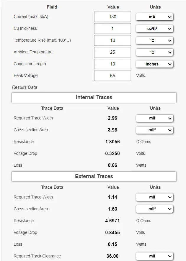
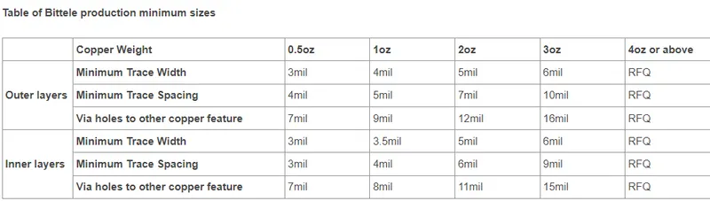
for 1oz copper weight in an outer layer need Minimum trace width of 4mil, Minimum trace spacing of 5mil, and Via holes of 9mil
1oz copper weight in an inner layer needs Minimum trace width of 3.5mil, Minimum trace spacing of 4mil, and Via holes of 8mil are shown in the calculator.
3. What do you do to avoid heating components in a 4-layer PCB?
A PCB is basically a heat-generating factory because of all the heat-producing components it contains. The PCB needs some way to dissipate all that thermal energy.
PCB heat dissipation techniques:
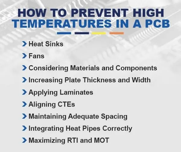
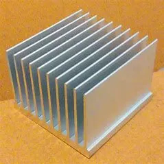
1. Heat sinks
Heat sinks is a passive heat exchanger that transfers the heat generated by an electronic or a mechanical device to a fluid medium, often air or a liquid coolant, where it is dissipated away from the device
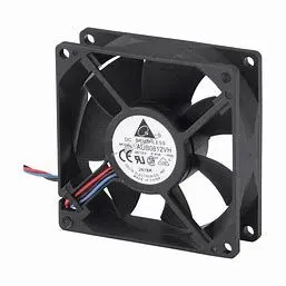
2. Cooling Fan
Most electronic devices contain fans for cooling, and part of the purpose of those fans is to help cool PCBs. Cooling fans disperse heat out of electronic devices while letting cool air in, helping to prevent overheating and extend the PCB’s lifespan and performance.
3. Considering materials and components
Choosing heat-resistant materials is one of the most effective strategies for reducing heat in a PCB. For example, heavy copper PCBs constructed with thick copper plates make excellent choices for their durability and ability to withstand high temperatures. They handle higher levels of currents, resist higher temperatures for longer amounts of time, and provide stronger connection points than standard PCBs. For these reasons, they are particularly useful in automotive, aviation, heavy machinery and power converter applications, and other heavy-duty environments.
Materials such as RF materials — used in radio-frequency circuits — and polyamide are also sensitive to high temperatures. Polytetrafluoroethylene (PTFE) is extremely common in RF boards, but it can smear under the heat of drilling, and the smear is very difficult to remove. Making use of a high-temperature laminate in these situations is highly recommended.
4. Increasing plate thickness and width
In PCBs, thicker plates tend to conduct heat less effectively than thinner ones. They require more power to reach high temperatures, so this can help reduce the risk of overheating, warping, and disruption.
5. Applying laminates is another way to prevent damage from high temperatures. High-temperature PCB laminates can prevent overheating by offering heat protection for the PCB’s components.
High-temperature laminates should have the following protective properties:
- Glass transition temperature (TG): Glass transition temperature refers to the temperature at which polymers shift thermodynamically from rigid to soft. High_TG PCBs offer superior protection.
- Time to delamination: High heat can delaminate a PCB laminate over time. The best laminates will take a long time to become delaminated at high temperatures.
- Moisture absorption: PCB laminates should have dependable, protective moisture-absorption capabilities. If the PCB will operate in an air-controlled environment like a laboratory, moisture absorption may not be a high priority. But if the PCB will operate in an environment where it may become exposed to the elements, adequate moisture-absorption capabilities are critical.
- Decomposition temperature (TD): Decomposition temperature refers to the temperature at which 5% of the laminate’s mass is lost because of decomposition. A high decomposition temperature offers superior protection.
- Z-axis expansion: Z-axis expansion refers to the expansion of the material along the z-axis as a percentage of the coefficient of thermal expansion. Lower z-axis expansion also offers superior protection.
6. Aligning CTEs
The coefficient of thermal expansion (CTE) measures how much a material expands when exposed to high temperatures. In PCB design, it’s ideal for the dielectric layers to have a similar CTE to that of the copper layers. That way, if the layers expand, they do so in a uniform way that leads to minimal damage.
In a multilayer stack, if CTEs are not aligned, the layers will expand at radically different rates, which can cause warping and disruption. If this uneven expansion occurs during PCB assembly, the misalignments can also cause serious problems for drilling.
Choosing PCB materials with lower CTEs helps prevent overheating. For example, PTFE filled with woven glass or microglass fibers has excellent electrical characteristics, but it also has a high CTE. So this material is a poor choice when thermal toughness is a top priority. On the other hand, PTFE filled with ceramic has a lower CTE and performs much better at high temperatures, though it loses a little in electrical characteristics.
7. Maintaining adequate spacing
Determining component spacing on a PCB can be a tricky process. When board components are too close together, crosstalk may result — that is, different components may begin interacting with each other in undesirable ways. These unwanted interactions lead to something known as the skin effect. When the skin effect occurs, trace resistances increase, leading to resistive losses and adding heat to the circuit. The skin effect is particularly common with high-frequency PCBs, so there must take extra care with component spacing to keep the boards from overheating.
8. Integrating Heat Pipes
Heat pipes in a PCB can help disperse heat as well. The liquid in the pipes can absorb heat and prevent it from damaging the components of the board.
9. Maximizing RTI and MOT
Relative thermal index (RTI) and maximum operating temperature (MOT) are two relevant measurements we should pay careful attention to in the design of PCBs.
RTI indicates the highest temperature that a material can handle without undergoing changes to its properties or a reduction in its performance. MOT refers to the highest temperature that a particular circuit board configuration can withstand without undergoing changes to its properties or diminution of its performance. Engineers should keep both these measurements in mind in the design of PCBs and choose materials and circuit components with robust heat resistance as determined by these metrics.
4. Advantages of multilayer PCB:
The significant multilayer PCB benefits include:
1. High Quality
A significant increase in functionality with the incorporation of multiple layers. Multilayer boards result in high-quality, reliable products.
2. Increase Space for additional component
With the extra layers what opens up is added real estate. Signal and power traces can be shifted to the internal layers where there is space for direct connections. What it also does is free space on the board’s external layers for additional components.
3. Improves Electrical Performance
On account of their innate electrical properties, they offer high capacity and speed. They also solve electrical performance issues such as:
a. EMI Shielding
It is possible to configure the layer structure so that multiple ground planes are included. In turn, these ground planes act as a shield against electromagnetic interference.
b. Signal integrity
It is possible to configure multilayered boards with microstrip and to sandwich high-speed transmission lines. In turn, these ensure better signal paths and also reduce noise.
c. Power integrity
With full metal power and ground planes power is distributed well. Besides, the planes also absorb any power spikes.
d. Thermal control
Multilayered boards ensure heat dissipation throughout the board layer stack up.
4. Reduce overall weight and connectors
They significantly reduce the need for multiple connectors. Not only does this result in simplifying construction, but importantly, it also results in reducing its weight.
5. Multilayer PCBs also lend themselves to both rigid and flexible boards.
6. The high density also results in increased durability.
PCB layout is taken from texas instruments and PDF is attached below.