Project 1 - Loss calculation for a DC/DC converter-MATLAB
| PROJECT 1 - Loss Calculation for DC/DC Converter |
AIM : Design a Boost Converter, Calculate loss of different components and derive efficiency of the same.
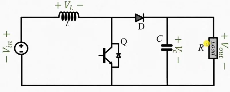
THEORY : A boost converter Step Ups or Boost the output voltage when connected across a specifed DC voltage source.
Diagram below shows circuit diagram of Boost Converter :-
 |
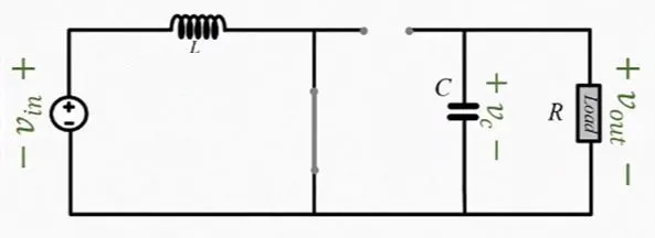
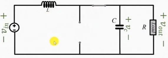
Operation :-
| ON Mode | OFF Mode | ||
|
|
||
|
|
Parameters Considered:-
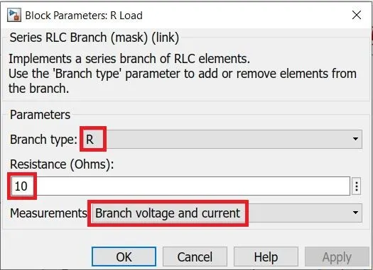
`V_(i\n) = 100\ \V;\ \V_(out) = 200\ \V; R_(load) = 10\ \Omega; f_(sw) = 10\ \kHz`
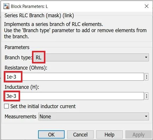
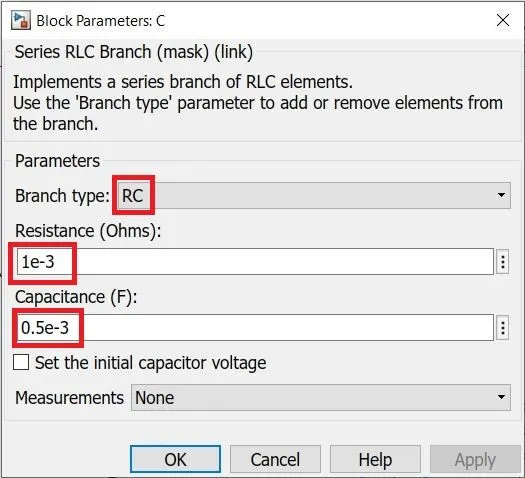
`R_(L) = 1\ \mOmega;\ \R_(C) = 1\ \mOmega`
Duty Cycle -
| `V_(out)/V_(i\n) = 1/(1-D)` |
`200/100 = 1/(1-D)`
`D = 0.5`
Inductor Design -
| `L > (V_(i\n)*D)/(f_s*DeltaI_L)` |
`I_L = V_o/R = 200/10 = 20\ \A`
`DeltaI_L = 10%\ \of\ \I_L = 2\ \A`
`L > (100*0.5)/(10000*2)`
`L > 2.5\ \mH`
Capacitor Design -
| `C_(out) = (D)/(R*f_s*(DeltaV_o)/V_o)` |
`(DeltaV_o)/V_o = 0.01`
`C_(out) = (0.5)/(10*10000*0.01)`
`C_(out) = 0.5\ \mF`
SIMULINK MODEL
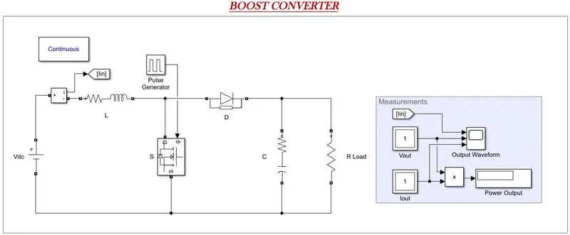 |
Following blocks have been used to make the model -
| 1. | DC Voltage Source : It is set at 100 V. | |||
|
2. |
Series RLC Branch : It is used to model Inductor, Capacitor and Resistive load.
|
|||
|
3. |
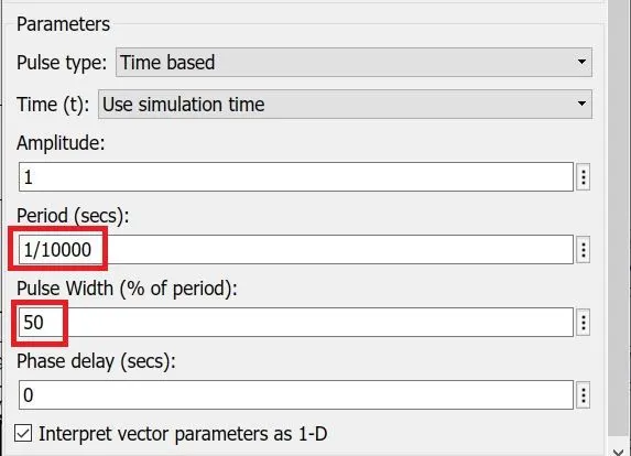
Pulse Generator : It is used to generate gate pulses for the MOSFET. Switching Frequency is 10 kHz.
|
|||
|
4. |
Measurements : Multimeter is used to take measurements from the Load Resistor. The same has been connected across a Scope and a Display block. Input current is also connected across the same scope using a Current Measurement Block. |
OBSERVATIONS :
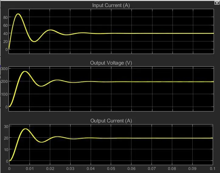
The simulation is run for 0.1 seconds and output is evaluated across the scope.
| Normal Scope | Zoomed Scope |
 |
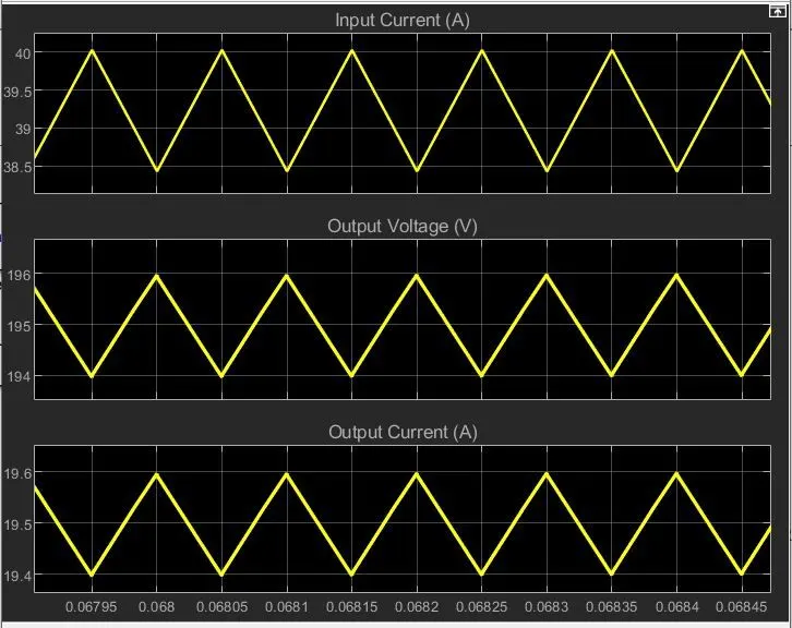 |
- Input Current = ~ 39.5 A.
- Output Voltage = 195 V. Showing the boosted voltage.
- Output Current = 19.5 A.
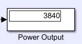
Output Power -
|
Calculated Output `P_(out) = V_(out)*I_(out)` `P_(out) = 200*20` `P_(out) = 4000\ \W` |
Simulated Output
|
CALCULATIONS :
Power Loss in Boost Converter is given by :-
`P_(Loss) = P_(mos\fet)\ \+\ \P_(diode)\ \+\ \P_(i\nduct\o\r)\ \+\ \P_(c\apacit\o\r)`
1. Mosfet Loss / Conduction Loss.
| `P_(cond) = I_(i\n)^2*R_(DsON)*D` |
`R_(DsON)` is taken from 'NCE0240' Mosfet Datasheet from NC power. (PFA)
`P_(cond) = (40)^2*(0.041)*(0.5)`
`P_(cond) = 32.8\ \W`
2. Diode Loss.
| `P_(d) = V_(f)*I_(i\n)*(1-D)` |
`V_f` is taken from 'V40PW22C' Diode Datasheet from Vishay Semiconductor. (PFA)
`P_d = (0.58)*(40)*(0.5)`
`P_d = 11.6\ \W`
3. Inductor Loss.
| `P_(L) = (I_(i\n)^2*R_(L))\ \+\ \(R_(L)/12)((D*V_(i\n))/(f_s*L))` |
`P_(L) = (40^2*0.001)\ \+\ \(0.001/12)((0.5*100)/(10000*0.0025))`
`P_(L) = 1.6\ \W`
4. Capacitor Loss.
| `P_(C) = R_(C)*D*(1-D)*I_(i\n)^2\ \+\ \(R_C/12)*(1-D)*((D*V_(i\n))/(f_s*C))` |
`P_(C) = (0.002*0.5*0.5*40^2)\ \+\ \(0.002/12)*(0.5)*((0.5*100)/(10000*0.005))`
`P_(C) = 0.8\ \W`
5. Efficiency.
Total Loss = Conduction Losses + Diode Losses + Inductor Loss + Capacitor Loss
`P_(Loss) = P_(mos\fet)\ \+\ \P_(diode)\ \+\ \P_(i\nduct\o\r)\ \+\ \P_(c\apacit\o\r)`
`P_(Loss) = 32.8\ \+\ \11.6\ \+\ \1.6\ \+\ \0.8`
`P_(Loss) = 46.8\ \W`
`P_(out) = P_(i\n)\ \-\ \P_(loss)`
`P_(out) = 4000 - 46.8`
`P_(out) = 3953.2\ \W`
| Caculated Efficiency | Simulated Efficiency |
|
`eta = P_(out)/P_(i\n)` `eta = 3953.2/4000` `eta = 0.9891\ \=\ \98.83%` |
`eta = P_(out)/P_(i\n)` `eta = 3840/4000` eta = 0.96\ \=\ \96% |
CONCLUSION :
The designed Boost Converter model is successfully simulated along with power loss calculation.
The deviation in calculated efficiency and simulated efficiency is due to the real time simulation environment of MATLAB.
Efficiency of the designed Boost converter comes out to be 95 - 99%.
Bibliography :
https://www.tib-op.org/ojs/index.php/th-wildau-ensp/article/view/8/175