Project 1 - 40-V to 80-V adjustable output voltage boost reference design for LIDAR applications
1.How will you decide the layer stack up.
Factors need to be consider are
- Multi-layers with an even number of layers.
- Maintain a symmetrical stack up with copper balance
- Balance Power and Ground layers in relation to the center of the board.
- Determine if a core construction or foil construction should be used.
Reason for using even the number of layers: In the multilayer PCB fabrication process, at a high temperature and pressure, layers are pressed together for long hours. In an odd-layered PCB, due to the standard symmetrical requirement, the outer copper core requires additional processing, which increases the risk of scratches and etch errors on the outer layers and also creates uneven weight during the copper plating stage and results in irregular plating issues. Processing odd number layer PCB is costlier than even number layer PCB. Odd-layered circuit boards are easy to get bent. When the multilayer printed circuit board is cooling after the lamination bonding process, the different lamination tensions might cause the PCB to bend. As the thickness of the multilayer printed circuit board increases, the bending risk of a composite PCB with two different structures increases.
Symmetrical stack-up with copper balancing to reduce bow and twist: The key to eliminating board bending is to employ a balanced stack-up. Although a few degrees of bending are allowed, the subsequent processing efficiency will decrease, resulting in an increase in total cost. The elements like traces, core, layers and final coating consist of copper as the main component. If copper coverage is inconsistent between the layer stack-up, it can lead to issues like bows and twists, etc. PCB Bow and Twist are parameters that determine alignment errors in a PCB board based on its flatness. A board with a bow issue will lift off the surface despite all corners of the board making contact with the plane. The twist occurs when three of the PCB corners are in contact with the surface while the fourth corner is elevated.
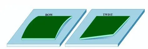
According to the IPC-A-600 standard, boards with less than 1.5% of bow and twist are acceptable. In the case of the boards with SMD components, this percentage needs to be less than 0.75%.
PCB Bow and Twist can be used by a number of factors that include high-temperature exposure, heavy thermal shocks during soldering, etc. The board design, thickness, layers, and materials also play a role in the board showing Bows and Twists over various fabrication, assembly, or operating conditions.
Balance Power and Ground layers in relation to the center of the board: For multilayer PCBs, general layers include the ground plane (GND plane), power plane (PWR plane), and inner signal layers. Here's a sample of an 8-layer PCB stackup.
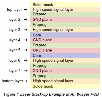
core construction and foil construction: In the core structure, all conductive layers in the circuit board are coated on the core material; in the foil-clad structure, only the inner conductive layer of the circuit board is coated on the core material, and the outer conductive layer is a foil-clad dielectric board. All conductive layers are bonded together through a dielectric using a multilayer lamination process.
2. How do you calculate the trace width, via size and trace length?
There is software that can calculate the trace width, via size and trace length.
There are a few things to know before calculating trace width, via size and trace length is followed by
- The IPC-2221 data from which these formulas are derived only covers up to 35 Amps, trace width up to 400 mils, allowable temperature rise from 10 to 100 degrees Celsius, and copper of 0.5 to 3 ounces per square foot. If used outside of these ranges, this calculator will extrapolate thus becoming more inaccurate with higher currents.
- External layers have better heat transfer than internal layers as air dissipates heat due to convection, while the internal dielectric does not conduct heat as well. Since the goal of the Trace Width Calculator is to prevent an excessive temperature rise of the traces, it makes the internal traces wider because they store more heat. In the case of a circuit in a vacuum, or in a potted assembly, external layers do not have the benefit of heat convection in the air thus you should use the internal trace width for all traces.
- Temperature rise is the difference between the maximum safe operating temperature of your PCB material and the typical operating temperature of your board.
- Higher current flow increases the temperature of the copper traces therefore, the temperature rise is a design parameter for how much added heat you would like to design for. Based on this limit the formula chooses a width to stay within it. Ten degrees is a safe rule of thumb for most applications. If you need to reduce trace width then you can increase this value if your PCB material and operating temperature allow.
- A Mil is one thousandth (1/1000) of an inch or 0.0254mm. Its name is derived from the Latin mille meaning thousand. In electronics, mil is commonly used but in other disciplines, it may be referred to as thou and a mil being a millimeter
Bittele electronics' calculator is used here to calculate the trace width, via size and trace length.
The input data is taken from the Description as current maximum 100ma, Peak Voltage 80V, and other details Cu thickness 1oz/ft^2, Temperature rise 10 degrees celsius, Ambient Temperature is 25-degree celsius, and Conductor Length is 1 inch
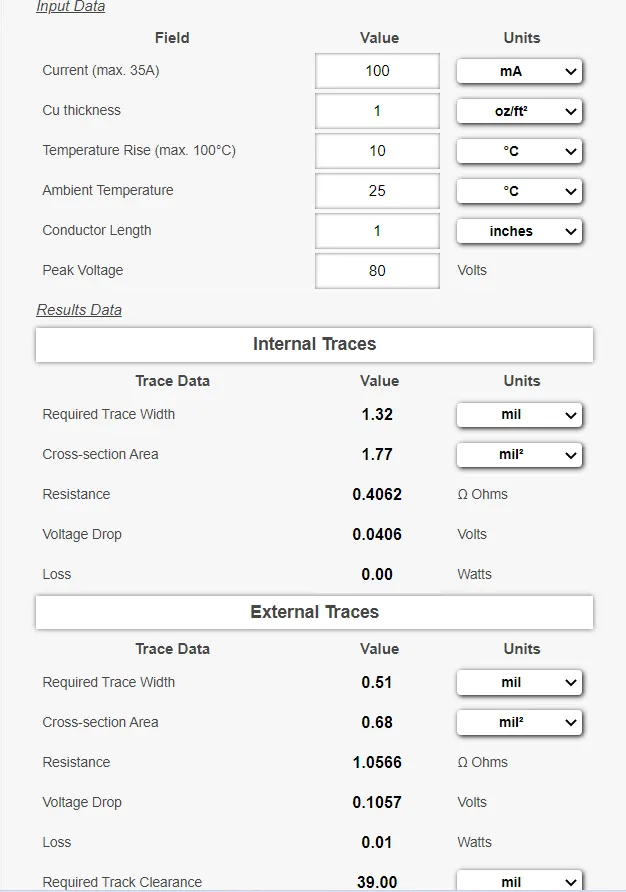
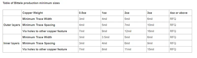
for 1oz copper weight in an outer layer need Minimum trace width of 4mil, Minimum trace spacing of 5mil, and Via holes of 9mil
for 1oz copper weight in an inner layer need Minimum trace width of 3.5mil, Minimum trace spacing of 4mil, and Via holes of 8mil are shown in the calculator.
3. What is the drawback of having 2 layers of PCB?
The main drawback of 2 Layer PCBs is that they are not as durable as other types of PCBs. In other words, 2 Layer PCBs are also more susceptible to crosstalk and noise than other types of PCBs.
In short, the disadvantages of double-sided PCB include higher prices, longer manufacturing processes, more difficulty to solder, and lower yield rate.
The benefits of multilayer PCBs are numerous, making them applicable to a wide variety of advanced technologies. However, these types of PCBs aren't appropriate for all applications. In fact, several drawbacks can outweigh multilayer PCB advantages, especially for electronics of lower cost and complexity. These disadvantages include the following:
· Higher Cost: Multilayer PCBs are significantly more expensive than single and double-layer PCBs at every stage of the manufacturing process. They are difficult to design, taking an extensive amount of time to work out any potential problems. They also require a highly complex manufacturing process to produce, which takes a great deal of time and labor on the part of assembly personnel. Additionally, due to the nature of these PCBs, any mistake in the manufacturing or assembly process is prohibitively difficult to rework, resulting in either additional labor costs or scrap material expenses. On top of it all, the equipment used to produce multilayer PCBs is quite expensive because it is still a relatively new technology. For all those reasons, unless a small size is an absolute necessity for the application, cheaper alternatives may be a better choice overall.
· Complicated Production: Multilayer PCBs are more difficult to produce, requiring much more design time and careful manufacturing techniques than other PCB types. This is because even small flaws in the PCB's design or manufacture could render it useless.
· Limited Availability: One of the largest issues with multilayer PCBs is the expenses of the machinery needed to produce them. Not all PCB manufacturers have the funds or the necessity for this machinery, so not all PCB manufacturers carry it. This limits the number of PCB manufacturers available to produce multilayer PCBs for clients. Thus, it's best to carefully inquire a PCB manufacturer's capability in terms of multilayer PCBs prior to deciding it as your contract manufacturer.
· Skilled Designer Required: As previously discussed, multilayer PCBs require extensive design beforehand. Without previous experience, this can be problematic. Multilayer boards require interconnection between layers, but must simultaneously mitigate crosstalk and impedance issues. A single problem in the design can result in a non-functioning board.
· Production Time: With increased complexity comes more manufacturing requirements. This plays into a key issue with multilayer PCBs' turnover rate - each board requires a significant amount of time to produce, resulting in more labor costs. Additionally, it possibly leads to longer periods between when an order is placed and when the product is received, which can be a problem in some circumstances.