Project 1
Project 1
Design and Simulation of Power converters
Aim:
To design and simulate the power converters using given requirements in Simulink and analyze and justify the plots.
Software used:
MATLAB/ Simulink
Considered Converters:
- Buck converter in CCM (continuous conduction mode)
- Buck Converter in DCM (Discontinuous conduction mode)
- Boost Converter in CCM (Continuous conduction mode)
Buck Converter in CCM:
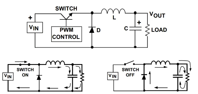
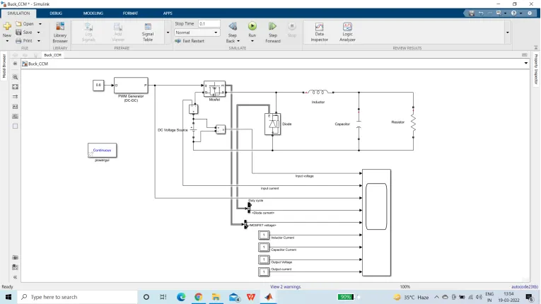
DC- DC Buck converter is used to reduce the voltage from the high level to low level. It is most commonly used in electric vehicles to reduce the voltage from the 48V battery system to 12V system which is used for the vehicle accessory loads such as radio, speaker, horn, charging port, etc. It is an application of switched mode power converters. It has high efficiency and less loss. It requires controlled gate supply. It consists of MOSFET, inductor, capacitor, diode and resistor load.
Operation:
If the supply voltage is directly connected to the load through the MOSFET which acts as switch, whenever the switch is ON the input voltage is directly connected to the load and MOSFET acts as short circuit. When the switch is OFF the input is isolated from the load and the MOSFET acts as open circuit. When the duty cycle is given as according to the required output, the Buck converter produces the oscillating output. But the average output is same as required output.
In order to reduce the oscillations, the capacitor is connected in parallel to maintain the voltage across the load when the switch is in OFF condition. But when the switch is ON, the high inrush current flows through the capacitor when connected in parallel across the source. This may damage the components and system.
In order to reduce this high inrush current, inductor is connected in series because inductor does not allow the sudden rise in current. And also another problem arises when switch is off. The inductor does not have any closed path to discharge the current stored in the inductor. Hence the diode is connected in parallel to the inductor. Hence it all combined to form the final model of the Buck converter. The operation is visualized in the below circuit diagram.
Model:
Explanation:
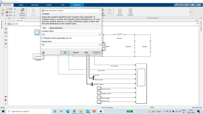
- Given that Input voltage is 50V and required Output voltage is 30V and output power is 500W.
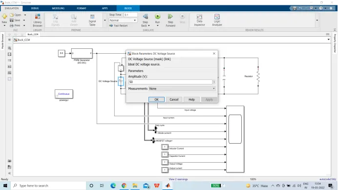
- So, duty cycle D = Vout/Vin
= 30/50
D = 0.6
Let us consider, the switching frequency = 100kHz.
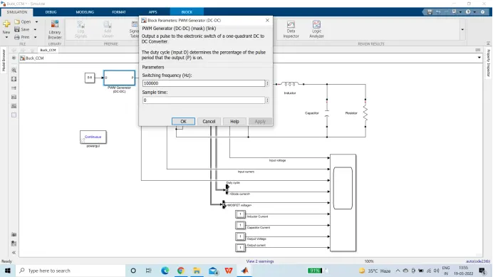
- The inductor current is equal to the sum of capacitor current and load current.
- The average current of the capacitor is 0. Hence the inductor current is equal to load current.
- So the current through the inductor I(L) = IR = P/V = 500/30 =16.6667A
- Load Resistor R = V/I = 30/16.6667 = 1.7999 ohm.
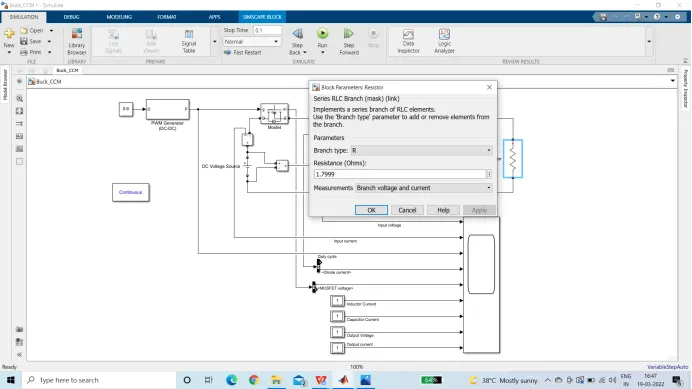
- And according to given condition, the current has to be continuous.
- For the continuous current, the value of inductor is,
L = (Vout*(1-D))/(fs*del(I))
fs = switching frequency.
del(I) = Ripple current.
Ripple current must be less than 30%. Let us consider as 10%.
del(I) = 16.6667*0.1 = 1.66667
L = (30*0.4) / (100*10^3*1.66667)
L = 71.9985uH
Let us consider the inductor value as 71.9985uH.
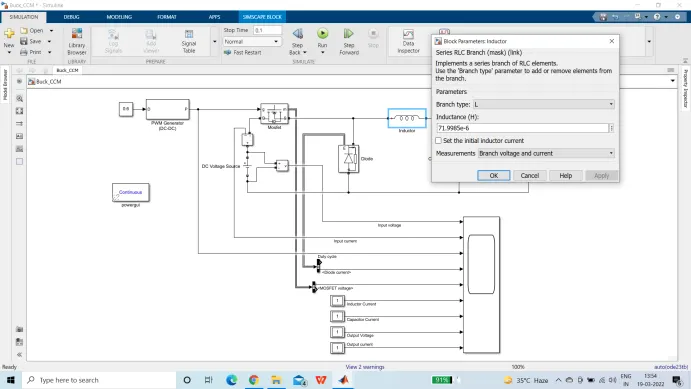
- The value of capacitor is obtained by using the formula,
C = (1-D)/(8*L*fs^2*(del(Vout)/Vout))
Ripple voltage must be less than 5%. Let us consider 1%.
C = 0.4 / (8*71.9985*10^-6 * (100*10^3)^2 * 0.01)
C = 6.944uF
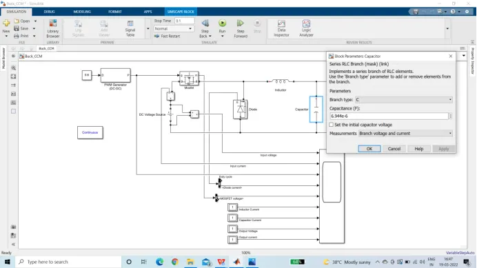
- Configure the above value in the model and run the simulation for 100ms.
Plots:
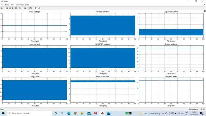
Zoomed Out View:
Zoomed In View:
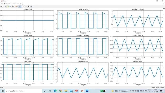
Summary:
From the above plot, it is visualized that when the switch is ON, we observe increasing output current. When the switch is in OFF condition the MOSFET current becomes zero, but the output current is does not becomes zero it slowly reducing due to the current stored in the inductor passes through the diode to complete the circuit. Hence the current increases when the switch is ON and current decreases when switch is OFF. It is also observed that the current through the inductor is continuous and is not falling to zero. Hence this is called as Buck converter in Continuous Conduction Mode (CCM).
From the above plot it is observed that the output voltage is varying between 29.65V to 29.85V. The ripple is 0.3V which is 1% that we considered. The average output voltage is 29.7V. And the output current is varying between 16.42A to 16.58A. The average output current is 16.5A. The small deviation from the calculated values is due to switching loss.
Thus the voltage is reduced from 50V to 29.85V and the current in the inductor is continuous. Hence it is Buck converter in CCM mode designed and simulated.
Buck Converter DCM(Discontinuous conduction mode):
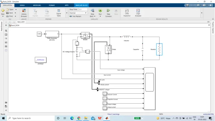
Here in order to reduce the cost of converter discontinuous conduction mode is used. The increase in cost of converter in CCM mode is due to the size of the inductor used. That size of the inductor is reduced in the DCM to attain the required output. All other operation are same as per the buck converter in discontinuous conduction mode. The difference in the operation during the OFF time of the switch, the energy stored in the conductor is discharged through the load and diode. But this stored energy is not enough to supply the load for the whole duration of OFF time. Hence there is no current through the inductor for some duration of time. So this mode of operation is called Discontinuous conduction mode.
Model:
Procedure:
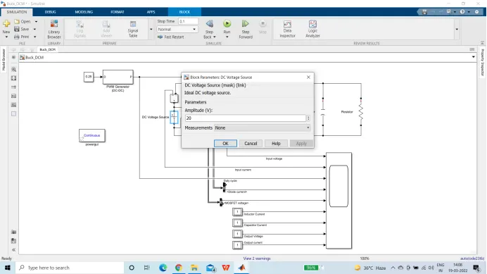
- Given that Input voltage is 20V and required Output voltage is 5V and output power is 100W.
- So, duty cycle D = Vout/Vin
= 5/20
D = 0.25
Let us consider, the switching frequency = 100kHz.
- The inductor current is equal to the sum of capacitor current and load current.
- The average current of the capacitor is 0. Hence the inductor current is equal to load current.
- So the current through the inductor I(L) = IR = P/V = 100/5 =20A
- Load Resistor R = V/I = 5/20 = 0.25 ohm.
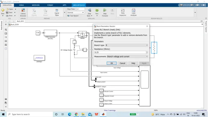
- And according to given condition, the current has to be dis
- For the continuous current, the value of inductor is,
L > ((1-D)*R)/(2*fs)
fs = switching frequency.
L > (0.75*0.25) / (2*100*10^3)
L > 0.9375uH
For Discontinuous current,
Hence let us consider L = 0.85uH
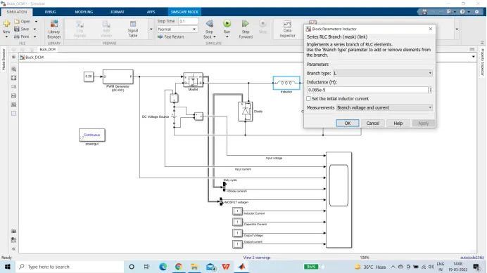
New Duty ratio for Discontinuous conduction mode,
Vo/Vin = D/(D+D1).
Vo/Vin = 2D/(D+sqrt(D^2+8L/RT))
5/20 = 2D/(D + sqrt(D^2 + ((8*0.85*10^-6)/(0.25*1/10^5)))
0.25 = 2D/(D + sqrt(D^2 + 2.72))
D + sqrt(D^2 + 2.72) = 2D/0.25
sqrt(D^ + 2.72) = 7D
D^2 + 2.72 = 49 D^2
D^2 = 2.72/ 48
D^2 = 0.056667
D = 0.238
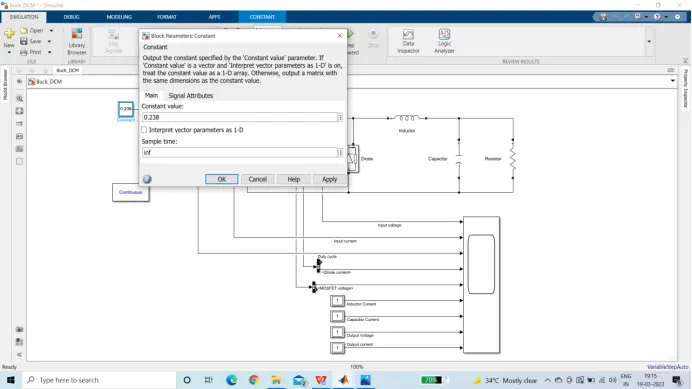
Therefore, Vo/Vin = D/(D+D1)
5/20 = 0.238/(0.238+D1)
D1 = 0.714
(1-D) = 0.762
Hence D1 < (1-D).
The condition for discontinuous conduction mode, D1 < (1-D) is satisfied.
- The value of capacitor is obtained by using the formula,
C = (1-D)/(8*L*fs^2*(del(Vout)/Vout))
Ripple voltage must be less than 5%. Let us consider 1%.
C = 0.762 / (8*0.85*10^-6 * (100*10^3)^2 * 0.01)
C = 1.1205mF
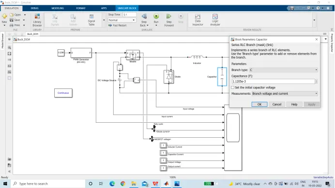
- Configure the above value in the model and run the simulation for 100ms.
Plots:
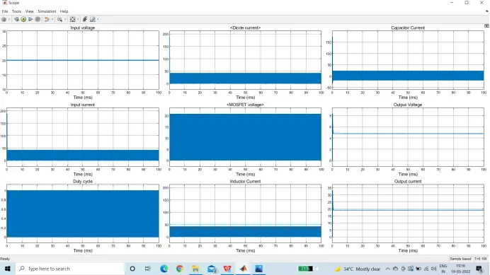
Zoomed Out View:
Zoomed In View:
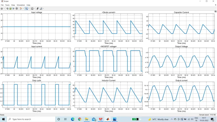
Summary:
From the above plots, it is observed that the inductor current is discontinuous. During the ON time of the switch, the inductor stores the energy, capacitor gets charged and load is supplied. During the OFF time of the switch, the energy stored in the inductor supplies the load and complete the circuit through freewheeling diode and capacitor also supports load. Since the inductor size is small it can’t feed the supply during the entire period OFF state of switch, the inductor discharged completely. This clearly observed in the above plot. But the load has to be fed, hence that is fed by capacitor. This can seen in the plot, the negative value of capacitor current represents the capacitor is discharging.
From the above plot it is observed that, the output voltage is varying between 4.74V to 4.79V. The average output voltage is 4.765V. The output current is varying between 18.95A to 19.15A. The small deviation between obtained value and calculated value is due to switching resistance.
Thus the voltage is reduced from 20V to 4.79V and the current in the inductor is discontinuous. Hence it is Buck converter in DCM mode designed and simulated.
Boost Converter CCM (Continuous Conduction Mode):
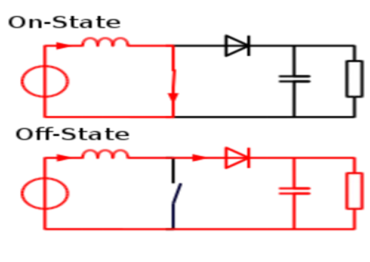
DC-DC boost converter is usually used to increase the voltage level. When the MOSFET is ON the voltage source is short circuited through the switching inductor. The voltage across the inductor is input voltage. By this time the load is fed by the charge stored in the capacitor. When the MOSFET is OFF, the input is connected to load through the inductor and diode as it is forward biased. Since the current through the inductor is same energy stored in the inductor also acts as another source in addition the voltage source, the output voltage is higher than input. Since voltage gets boosted. During this time, the capacitor gets charged.

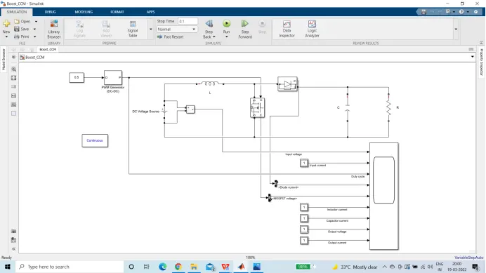
Model:
Procedure:
- Given that Input voltage is 20V and required Output voltage is 40V and output power is 600W.
Duty cycle:
Ideal duty cycle D:
Vout/Vin = 1/(1-D)
1-D = Vin/Vout = 20/40
D = 0.5
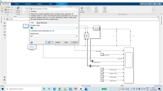
Let us consider the switching frequency as 100kHz.
Resistor:
Power extracted is 30W
P = Vo*R = 18^2/30
IR = 600/40
IR = 15A
IL = IR/(1-D) = 15/0.5
IL = 30A
R = V/IR = 40/15
R = 2.6667 ohm
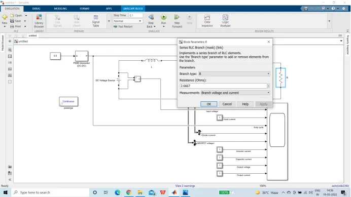
- For the continuous current, the value of inductor is,
L = (Vin*D)/(fs*del(IL))
fs = switching frequency.
del(IL) = Ripple current.
Ripple current must be less than 30%. Let us consider as 10%.
del(IL) = 30*0.1 = 3A
L = (20*0.5) / (3*100*10^3)
L = 3.333*10^-5 H
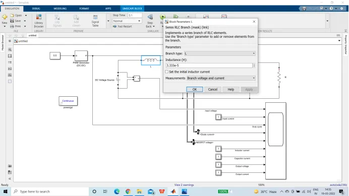
- The value of capacitor is obtained by using the formula,
C = (D)/(R*fs*(del(Vout)/Vout))
Ripple voltage must be less than 5%. Let us consider 1%.
C = 0.5 / (2.6667 * 100*10^3 * 0.01)
C = 0.1874mF
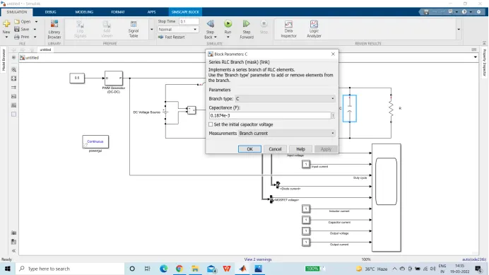
- Configure the above value in the model and run the simulation for 100ms.
Plots:
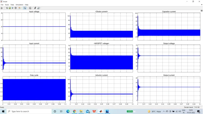
Zoomed Out View:
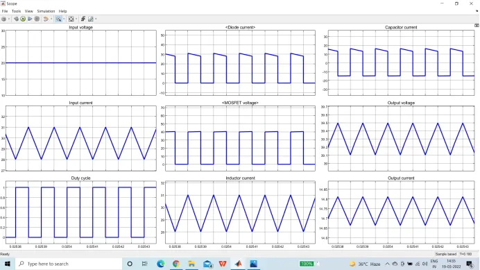
Zoomed In View:
Summary:
From the above plot, it is observed that when the MOSFET is ON the current through the inductor increases as the circuit is short circuited and gets charged. During this output current decreases and this current is fed by capacitor and is observed as negative value. When the MOSFET is OFF, the current flows through inductor, diode and load. During this time, the output load is fed by source and inductor hence the output voltage and current increases. During this time, inductor gets discharged and the inductor current is reducing and capacitor gets charged so, capacitor current increases.
From the above plot it is observed that, the output voltage is varying between 39.1V to 39.5V and the ripple is 1%. The average output voltage is 39.3V. The output current is varying between 14.67A to 14.82A. The average output current is 14.74A. The small deviation between the calculated value and observed value is due to small switching loss.
The voltage is boosted from 20V to 39.5V and current through the inductor is also continuous. Hence it is Boost converter is DCM is designed and simulated.
Result:
Hence the converters with the required specification are designed and simulated. The result plots are attached and justified with explanations.