Duty cycle control signal generated for a simple power converter circuit using buck converter MATLAB model.
Objective
> Efficiency and losses of power electronic circuits
> Using buck converter MATLAB model, show how duty cycle control signal can be generated for a simple power converter circuit
> Comparison of square wave inverter output voltage with sine modulated one.
> Difference between VFD and Vector control drive.
Efficiency and losses of power electronic circuits
Power electronics
> Power electronics plays an important role in our today society. It is present almost all power supplies, in servo systems and variable drives.
> Power electronics deals with the conversion and control of electrical energy with the help of power semiconductor devices that operate in a switching mode therefore, efficiency of power electronic apparatus may approach as high as 98–99%.
> This technology uses electronic components such as inverters and transformers to convert the electricity from wall outlet into the right voltage and current to power different devices.
> The control of electrical energy was mainly done using thyratrons and mercury arc rectifiers which work on the principle of physical phenomena in gases and vapours. Then by thyristors or silicon controlled rectifiers (SCR).
> There are several methods to improving efficiency and these include developing new topologies, improved power devices, control of electronic and magnetic component designs entering the market, the availability of new materials, and the application of digital control loops.
> Depending on the type of power supply and its end use, some or all of these methods will be used. For lower power applications, it’s all about high power density with more and more power being claimed on industry standard pc board sizes, such as 2 x 4in and 3 x 5in.
> For cost reasons, a flyback circuit is commonly used but this has its limitations in terms of achieving efficiency improvements. New chips are now available that enable efficiencies of up to 92%, although at an efficiency of 92%, a 200W power supply will still dissipate 27% more excess power than a 100W product at 88% efficiency.
> Indeed, many components will be larger for the 200W power supply so, if both are designed to be the same size, then the parts are packed much more tightly and significant thermal challenges arise.
> Gallium nitride serves as the material used for transistors in power supplies. While gallium nitride is highly conductive as well, many believe that years of optimization have brought the material to its limits.
> When two oxide compounds—strontium titanate (STO) and neodymium titanate (NTO)—are joined together, they make an extraordinary conductive material. This new STO/NTO material still has room for further optimization and improvement and eventually may serve as an attractive replacement for gallium nitride.
> These materials are used in power transistors to enable much smaller devices and the power supplies would be far more efficient.
Losses in power electronic devices
The physical losses can be divided into two
- Conduction loss
- Switching loss
Conduction loss
An image of the ON and OFF states of the transistor is given below
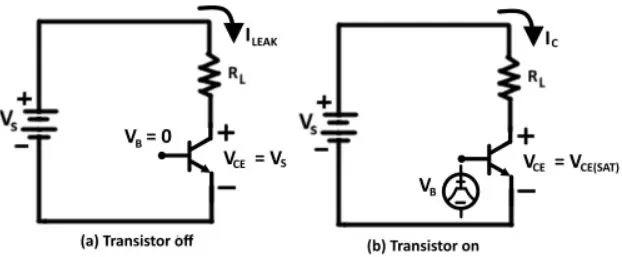
When transistor is in off state:
> When the transistor is in off state then, it carries a leakage current I(leak). The power associated will be
P(off) = Vs * I(leak)
> Since the leakage current is very quite small and does not vary significantly with voltage, its can be neglected and therefore the transistor power loss is essentially zero.
When the transistor is in on state:
> When the transistor is in on state a small voltage drop occurs across it. This voltage is known as saturated voltage Vce(sat)
> The transistor's power dissipation or conduction loss due to saturation voltage is
P(on) = Vce(sat) * Ic
where, Ic = (Vs - Vce(sat))/R
> To control the power for a given application the switch is turned on and off in a periodic manner. Therefore to find the voltage power loss, the duty cycle must be considered.
Pon(avg) = Vce(sat) * Ic * d
Poff(avg) = Vs * I(leak) * (toff/T)
Switching loss
> A real switch have switching loss as it cannot change from on stateto off state instantaniously
> It takes finite times to switch on tsw(on) and off tsw(off). These times not only induces power dissipation but also limits the highest switching frequency possible
The below given image show the switching waveforms of (a) voltage across the switch, (b) current through it and (c) power dissipation.
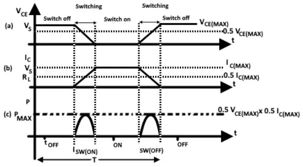
> To find the power dissipated in a transistor during switching interval, we multiply the instantaneous values of Ic and corresponding values of Vce
> The energy dissipated is equal to the area under the power waveform
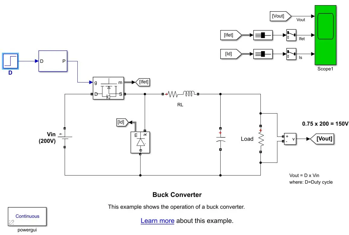
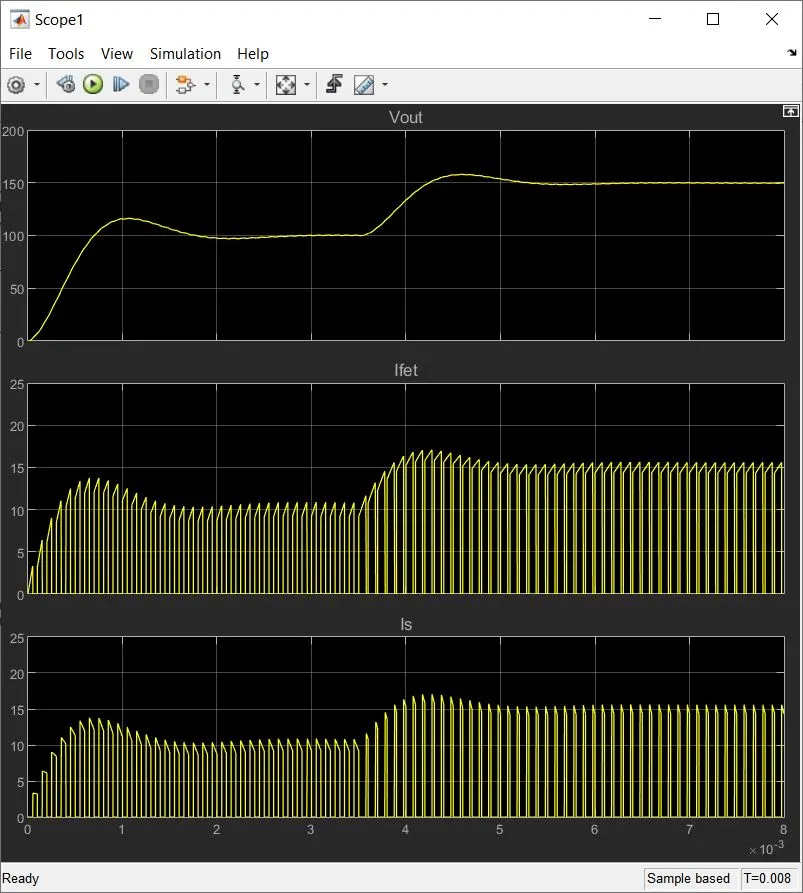
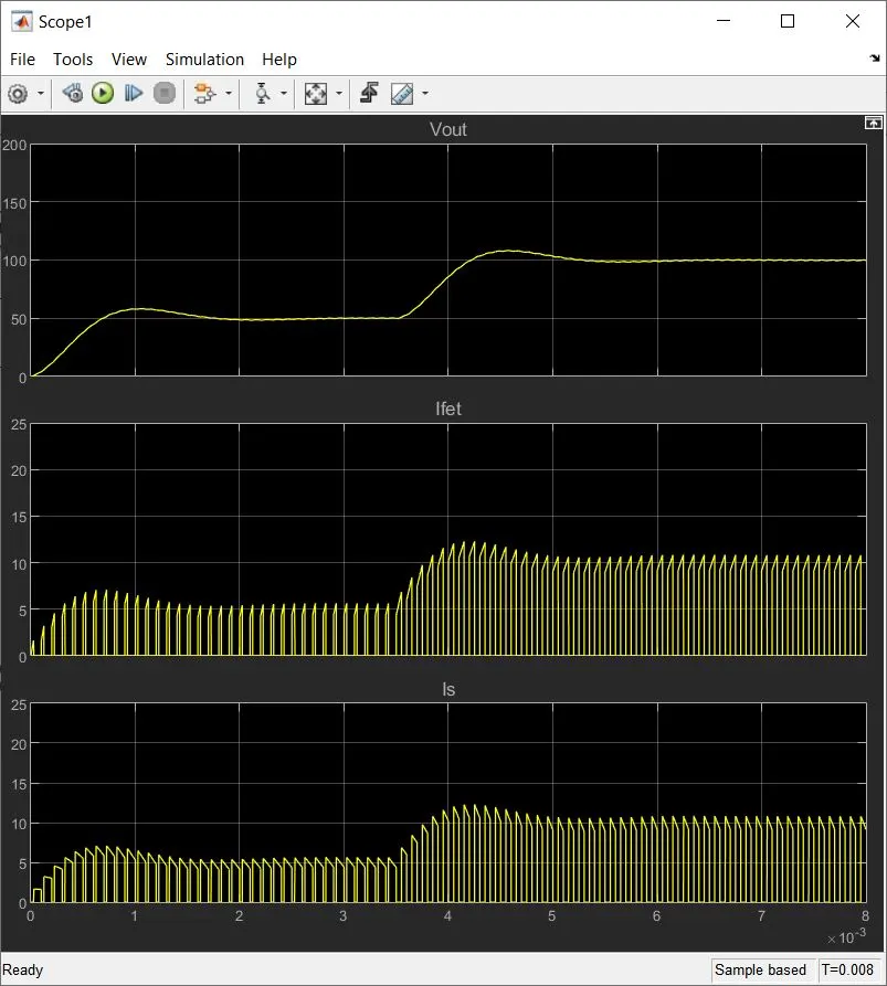
This dc to dc buck converter works in two states, one when switch is closed and second one when switch is opened. When switch is in close state then diode becomes reverse biased then input source provides the energy to inductor as well as output load. Similarly, when switch is in open state then inductor becomes discharged through diode and transfers some of its stored energy to output load. Because the switch is open and close at high frequency therefore higher order of harmonic is generated which are filtered through low pass filter.
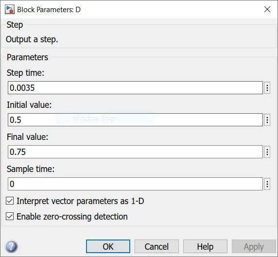
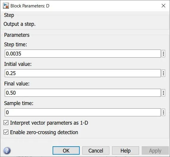
For on or off the switch at high frequency PWM (pulse width modulation) technique is used. The duty cycle of this PWM is calculated by the formula,
D = Vo/Vin
Where, D is duty cycle, Vo is output voltage and Vin is input voltage.
We can see that the output voltage is directly proportional to duty cycle D means which duty ratio is increased then output voltage is also increased as well as when duty cycle is decreased then output voltage is also decreased.
The command (power_BuckConverter) is used to open the buck converter model.The Matlab model is as shown below.
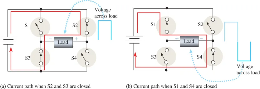
The switch symbols are used to represent switching transistors (IGBTs or MOSFETs) or other types of electronic switching devices. In figure(a) switches S2 and S3 are on for a specified time and S1 and S4 are off. To produce a 60 Hz square wave, each pair of switches is on for half of the period, which is 8.33 ms.
As you can see, the direct current is through the load, which creates a positive output voltage. In Figure (b), opposite switches are on and off. The current is in the opposite direction through the load, and the output voltage is negative. The complete on/off cycle of the switches produces an alternating square wave.
The transistors are switched by a timing control circuit, which is not shown for simplicity. The harmonic distortion of a typical square wave output is in the range of 45%, which can be reduced somewhat by filtering out some of the harmonics.
Motors are the only appliance which supports square wave AC input. Using square wave voltage output creates humming noise in the inverter and the applaince. It also does not guarantee the safety of the appliance but, the price is economical.
Modified sine wave.
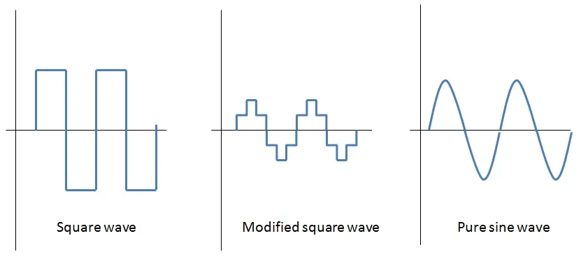
Due to the downsides of the square wave inverter the modified sine wave inverter is used for many applainces with added cost. The modified sine wave compared to a pure sine wave is as show below.
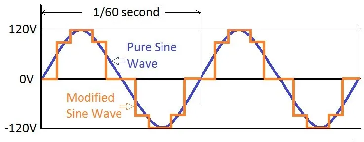
The operation of a basic H-bridge is enhanced to produce the modified sine wave, which is shown in above image. The resulting wave cannot be used for some types of loads. The wave is created from a square wave and adds a short dead time between positive and negatives excursions of the square wave.
Although the resulting output is definitely not a sine wave, the harmonic distortion is reduced to 24% compared to a pure square wave’s 45%. This is still a significant amount of distortion. Filtering can reduce this distortion; however, filtering also significantly reduces the power to the load and thus reduces the efficiency.
A modified sine wave inverter can be used for simple systems that don’t have any delicate electronics or audio equipment that may pick up the choppy wave and produce a hum.
Difference between VFD and Vector control drive.
Variable frequency drive
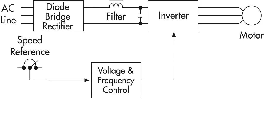
A variable frequency drive controls the speed of an AC motor by varying the frequency supplied to the motor. The drive also regulates the output voltage in proportion to the output frequency to provide a relatively constant ratio of voltage to frequency (V/Hz), as required by the characteristics of the AC motor to produce adequate torque.
> The first step in this process is to convert the AC supply voltage into DC by the use of a rectifier.
> DC power contains voltage ripples which are smoothed using filter capacitors. This section of the VFD is often referred to as the DC link.
> This DC voltage is then converted back into AC. This conversion is typically achieved through the use of power electronic devices such as IGBT power transistors using a technique called Pulse Width Modulation (PWM).
> The output voltage is turned on and off at a high frequency, with the duration of on-time, or width of the pulse, controlled to approximate a sinusoidal waveform.
> The process is controlled by a micro processor
The block diagram of the PWM VFD is given below
Vector control drive
Vector control, also called field-oriented control (FOC), is a variable frequency drive (VFD) control method in which the stator currents of a three phase AC electric motor are identified as two orthogonal components that can be visualized with a vector. One component defines the magnetic flux of the motor, the other the torque.
> The control system of the drive calculates the corresponding current component references from the flux and torque references given by the drive's speed control.
> Proportional integral (PI) controller are used to keep the measured current components at their reference values.
> The pulse width modulation of the variable-frequency drive defines the transistor switching according to the stator voltage references that are the output of the PI current controllers.
> FOC is used to control AC synchronous and induction motors. It was originally developed for high-performance motor applications that are required to operate smoothly over the full speed range, generate full torque at zero speed, and have high dynamic performance including fast acceleration and deceleration.
> With increasing computational power of the microprocessors it will eventually nearly universally displace single-variable scalar volts-per-Hertz (V/f) control.
The field of current block diagram is as shown below
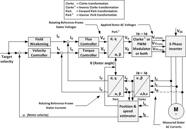
Vector control accordingly generates a three-phase PWM motor voltage output derived from a complex voltage vector to control a complex current vector derived from motor's three-phase stator current input through projections or rotations back and forth between the three-phase speed and time dependent system and these vectors' rotating reference-frame two-coordinate time invariant system.
Such complex stator current space vector can be defined in a (d,q) coordinate system with orthogonal components along d (direct) and q (quadrature) axes such that field flux linkage component of current is aligned along the d axis and torque component of current is aligned along the q axis. The induction motor's (d,q) coordinate system can be superimposed to the motor's instantaneous (a,b,c) three-phase sinusoidal system as shown in accompanying image (phases b & c not shown for clarity).
Projections associated with the (d,q) coordinate system typically involve
> Forward projection from instantaneous currents to (a,b,c) complex stator current space vector representation of the three-phase sinusoidal system.
> Forward three-to-two phase, (a,b,c)-to-(`alpha,beta`) projection using the Clarke transformation. Vector control implementations usually assume ungrounded motor with balanced three-phase currents such that only two motor current phases need to be sensed.
> Also, backward two-to-three phase,(`alpha,beta`)-to-(a,b,c) projection uses space vector PWM modulator or inverse Clarke transformation and one of the other PWM modulators.
> Forward and backward two-to-two phase,(`alpha,beta`)-to-(d,q) and (d,q)-to-(`alpha,beta`) projections using the Park and inverse Park transformation, respectively.
While (d,q) coordinate system rotation can arbitrarily be set to any speed, there are three preferred speeds or reference frames:
> Stationary reference frame where (d,q) coordinate system does not rotate;
> Synchronously rotating reference frame where (d,q) coordinate system rotates at synchronous speed;
> Rotor reference frame where (d,q) coordinate system rotates at rotor speed.
Decoupled torque and field currents can thus be derived from raw stator current inputs for control algorithm development.
Conclusion
> It is concluded that by using variable frequency drive only the frequency is controlled and therefore the torque of the motor is controlled
> By using the vector control method the Flux and Torque are decoupled and can be controlled seperately and the starting torque is higher than the variable frequency drive.
VFD method for induction motor in EV application
If a variable frequency drive is used for an induction motor then the torque vs speed characteristics will be as shown in the below figure.
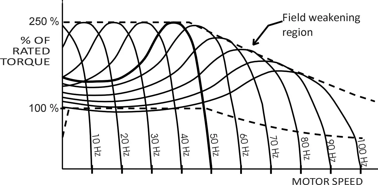
> It is seen that the torque of the motor can be maintained constant for a limited frequency. This is due to the limited voltage supply. Therefore the field weakening region occurs.
> The flux cannot be controlled seperately since, it is coupled with the torque.
> The stator drop compensation is to be considered.
Due to all the above resitrictions the space vector control method is prefered than VFD method for EV application