Duty Cycle
1) Why power electronics circuits are efficient? In practice, which types of losses occur in power electronics circuits?
What is power electronics?
An application of electronics and circuitry that deals with the control and conversion of electrical power from one form to another. They function with the help of power semiconductor devices that operate in a switching mode.
Why are power electronic circuits preferred over linear regulators?
The regulating element in linear regulators is essentially a variable resistor. For instance, if the voltage source has 100V available, but the load requires only 10V, the variable resistor uses up the remaining 90V through the voltage divider concept. Assuming the current in the circuit is 1A, out of the 100W power available, since only 10W is required, 90W is wasted as heat.
In contrast to linear regulators, switching regulators in power electronic circuits exploit the energy storing capacity of LC components. The energy not required by the load is stored in the magnetic field of the inductor L, or in the electric field of the capacitor C. Through pulse width modulation (PWM) and varying duty cycle ratio, the switching regulator ensures that only the required energy is transferred to the load, while the rest is stored.
Types of losses in power electronics:
- Switching losses: Referring to the figure below, when the switch is off, there is a potential difference (voltage) across the two ends of the switch while the current flowing is zero. As soon as the switch is flipped on, there is no potential difference while the current is in full flow. So, when the switch is on or off, because one of voltage and current will be negligible (if not zero), the power dissipated as heat is also zero (since P = VI). It is the transitioning phase when the switch is being turned on or off when both V and I are not zero. This is what causes the power dissipation. The more the switching frequency, the more power lost in the form of heat.
- Conduction losses: when the device is in full conduction, these losses include the typical losses due to the the RLC components. An addition to this would be due to the output diodes. The voltage drop across diodes is much higher than across RLC components.
2) Using a suitable MATLAB model, show how duty cycle control signal can be generated for a simple power converter circuit?
Common power converter circuits include, but are not limited to:
- DC to DC (chopper)
- Buck converter (step down voltage)
- Boost converter (step up voltage) - this question will be explored with reference to a boost converter
- AC to DC (rectifier)
- AC to AC (voltage regulator)
- DC to AC (inverter)
Importance of boost converters
Motors used in HEVs/EVs require high voltages (in the range of 500V) which cannot be supplied by a battery alone. Stacking up multiple batteries wouldn't be the best solution because of the weight and extra space the battery adds and the difficulties associated with battery and thermal management for optimized battery performance. This is where boost converters come in, as fewer batteries could be used but output DC voltage can still be boosted.
How do boost converters work?
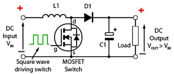
In order to understand the entire circuit, the roles of inductor and capacitor are crucial:
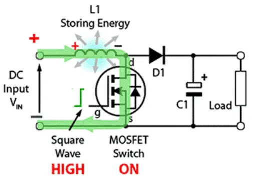
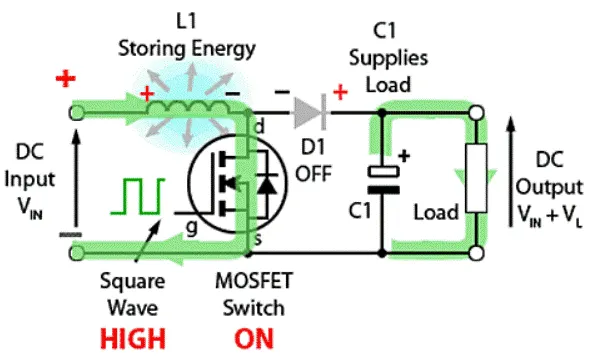
- Referring to the figure 1 above, when the FET switch is ON during the positive half cycle of the DC wave, current flows through the inductor. An inductor is a coil of wire through which current flows, hence inducing a magnetic field that stores energy `V_L`.
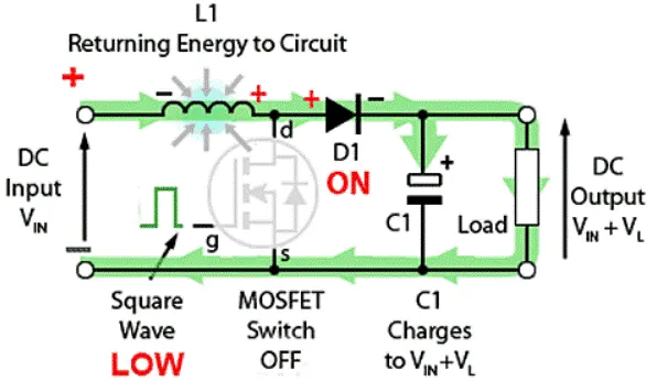
- During the negative half cycle when the FET switch is OFF, there is nothing to hold the induced magnetic field in place, since no new current is flowing through the inductor anymore. The induced magnetic field starts to diminish, and starts to release the stored energy `V_L` (change in field flux in a coil of wire induces current flow). Now current flows to the capacitor (an element that stores energy) and the load, charging the capacitor with `V_(IN) + V_L`. The output voltage across the parallelly connected load is also measured as `V_(IN) + V_L`.
- Once the second period starts and the FET switch is ON again, the capacitor releases its energy to increase the potential difference across the load. Due to the diode, the capacitor cannot discharge its energy towards the inductor and all of it flows towards the load.
- This process keeps on repeating as the FET switch is turned on/off multiple times in a single second, and this is how `V_(IN)` gets boosted to `V_(IN) +V_L` for every cycle, until voltage limit is reached for the load.
Duty cycle variation to observe change in output voltage:
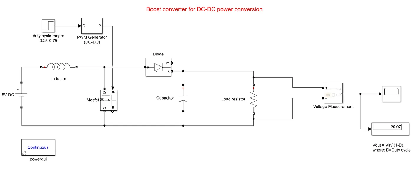
- Above is a simple boost converter model constructed to show the effects of duty cycle ratio
- The duty cycle range has been given from 25% to 75%
- Theoretically, with boost converters, `V_(out)` can be calculated by `V_(out)=V_(IN)/(1-d)`
- So for 25% duty cycle, `V_(out)=5/(1-0.25)=6.67V`, and for 75% duty cycle, `V_(out)=5/(1-0.75)=20V`, which is evident with the 20.07V value
Output:
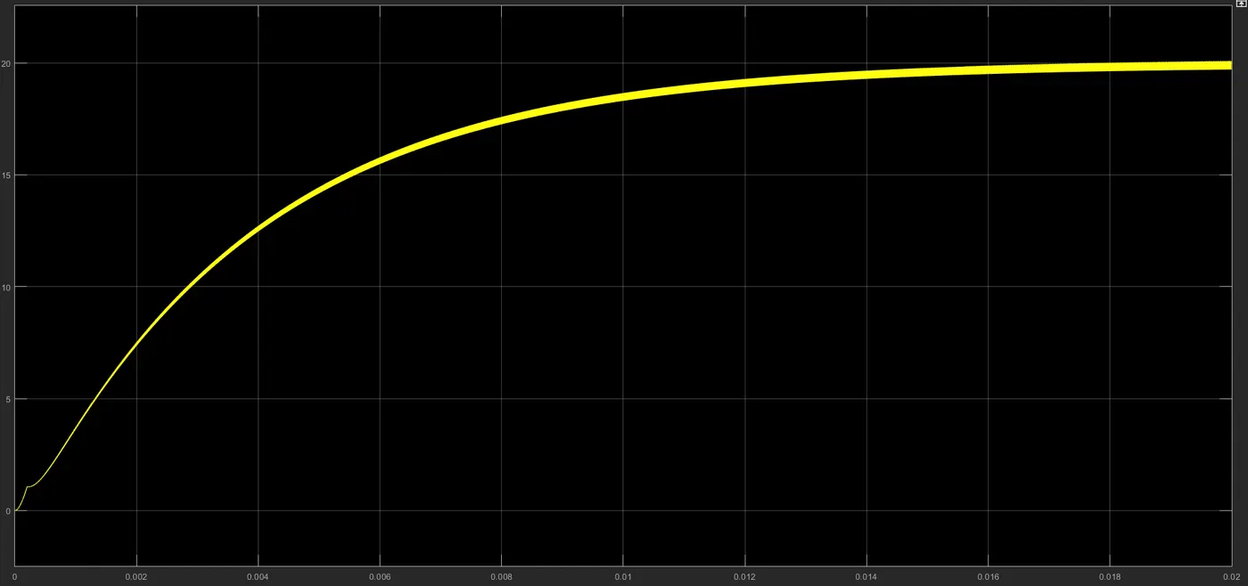
- As is evident, as the duty cycle increases, so does the output voltage
3) Explain the difference between VFD and Vector control drive. Can we use VFD method for induction motor in EV application?
| Variable frequency drive (VFD) | Vector control drive |
|
|