Week 9 - PCB Thermal Simulation
PCB Thermal Simulation
Aim
To conduct the thermal simulation on the PCB model in ANSYS Icepak by importing the PCB layout, library files, and traces. Conduct thermal analysis for the following three scenarios:
Solve the model exclusively for conduction, excluding the components.
Solve the model for forced convection, considering the presence of actual components.
Solve the model for forced convection and trace heating simultaneously.
Objective:
The primary goal of this challenge is to acquire proficiency in PCB modeling concepts and practices, with a focus on the following key aspects:
Learn the process of importing the trace layout of a typical PCB and executing thermal analysis for two specific scenarios based on the trace layout information.
Explore the utilization of the "Model layers separately" option to enhance accuracy in modeling.
Gain expertise in modeling resistive heating or Joule heating associated with the imported traces on the PCB.
Comprehend the implementation of varying orthotropic conductivity on the board through the utilization of a profile mesh size.
Develop a comprehensive conductivity map of the PCB to facilitate a detailed understanding of thermal characteristics.
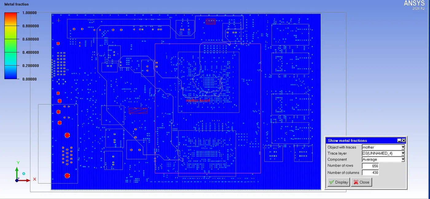
PCB-traces
The images attached below show the PCB-traces using different display options
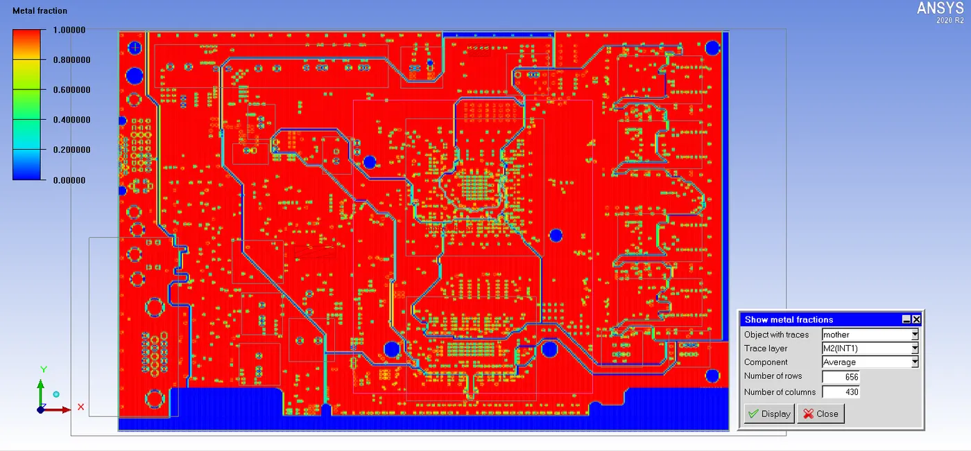
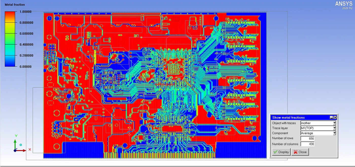
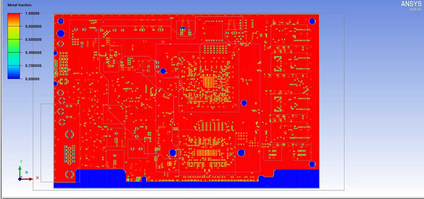
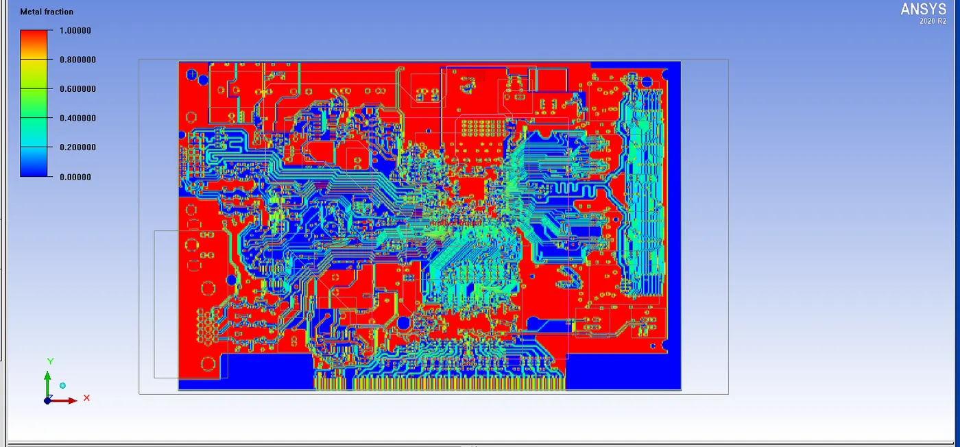
Thermal conductivity contours
The images attached below show the kX thermal conductivity contours are plotted over the Z-plane passing through the center of the PCB.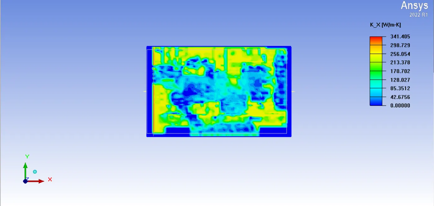
Forced convection model
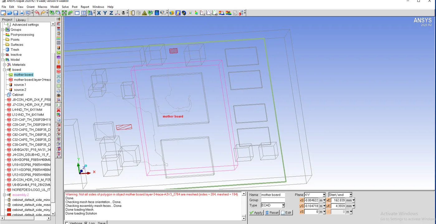
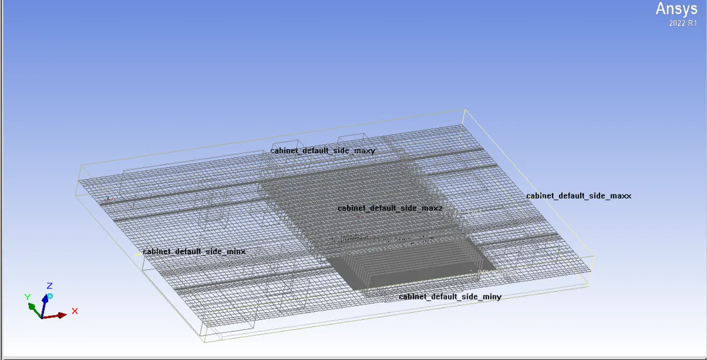
I. Geometry
The image attached below shows the geometry of the model
.
Meshing
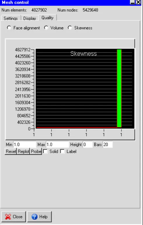
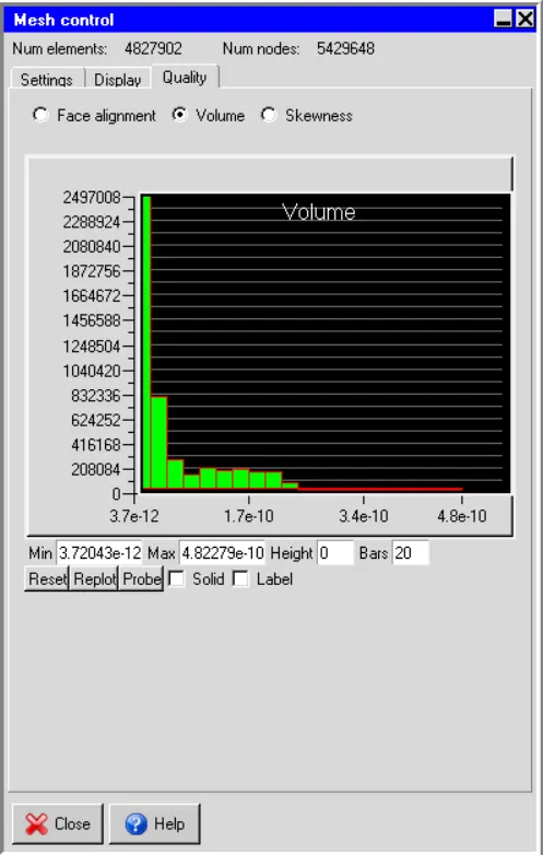
The computational domain is discretized using the Hex-dominant grid generated by the Mesher-HD of 137268 mesh elements and 146080 nodes
.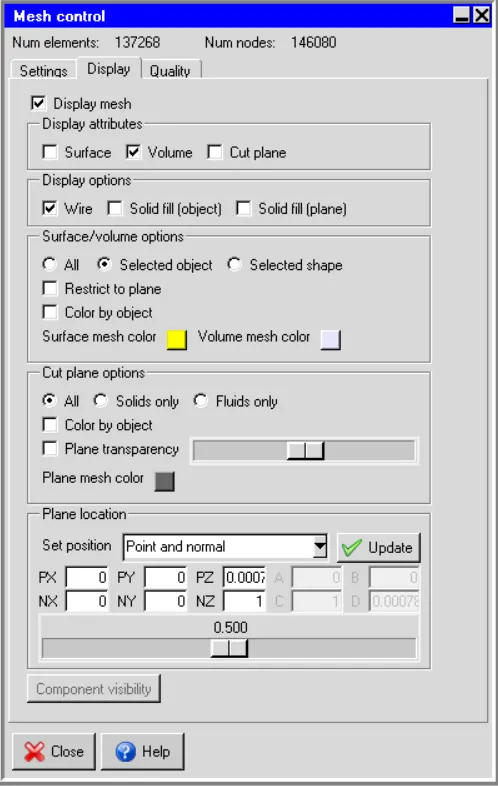
The mesh showed good quality of mesh
Results
This section presents an examination of the simulation outcomes.
Residuals
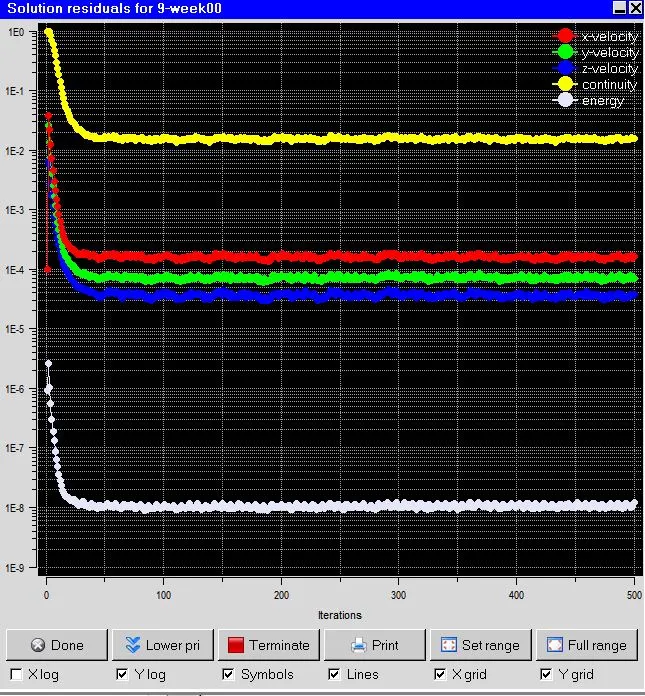
Graphs depicting the residuals for the following equations are plotted against the 500 number of iterations
:
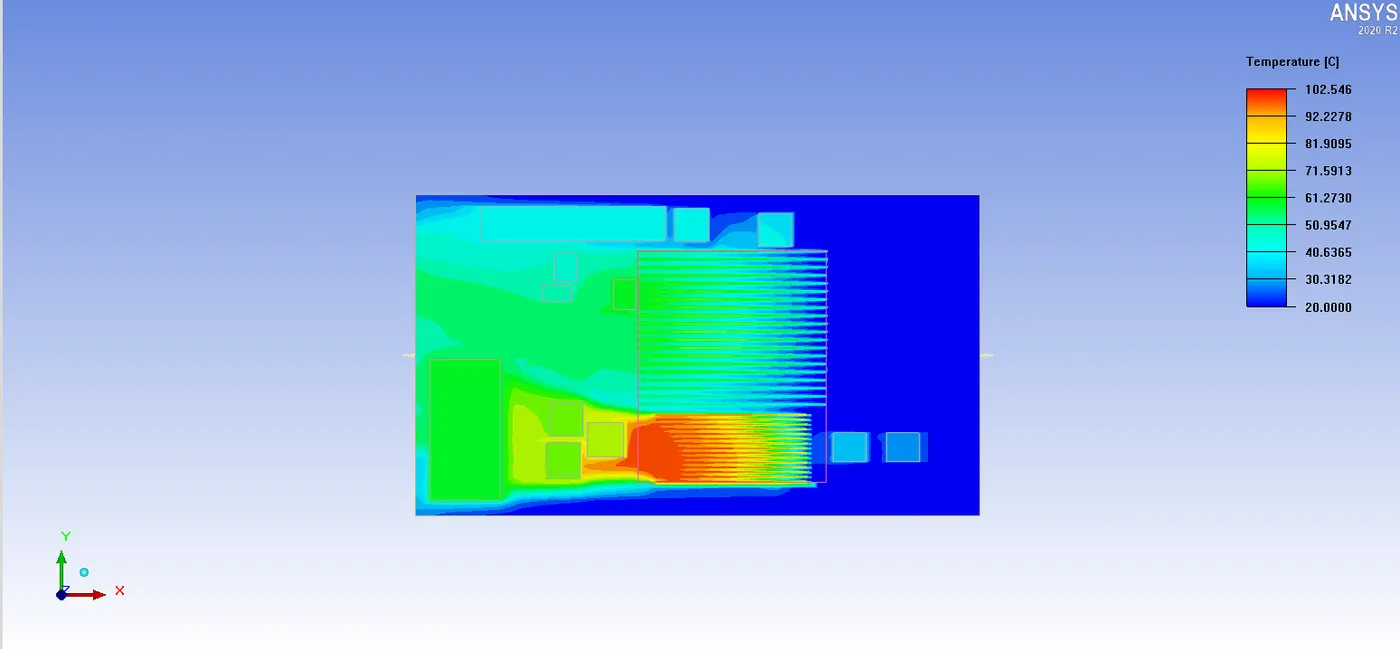
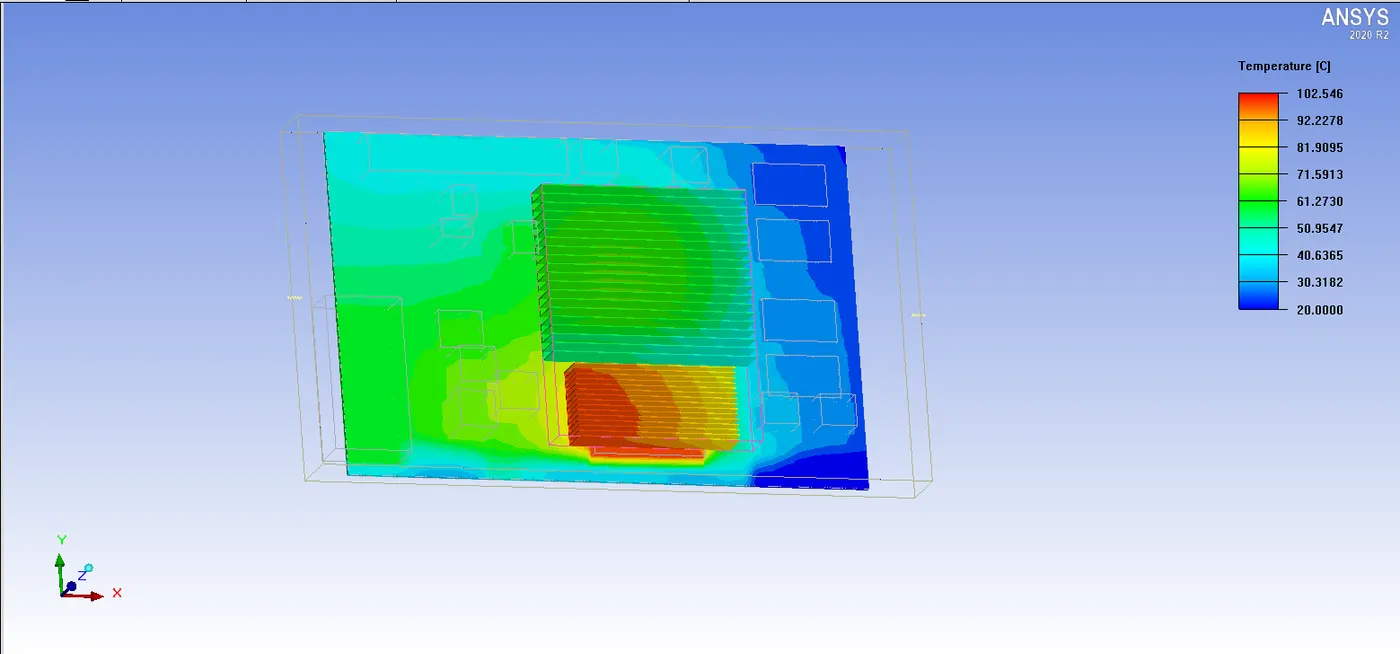
Temperature
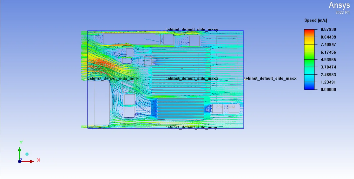
The heatsink was provided with power inputs of 65 W and 75 W for the respective packages below it and the X min was given of 2 m/s
Velocity
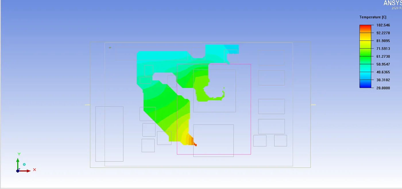
Simulating Forced Convection Cooling of the PCB model with the trace Heating
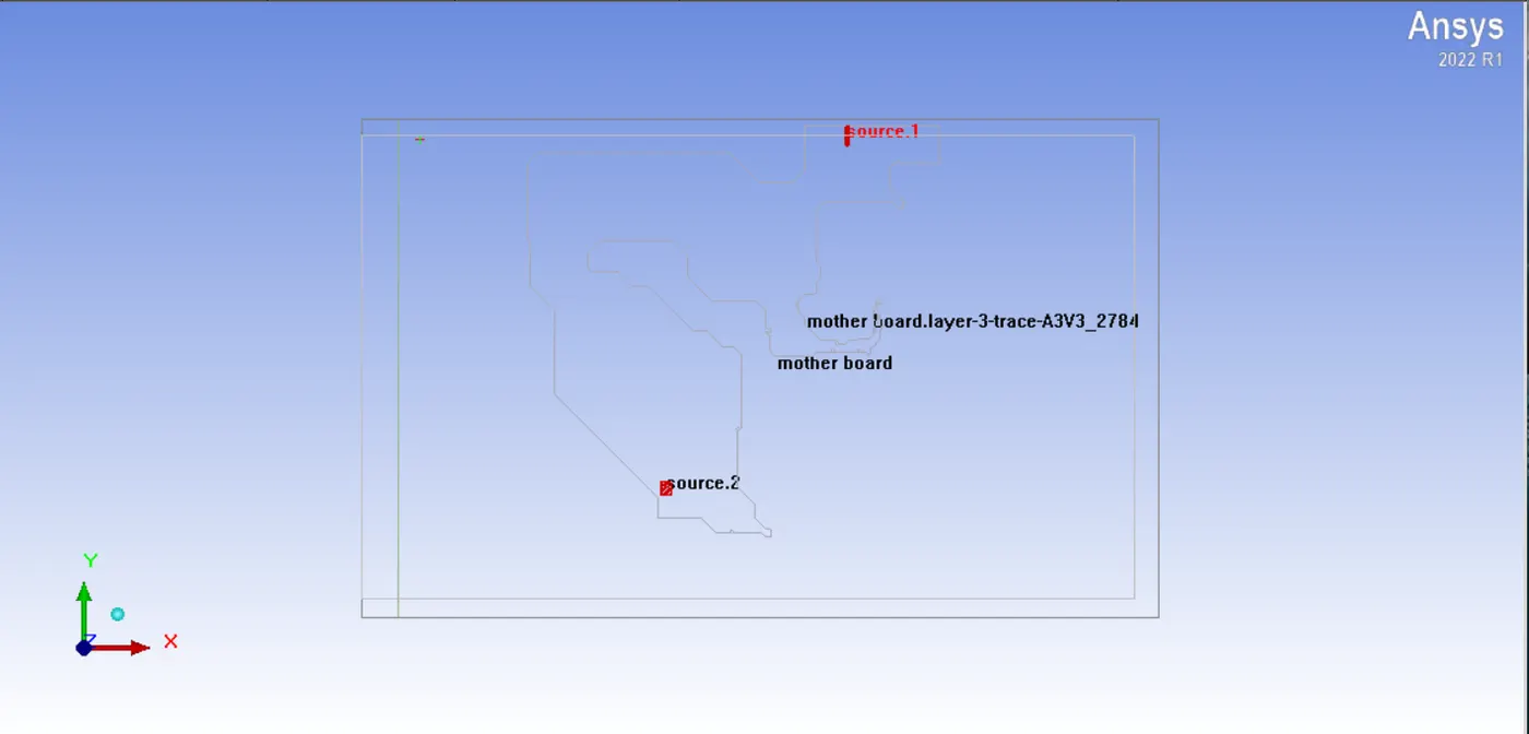
2 source are added mother board layer 3 trace A3V3-2784 with 20A and 0 V for Joule heating
Result
Conclusion
1. The given board file and ECAD file were imported to ANSYS Icepak.
2. All the components on the PCB were deactivated and the resulting model was solved only for conduction.
3. Key components on the PCB are activated and the resulting model was solved for forced convection.
4. In order to model trace heating, a solid trace was created using the identified trace and two voltage/current type sources were created using appropriate settings. The resulting model was solved for forced convection and trace heating.