Week 9 - PCB Thermal Simulation
AIM : To Simulate a Thermal analysis of PCB model by importing the given PCB layout, library files and traces in Ansys ICEPAK.
OBJECTIVES :
- Import the given PCB model, with library and Traces.
- Performing the Thermal conductivity analysis of Just the PCB board
- Simulating Forced Convection Cooling of the Whole PCB model with Components.
- Create optimal meshing for the model.
- Setup the model for the Analysis.
- Run the simulation and Post Process the results.
- Simulating Forced Convection Cooling of the PCB model with the trace Heating.
INTRODUCTION :
A printed circuit board (PCB) mechanically supports and electrically connects electronic components using conductive tracks, pads and other features etched from one or more sheet layers of copper laminated onto and/or between sheet layers of a non conductive substrate. Components are generally soldered onto the PCB to both electrically connect and mechanically fasten them to it.
A basic PCB consists of a flat sheet of insulating material and a layer of copper foil, laminated to the substrate.
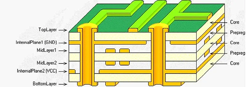
Main Components of a PCB ( in Mechanical/Thermal Aspect )-
- Board - Generaly FR4 is used for Insulated support, layered with Copper foil layer on which the circuit is made.
- Traces - Trace heating is important part to be considered while thermal modeling, However it can be ignored for many of the electronics which do not operates on high currents, but are imprtant to considered in Power Electronics.
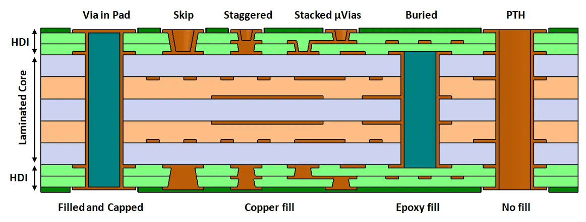
- Vias - are the electrical connection between copper layers in a printed circuit board. However, the vias also passively used to pass heat from top to bottom or vice versa. Vias contribute in increasing the lumped thermal conductivity of the PCB.
ANALYSIS :
1) Thermal conductivity Analysis of the PCB
1.1 Geometry
Unpacking the given trace.tzr file of the PCB and the all the components are set to inactive.
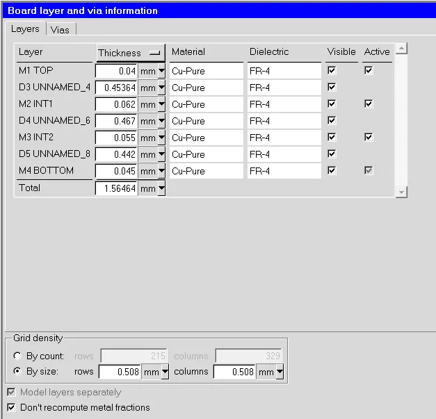
Importing the ECAD file A1.anf and edit the thickness layer for the model and the grid density is set at 0.508mm * 0.508mm.
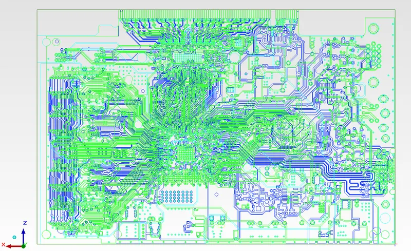
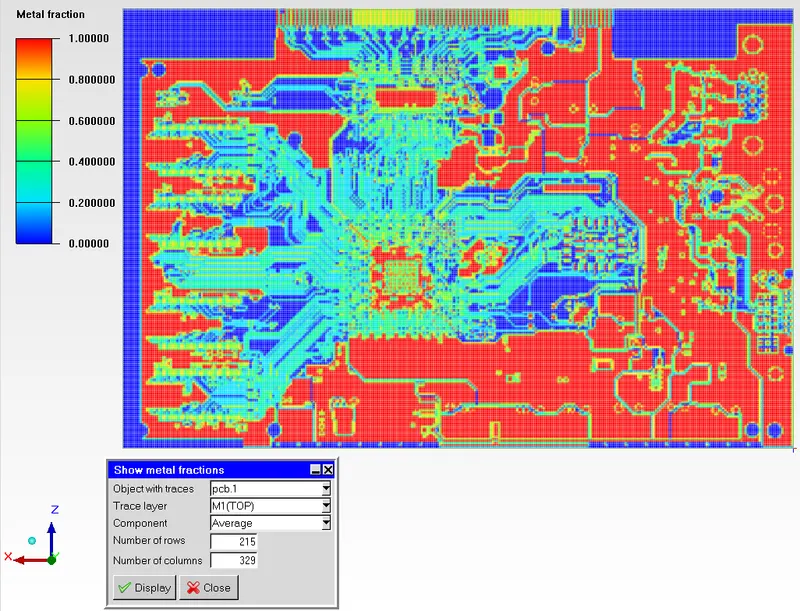
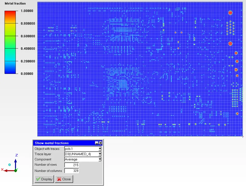
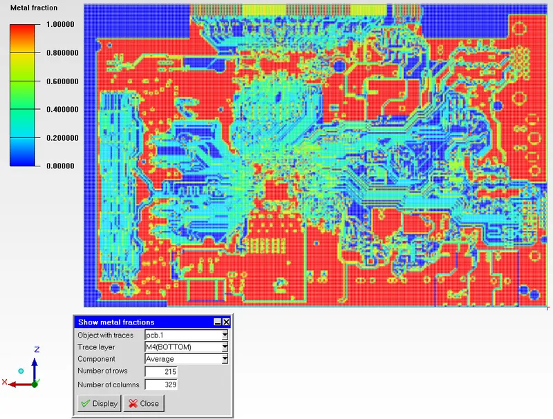
After loading the ECAD of the PCB, we can see the traces of PCB and compute and view the Metal Fraction distribution across the layers.
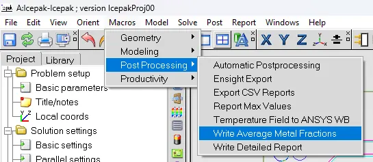
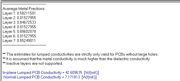
As from above we can see the metal fraction percentage at each layer and also can see the lumped thermal conductivity of the whole PCB.
Layer 1
Layer 2
Layer 3
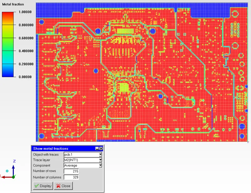
Layer 4
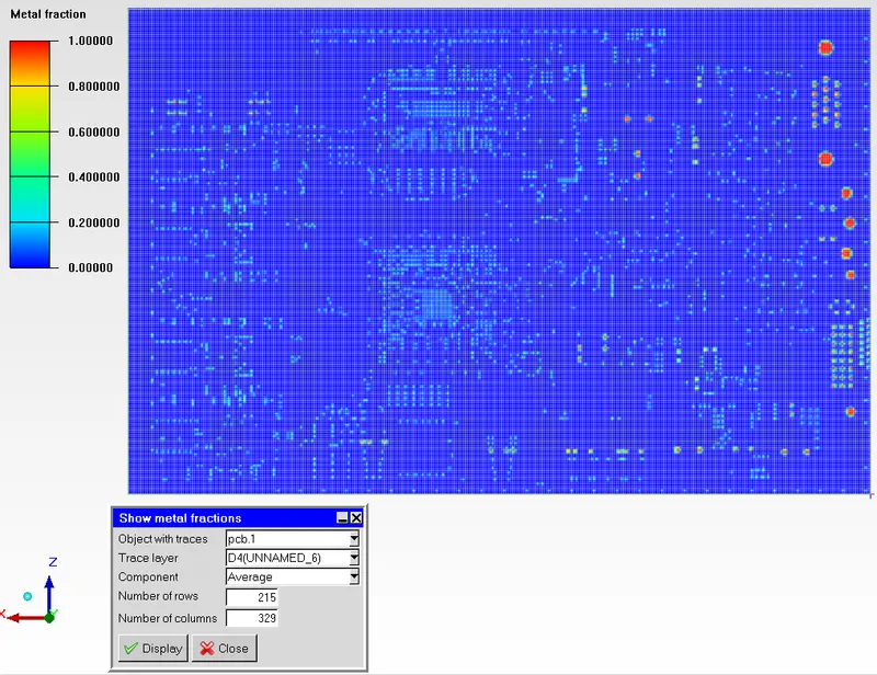
Layer 5
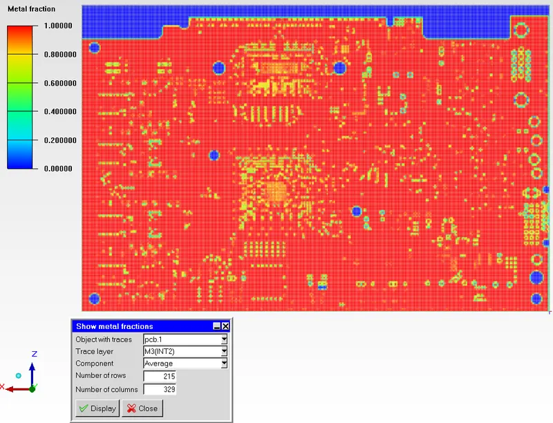
Layer 6
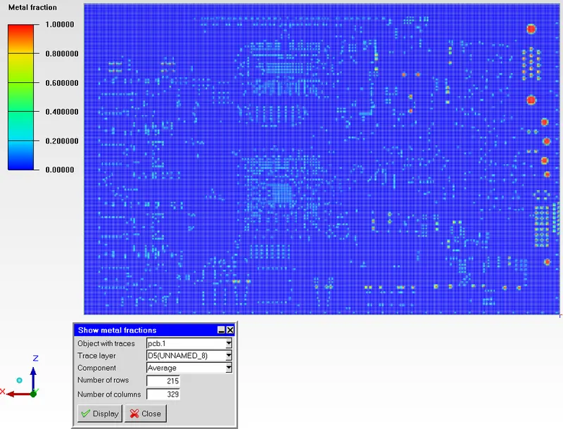
Layer 7
Now Proceeding towards Analysis.
1.2 Meshing
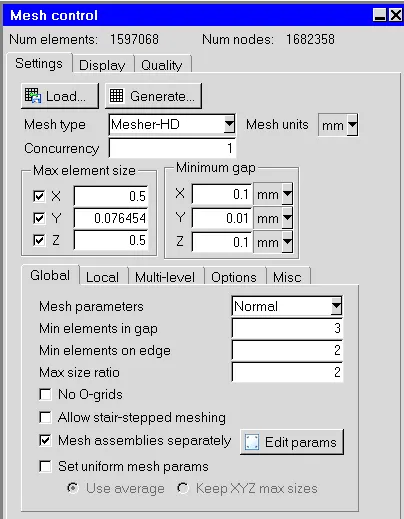
Following is setting used for global mesh and the assembly mesh settings -
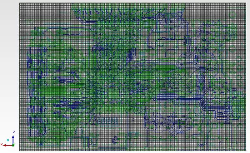
Following is the surface mesh of the PCB -
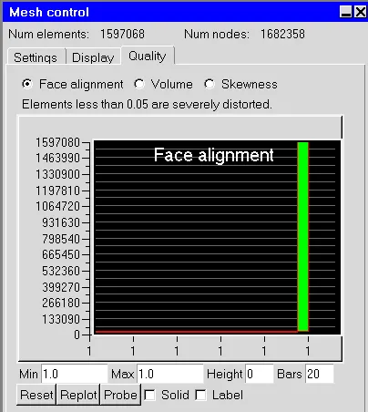
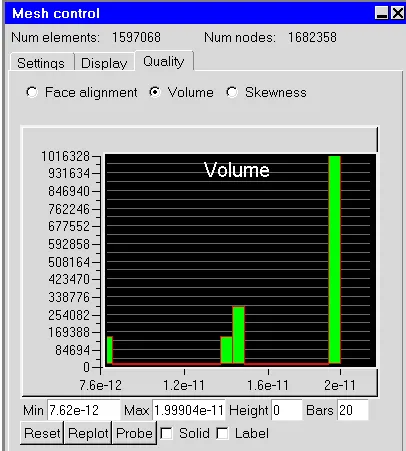
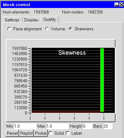
The mesh quality looks fine we can proceed towards assing properties and solver setup.
1.3 Properties and Boundary Conditions
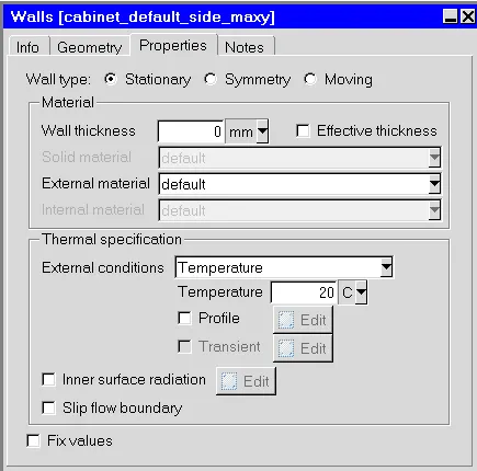
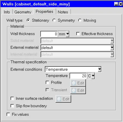
1.4 Solver Settings
Since we are just checking for the Thermal conductivity of the board, we will only simulate for the thermal conduction.
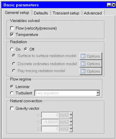
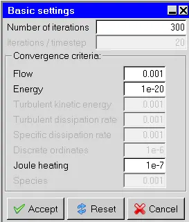
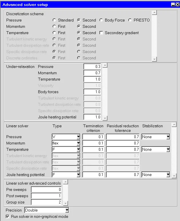
The solver setting majorily have kept default. and the discretization schemes are kept 2nd order in-order to more accuracy after running first cut simulation 1st order scheme
1.5 Results
Residuals and Monitor Points -
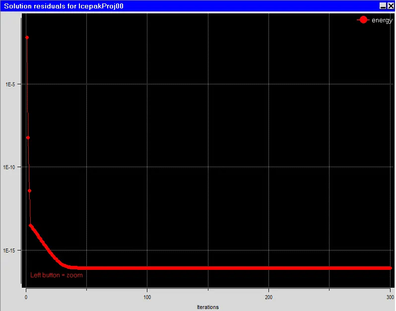
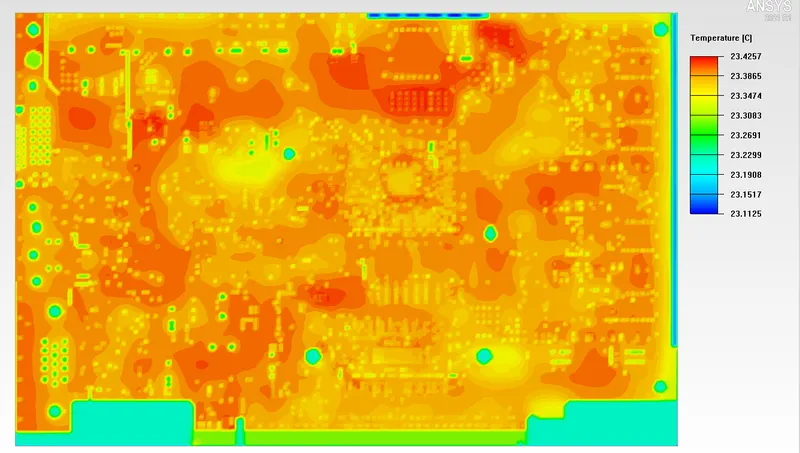
Temperature Contours -
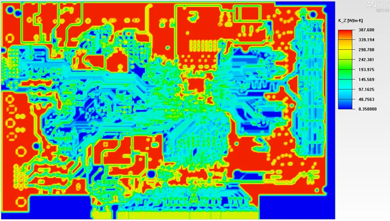
Thermal Conductivity Contour along (In-plane Thermal Conductivity) Z Direction at Different layers of the PCB -
Layer 1
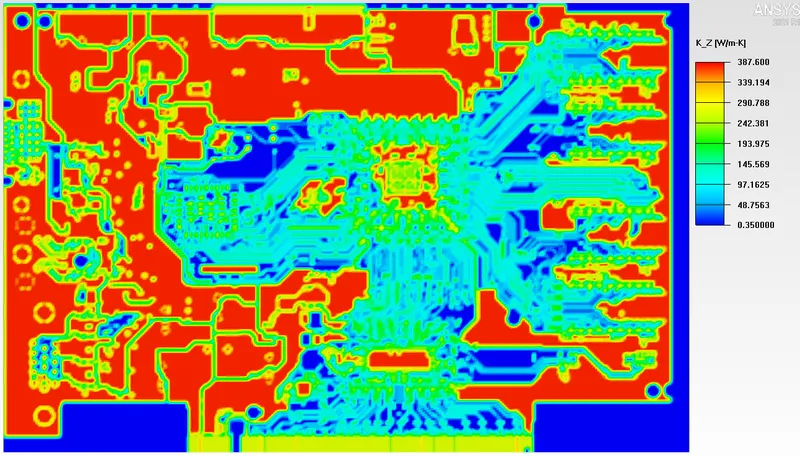
Layer 3
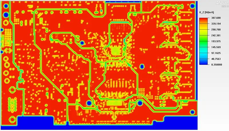
Layer 5
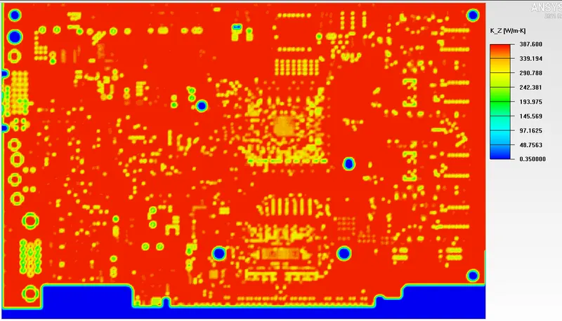
Layer 7
2) Simulating Forced Convection Cooling of the Whole PCB model with Components
2.1 Geometry
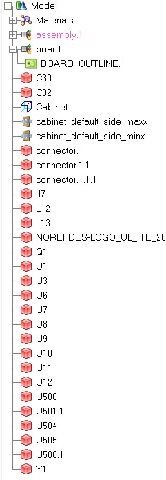
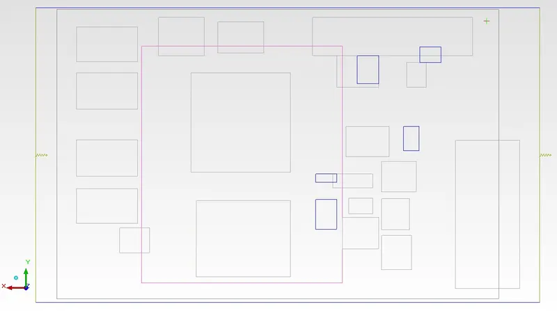
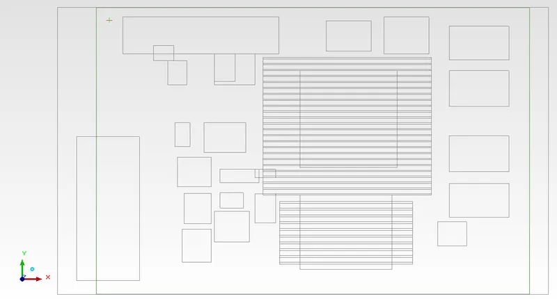
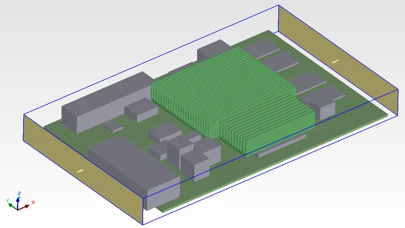
The System setup of as follows, now all the pcb mounted components are active and will also particpate in the thermal cooling of the PCB with forced convection cooling -
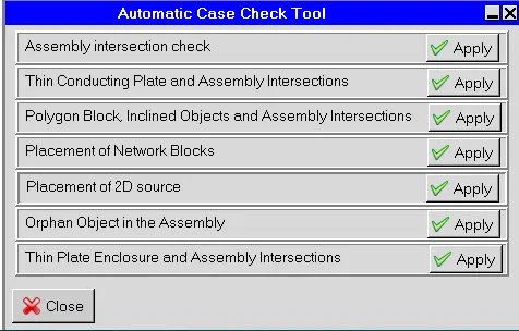
Case check tool in Macros options-

2.2 Meshing
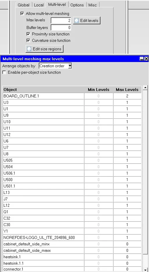
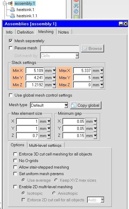
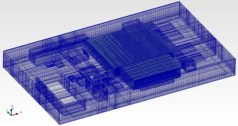
We have created a non-conformal mesh assembly accross the component assembly. To have fine mesh near to the components and coarser mesh across the enclosure and its ambient.
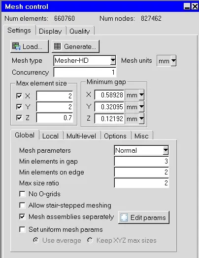
Following is setting used for global mesh and the assembly mesh settings -
Following is the surface mesh of the Case Setup -
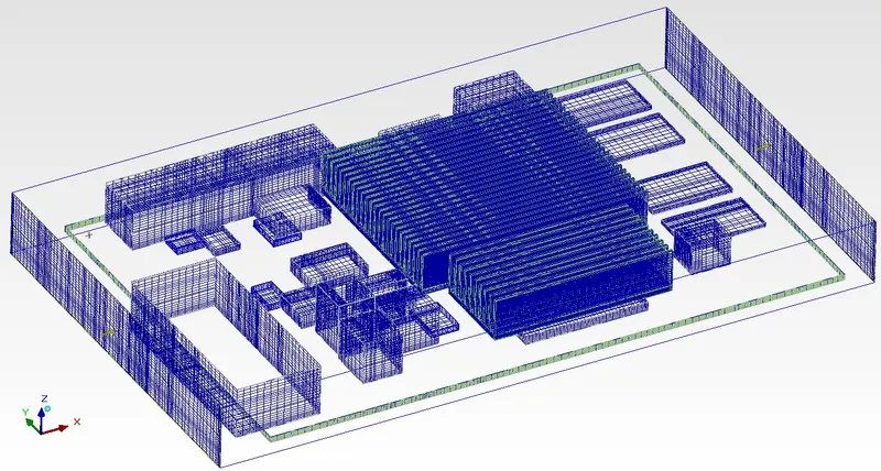
Following is the visualising the mesh inside the cabinet-
- Cut plane of XY plane at an offset from top of the cabinet in Z-direction from origin (Top Plane)
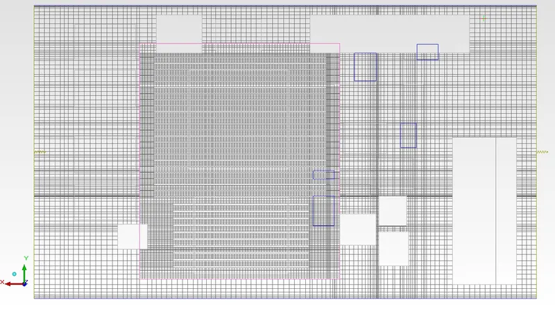
- Cut plane of XY plane at an offset from top of the cabinet in Z-direction from origin (Top Plane)
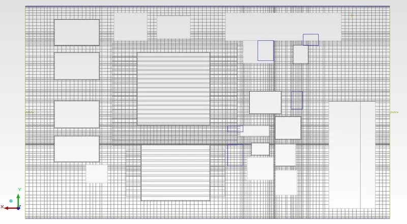
- Cut plane of XZ plane at 50% of the cabinet in Y-direction from origin (Right Plane)

- Cut plane of YZ plane at 50% of the cabinet in X-direction from origin (Front Plane)

Mesh Quality Parameters -
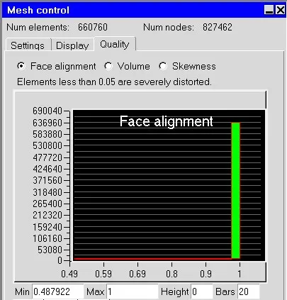
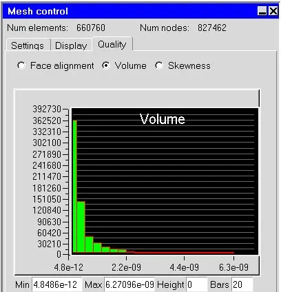
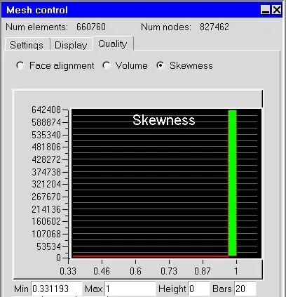
We can the mesh quality is very satisfied. 90% of the mesh cell are lying on good quality range.
2.3 Solver Settings
Now we are solving for the forced Convection cooling, therefore turning on the Flow solver, and the respective settings are as follows -
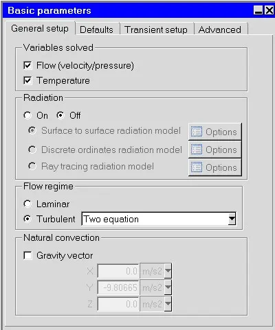
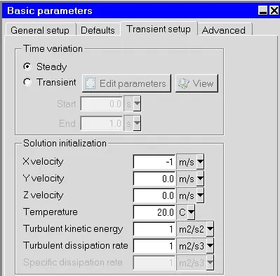
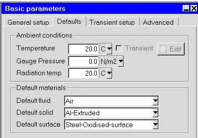
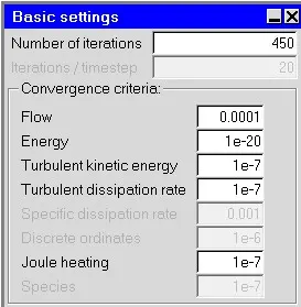
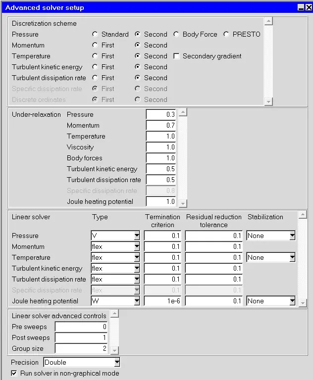
Gravity and Radiation options are turned off since the majority of the fluid flow and heat transfer due to Forced convection.
Inorder to capture the turbulence flow conditions we have chosen two equation model option i.e. K-epsilon turbulance model. Since, vortices / turbluence plays major roll in the heat transfer and therefore cooling.
2.4 Results
Residuals and Monitor Points -
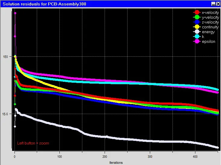
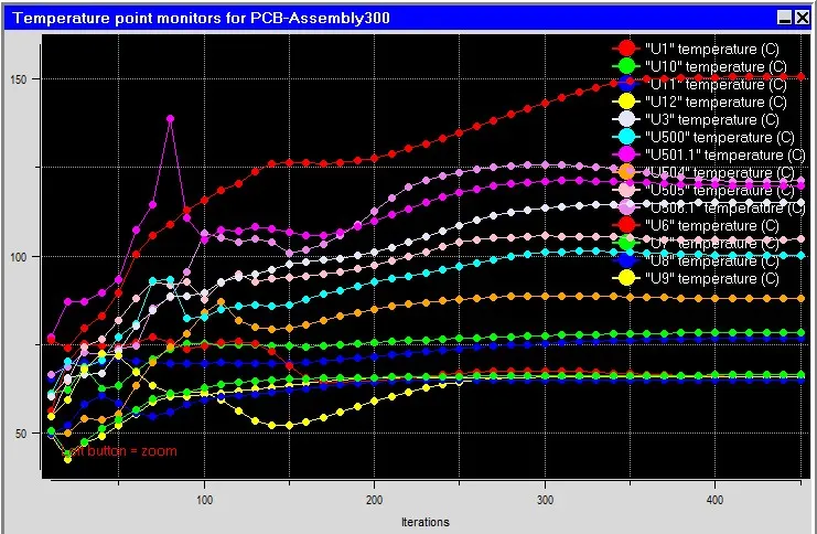
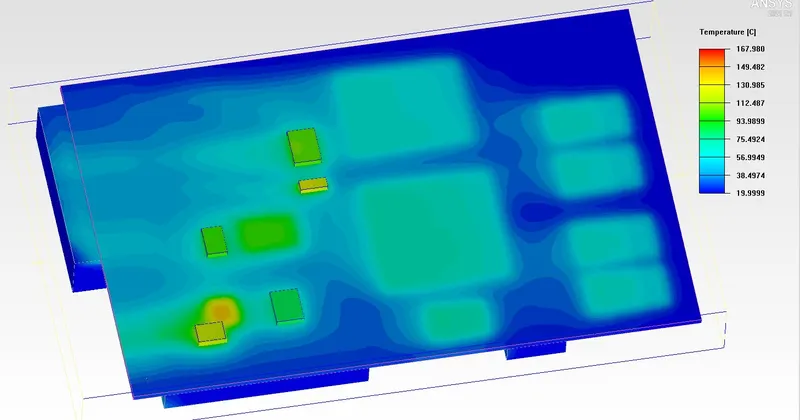
Temperature Contours -
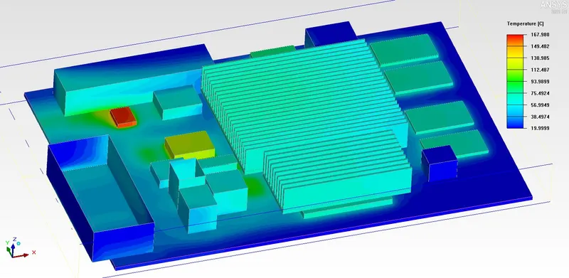
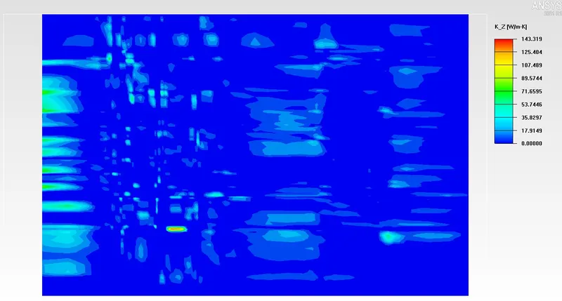
Thermal Conductivity Contour along (In-plane Thermal Conductivity) Z Direction at a mid layer of the PCB -
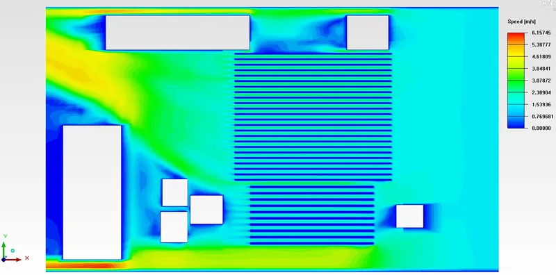
Contour Visulization of Velocity of the fluid -
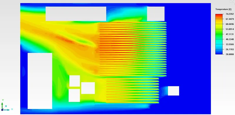
Temperatures Visulization of the fluid volume passing through and taking heat -
3) Simulating Forced Convection Cooling of the PCB model with the trace Heating
3.1 Geometry
In This Version of the analysis, the geometry of the system is same as the previous, just there's an addition of trace study as shown below -
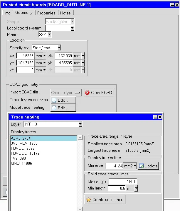
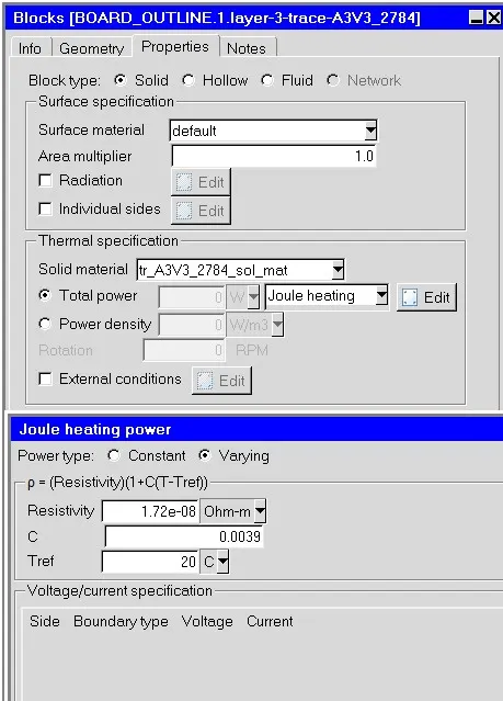
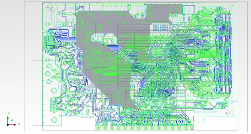
Following we can see the respective solid trace of the PCB layer -
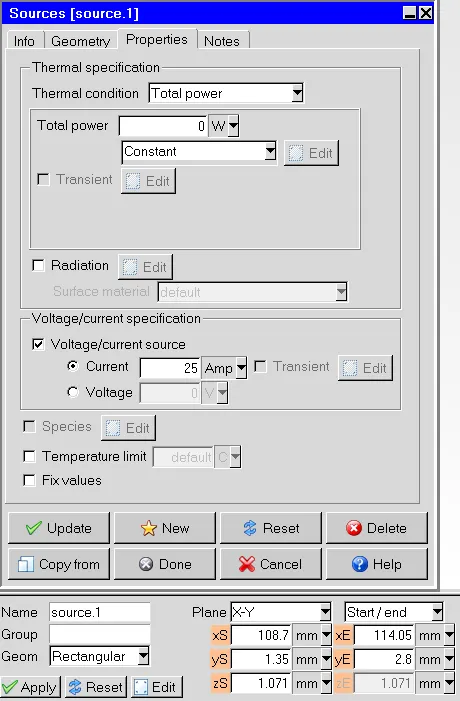
3.2 Assigning the Properties and boundary conditions -
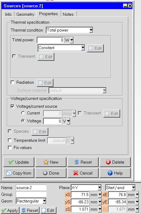
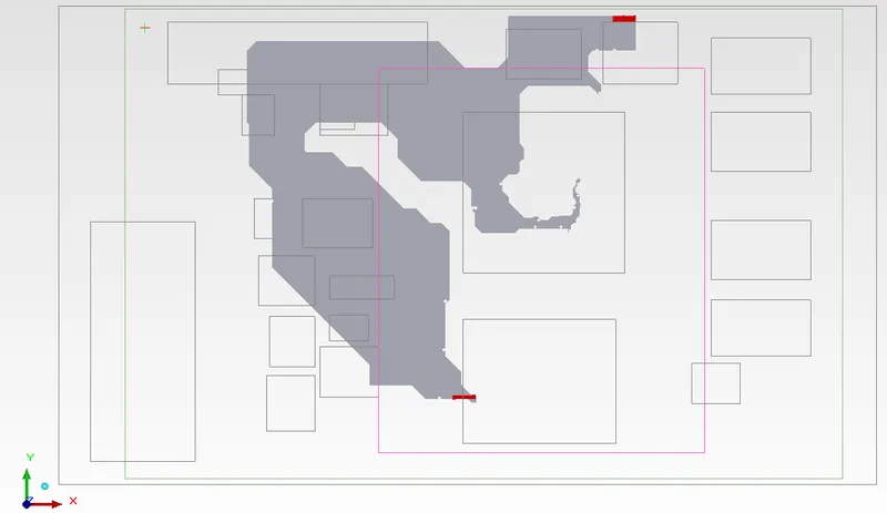
3.3 Meshing
The Meshing settings are similiar as the previous analysis, but they have been made more refined in this analysis inoreder to increase accuracy.
Following are mesh settings and the values -
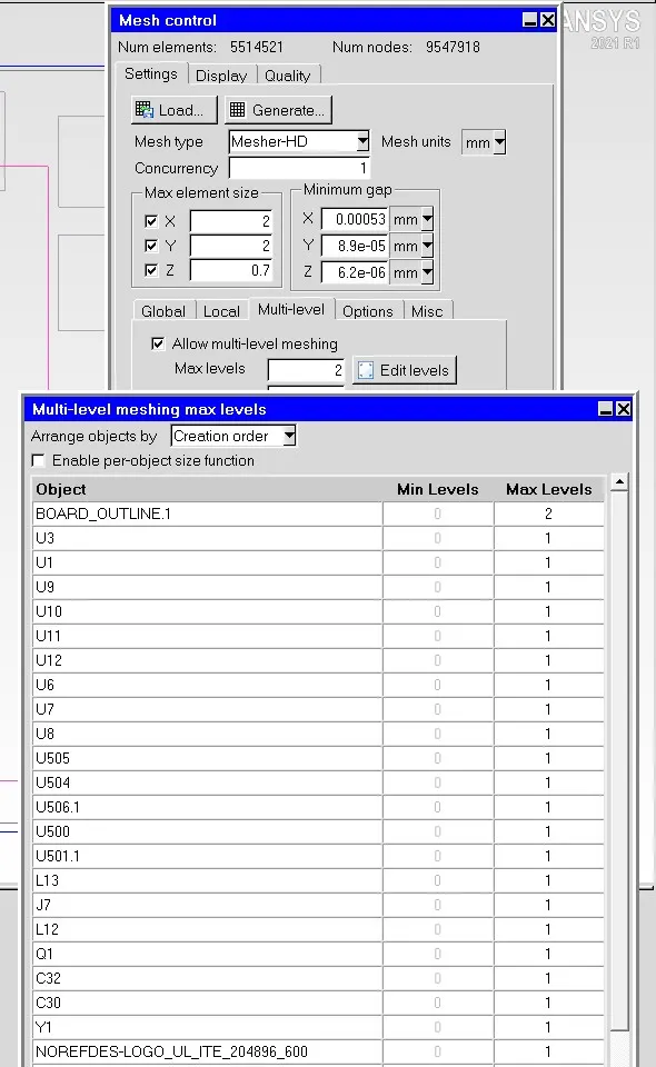
Following is the surface mesh of the Case Setup -
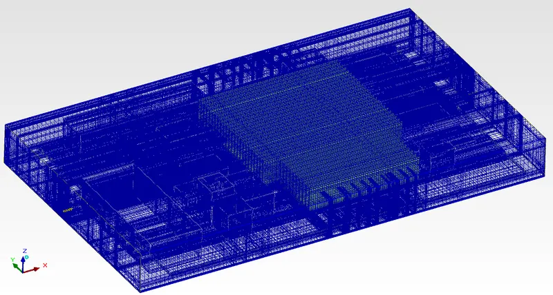
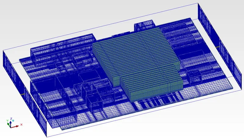
- Cut plane of XY plane at 50% of the cabinet in Z-direction from origin (Top Plane)
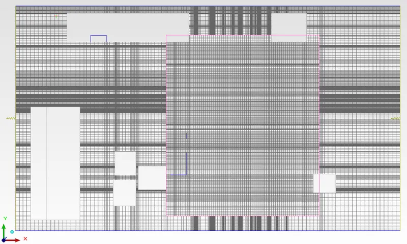
- Cut plane of XZ plane at 50% of the cabinet in Y-direction from origin (Right Plane)

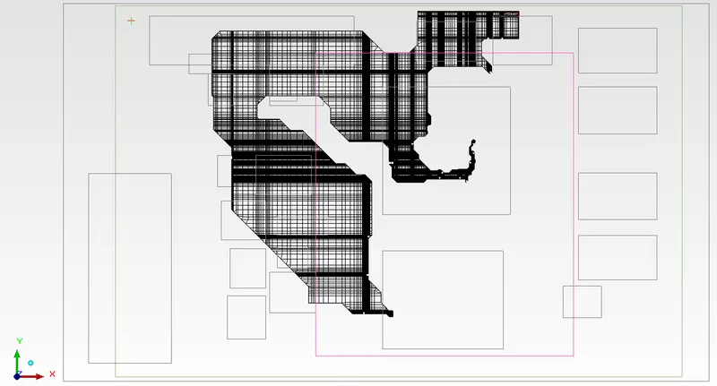
- Mesh across the solid trace of the PCB.
Mesh Quality Parameters -
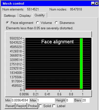
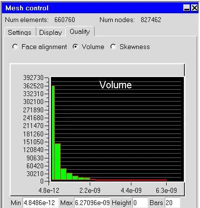
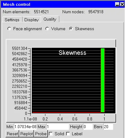
We can the mesh quality is very satisfied. 90% of the mesh cell are lying on good quality range.
2.4 Solver Settings
Following the Solver Settings, which are similar to the previous analysis -
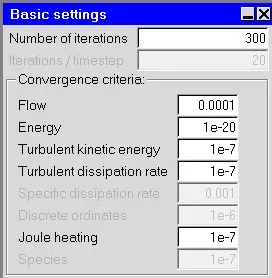
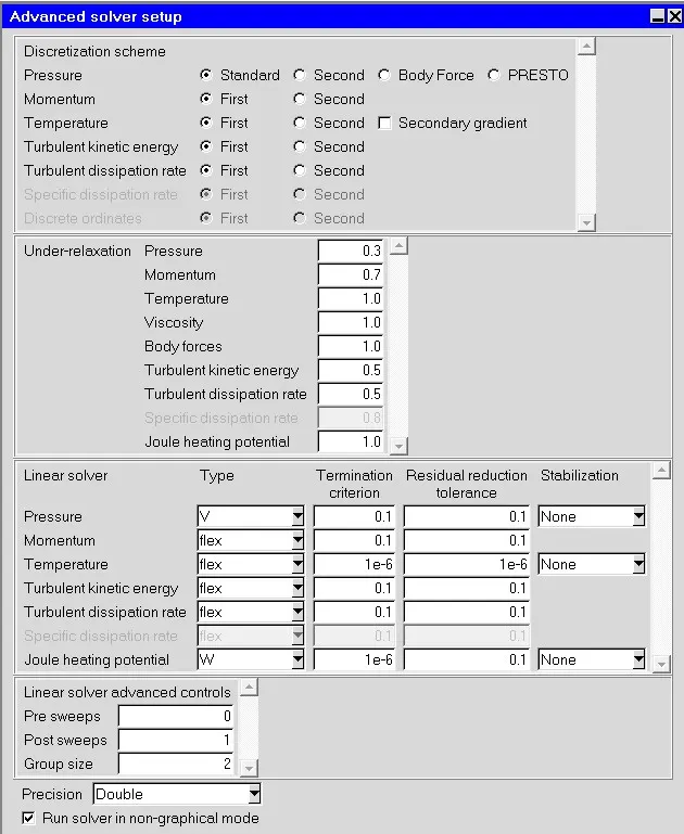
Assigning Monitor Points -
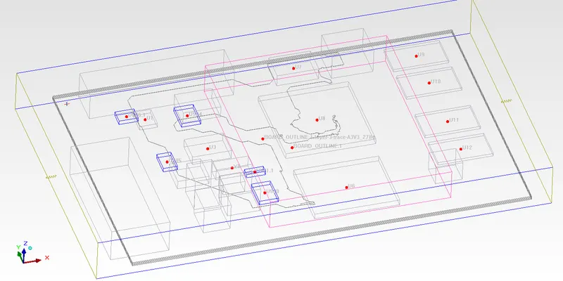
3.5 Results
Residuals and Monitor Points -
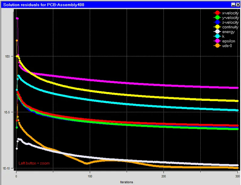
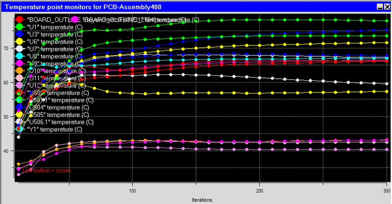
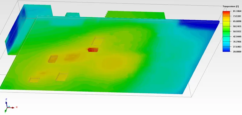
Temperature Contours -
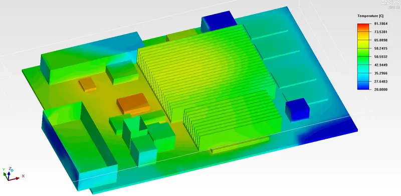
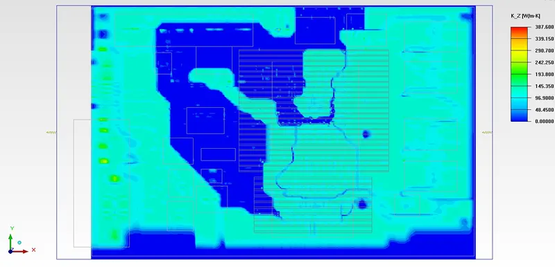
Thermal Conductivity Contour along (In-plane Thermal Conductivity) Z Direction at a mid layer of the PCB -
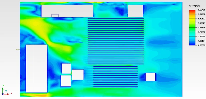
Contour Visulization of Velocity of the fluid -
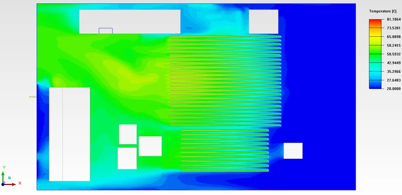
- Temperatures Visulization of the fluid volume passing through and taking heat -
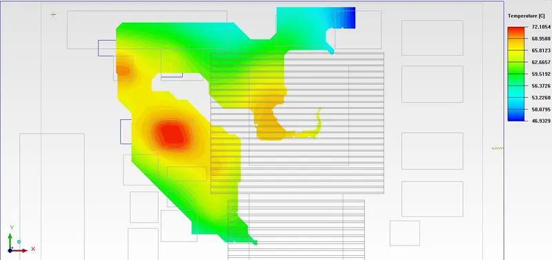
- Temperature Contour at the Selected Solid Trace of the PCB
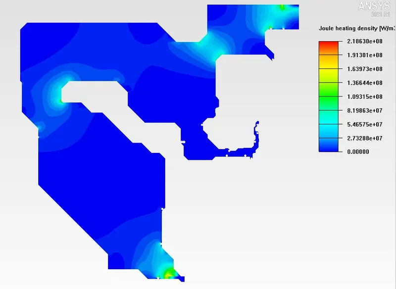
- Joule heating Contour at the Selected Solid Trace of the PCB -
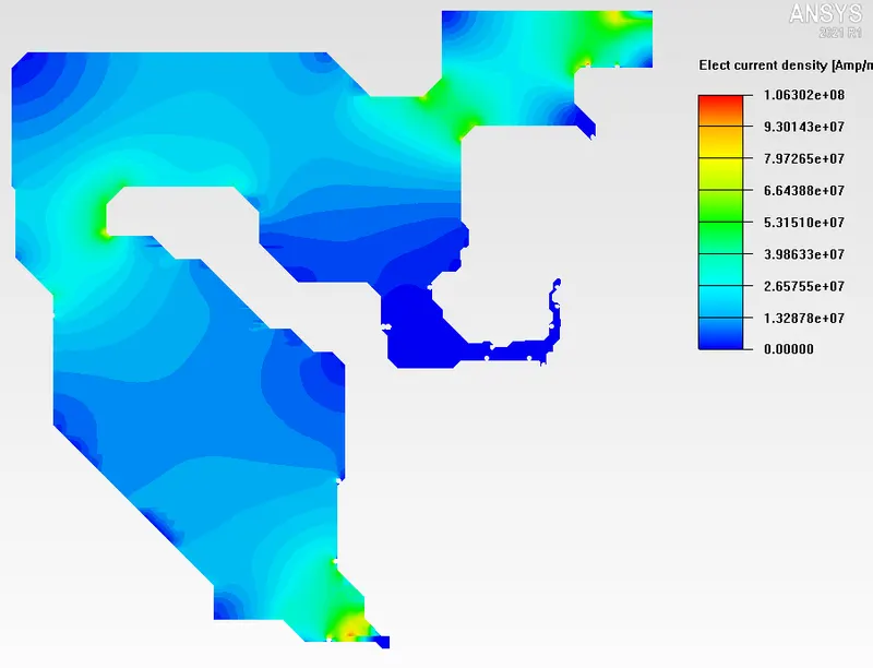
- Electric Current Density at the Selected Solid Trace of the PCB
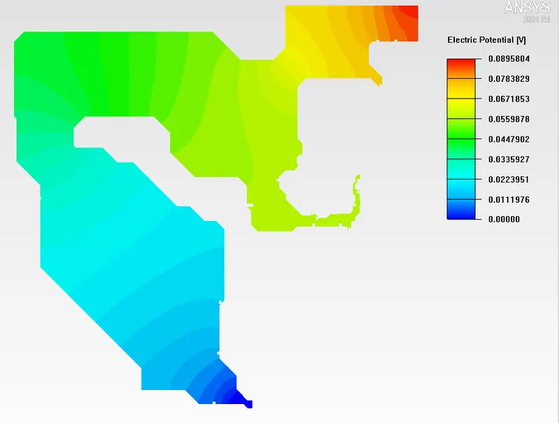
- Electric Potential Contour at the Selected Solid Trace of the PCB
CONCLUSION :
We have successfully performed the simulation analysis of the PCB Electronic System, by importing the given geometry and suitable meshing.
The solver was set up using suitable settings to incorporate the following physical phenomena: Forced convection, Joule heating, Trace Heating.
We were able to generate required contours for temperature, speed, thermal conductivity, electrical potential,etc.
The following are the outcomes of the simulations :
i) Thermal conductivity Analysis of the PCB
- We simulated the PCB board just for Thermal Conduction inorder to see the thermal conductivity of the PCB.
- We were able to see metal fractions of the different layers of the PCB. And also able to find and plot inplane and normal Conductivity of the PCB.
ii) Simulating Forced Convection Cooling of the Whole PCB model with Components
- In this analysis, we simulated the PCB cooling by forced convection with all necessary components attached.
- Maximum temperature within the computational domain is Appx. 168 Deg.C
- Maximum air velocity within the computational domain is Appx. 6.16 m/s.
- All the residuals were less than 10e-3. However the accuracy of the analysis can be improved by refining the mesh.
- We were able visualize the temperature, thermal conductivity and velocity contours of the analysis.
iii) Simulating Forced Convection Cooling of the PCB model with the trace Heating
- In this analysis, the case system was same as the previous once, but with a PCB trace to be analysed for Joule heating and Heat transfer.
- In this, the meshing has been more refined than previous version inorder for better accuracy.
- Maximum temperature within the computational domain is Appx. 81 Deg.C
- Maximum air velocity within the computational domain is Appx. 8.65 m/s.
- The temperatures attained in this version seems realistic and all the residuals are less than 10e-3.
- We were able visualize the temperature, thermal conductivity and velocity contours of the analysis, also plotted the contours for the selected & analysed trace in PCB.