Week-7 Challenge: DC Motor Control
1. A. Explain a MATLAB demo model named ‘Speed control of a DC motor using BJT H-bridge’.
B. Comment on the armature current shoot-up from the scope results.
C. Refer to the help section of ‘The Four-Quadrant Chopper DC Drive (DC7) block’. Compare it with the H-bridge model.
2. Develop a 2-quadrant chopper using simulink & explain the working of the same with the relevant results. (Refer to article - Multiquadrant operation of motor )
3. Explain in a brief about operation of BLDC motor.
1.
BJT:
Construction
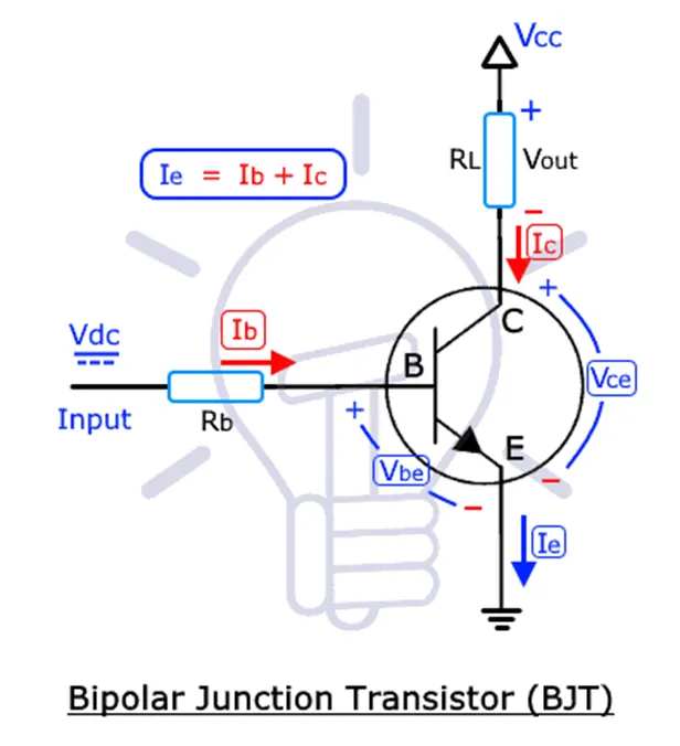
Bipolar junction transistor is formed by the combination of two back-to-back doped semiconductor materials. In other words, BJT is formed by the “sandwich” of back to back extrinsic semiconductor materials. These extrinsic semiconductors are PN junction diodes. Two PN junctions’ diodes are sandwiched together to form a three-terminal device known as BJT transistor. BJT is a three-terminal device having two junctions.
After doping an intrinsic semiconductor with Trivalent or Pentavalent impurities a P-type semiconductor or N-type semiconductor respectively is made. If the number of electrons are greater than the number of holes (positive carriers) then that is known as N-type semiconductor material. While in P-type semiconductor, the number of holes is greater than the number of electrons. When P-type and N-type material are connected together then it becomes a PN-junction diode. BJT transistors are formed after connecting two PN junctions back-to-back. These transistors are known as PNP or NPN bipolar junction transistors depending on whether P or N-type is sandwiched.
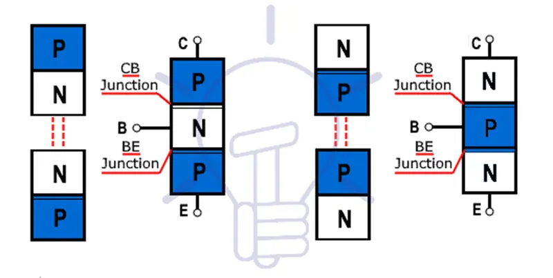
Basically, transistors have three portions and two junctions. These three portions are called Emitter, Collector, and Base. The emitter and collector sandwich the base in between them. The middle portion (base) forms two junctions with the emitter & collector. The junction of the base with emitter is known as the Emitter-Base junction while the junction of the base with the collector is known as the Collector-Base junction.
Terminals of BJT
There are three terminals of BJT. These terminals are knowns as collector, emitter and base.
Emitter
The emitter is the portion on one side of the transistor which emits electrons or holes to the other two portions. The base is always reverse bias with respect to emitter so that it can emit a large number of majority carriers. It is the most heavily doped region of the BJT. The emitter-base junction should be always forward bias in both PNP and NPN transistors. Emitter supplies electrons to the emitter-base junction in NPN while it supplies holes into the same junction in PNP transistor.
Collector
The portion on the opposite side of the Emitter that collects the emitted charge carriers (i.e., electrons or holes) is known as collector. The collector is heavily doped but the doping level of the collector is in between the lightly doping level of base and heavily doped level of emitter. Collector-base junction should be always reversed biased in both PNP and NPN transistors. The reason for reverse biasing is to remove charge carriers (electrons or holes) from the collector-base junction. The collector of NPN transistor collects electrons emitted by emitter. While in PNP transistor, it collects holes emitted by emitter.
Base
The base is the middle portion between collector and emitter & it forms two PN junctions between them. The base is the most lightly doped portion of the BJT. Being the middle portion of the BJT allows it to control the flow of charge carriers between emitter and collector. The base-collector junction shows high resistance because this junction is reversed bias.
Type of BJT
This three-layer device formed by back to back connection has specific names. It can be weather PNP or NPN. Both connections are disused here briefly.
PNP Construction
In PNP bipolar transistor, the N-type semiconductor is sandwiched between two P-type semiconductors. PNP transistors can be formed by connecting cathodes of two diodes. The cathodes of the diodes are connected together at a common point known as base. While the anodes of the diodes that are on the opposite sides are known as the collector and the emitter.
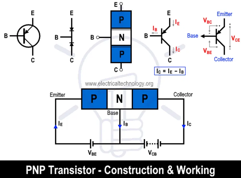
The emitter-base junction is forward bias while collector-base junction is reverse bias. So, in PNP type current flows from emitter to collector. The emitter, in this case, is at high potential to both collector and base.
NPN Construction
NPN type is exactly opposite to PNP type. In NPN bipolar transistor, the P-type semiconductor is sandwiched between two N-type semiconductors. When the anodes of two diodes are connected together it forms an NPN transistor. The current will flow from the collector to emitter because the collector terminal is more positive than emitter in NPN connection.
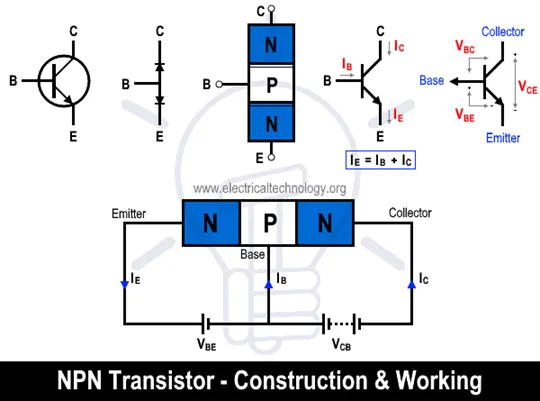
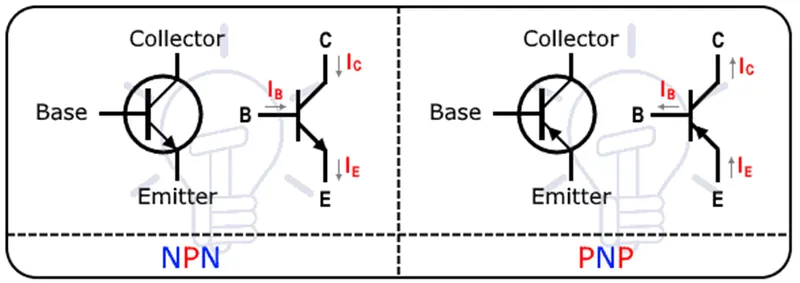
The difference between PNP and NPN symbol is the arrow mark at the emitter which shows the direction of flow of current. The current will either flow from emitter to collector or from collector to emitter. The arrow mark in PNP transistor is inward, which shows the flow of current from emitter to collector. In case of NPN collector, the arrow mark is outward, which shows the flow of current from collector to emitter.
Working of BJT
The word “transistor” is the combination of two words, “Trans” (Transform) and “istor” (Varistor). So, it means the transistor can transform its resistance. The resistance varies in such way that it can either act as an insulator or conductor by applying small signal voltage. This changing ability makes it able to perform both as an “Amplifier” or a “Switch”. It can be used either as a switch or an amplifier at a single time. Therefore, BJT can operate in three different regions to perform the said operation.
Active Region:
In Active region, one of the junctions is in a forward bias while the other is in reverse bias. Here, the base current Ib can be used to control the amount of collector current Ic. Therefore, the active region is used for amplification purposes where the BJT acts as an amplifier with a gain β using the equation;
ic = β x Ib
It is also known as linear region. This region is in between the cutoff region and the saturation region. The normal operation of BJT occurs in this region.
Saturation Region:
In saturation region, both of the junctions of the BJT are in forward bias. This region is used for the ON-state of a switch where;
ic = isat
Isat is the saturation current & it is the maximum amount of current flowing between emitter and collector when BJT is in saturation region. Since both junctions are in forward bias so, BJT acts as a short circuit.
Cutoff Region:
In cutoff region, both junctions of a BJT are in reverse bias. Here the BJT work as off state of a switch where
ic = 0
The operation in this region is completely opposite to the saturation region. There are no external supplies connected. There’s no collector current and hence no emitter current. In this mode, transistor acts as an off-state of the switch. This mode is achieved by reducing base voltage less than both emitter and collector voltage.
Working Principle of BJT
BJT have two junctions formed by the combination of two back to back PN junctions. Base-Emitter junction (BE) is forward bias while collector-emitter junction (CE) is reverse bias. At BE junction, the potential barrier decreases with forward bias. So, electron start flowing from emitter terminal to base terminal. As the base is lightly doped terminal, so very little number of electrons from emitter terminal combine with holes in base terminal. Due to combination of electrons and holes, current from base terminal will start flowing known as Base current (ib). Base current is only 2% of the emitter current Ie while the remaining electrons will flow from the reverse bias collector junction known as Collector current (ic). The total emitter current will be the combination of base current & collector current given by;
ie = ib+ic
Where ie is approximately equal to ic because Ib is almost 2% of the IC.
IGBT:
The Insulated Gate Bipolar Transistor also called an IGBT for short, is something of a cross between a conventional Bipolar Junction Transistor, (BJT) and a Field Effect Transistor, (MOSFET) making it ideal as a semiconductor switching device.
The IGBT Transistor takes the best parts of these two types of common transistors, the high input impedance and high switching speeds of a MOSFET with the low saturation voltage of a bipolar transistor, and combines them together to produce another type of transistor switching device that is capable of handling large collector-emitter currents with virtually zero gate current drive.
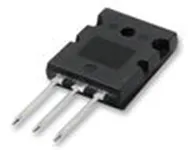
The Insulated Gate Bipolar Transistor, (IGBT) combines the insulated gate (hence the first part of its name) technology of the MOSFET with the output performance characteristics of a conventional bipolar transistor, (hence the second part of its name).
The result of this hybrid combination is that the “IGBT Transistor” has the output switching and conduction characteristics of a bipolar transistor but is voltage-controlled like a MOSFET.
IGBTs are mainly used in power electronics applications, such as inverters, converters and power supplies, were the demands of the solid state switching device are not fully met by power bipolars and power MOSFETs. High-current and high-voltage bipolars are available, but their switching speeds are slow, while power MOSFETs may have higher switching speeds, but high-voltage and high-current devices are expensive and hard to achieve.
The advantage gained by the insulated gate bipolar transistor device over a BJT or MOSFET is that it offers greater power gain than the standard bipolar type transistor combined with the higher voltage operation and lower input losses of the MOSFET. In effect it is an FET integrated with a bipolar transistor in a form of Darlington type configuration as shown.
Insulated Gate Bipolar Transistor
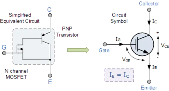
We can see that the insulated gate bipolar transistor is a three terminal, transconductance device that combines an insulated gate N-channel MOSFET input with a PNP bipolar transistor output connected in a type of Darlington configuration.
As a result the terminals are labelled as: Collector, Emitter and Gate. Two of its terminals (C-E) are associated with the conductance path which passes current, while its third terminal (G) controls the device.
The amount of amplification achieved by the insulated gate bipolar transistor is a ratio between its output signal and its input signal. For a conventional bipolar junction transistor, (BJT) the amount of gain is approximately equal to the ratio of the output current to the input current, called Beta.
For a metal oxide semiconductor field effect transistor or MOSFET, there is no input current as the gate is isolated from the main current carrying channel. Therefore, an FET’s gain is equal to the ratio of output current change to input voltage change, making it a transconductance device and this is also true of the IGBT. Then we can treat the IGBT as a power BJT whose base current is provided by a MOSFET.
The Insulated Gate Bipolar Transistor can be used in small signal amplifier circuits in much the same way as the BJT or MOSFET type transistors. But as the IGBT combines the low conduction loss of a BJT with the high switching speed of a power MOSFET an optimal solid state switch exists which is ideal for use in power electronics applications.
Also, the IGBT has a much lower “on-state” resistance, RON than an equivalent MOSFET. This means that the I2R drop across the bipolar output structure for a given switching current is much lower. The forward blocking operation of the IGBT transistor is identical to a power MOSFET.
When used as static controlled switch, the insulated gate bipolar transistor has voltage and current ratings similar to that of the bipolar transistor. However, the presence of an isolated gate in an IGBT makes it a lot simpler to drive than the BJT as much less drive power is needed.
An insulated gate bipolar transistor is simply turned “ON” or “OFF” by activating and deactivating its Gate terminal. Applying a positive input voltage signal across the Gate and the Emitter will keep the device in its “ON” state, while making the input gate signal zero or slightly negative will cause it to turn “OFF” in much the same way as a bipolar transistor or eMOSFET. Another advantage of the IGBT is that it has a much lower on-state channel resistance than a standard MOSFET.
IGBT Characteristics
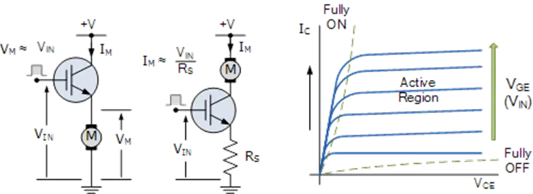
Because the IGBT is a voltage-controlled device, it only requires a small voltage on the Gate to maintain conduction through the device unlike BJT’s which require that the Base current is continuously supplied in a sufficient enough quantity to maintain saturation.
Also the IGBT is a unidirectional device, meaning it can only switch current in the “forward direction”, that is from Collector to Emitter unlike MOSFET’s which have bi-directional current switching capabilities (controlled in the forward direction and uncontrolled in the reverse direction).
The principal of operation and Gate drive circuits for the insulated gate bipolar transistor are very similar to that of the N-channel power MOSFET. The basic difference is that the resistance offered by the main conducting channel when current flows through the device in its “ON” state is very much smaller in the IGBT. Because of this, the current ratings are much higher when compared with an equivalent power MOSFET.
The main advantages of using the Insulated Gate Bipolar Transistor over other types of transistor devices are its high voltage capability, low ON-resistance, ease of drive, relatively fast switching speeds and combined with zero gate drive current makes it a good choice for moderate speed, high voltage applications such as in pulse-width modulated (PWM), variable speed control, switch-mode power supplies or solar powered DC-AC inverter and frequency converter applications operating in the hundreds of kilohertz range.
H-bridge:
In general an H-bridge is a rather simple circuit, containing four switching element, with the load at the center, in an H-like configuration.
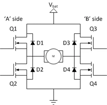
The switching elements (Q1,Q4) are usually bi-polar or FET transistors, in some high-voltage applications IGBTs. Integrated solutions also exist but whether the switching elements are integrated with their control circuits or not is not relevant for the most part for this discussion. The diodes (D1,D4) are called catch diodes and are usually of a Schottky type.
The top-end of the bridge is connected to a power supply (battery for example) and the bottom-end is grounded.
In general all four switching elements can be turned on and off independently, though there are some obvious restrictions.
Though the load can in theory be anything you want, by far the most pervasive application if H-bridges is with a brushed DC or bipolar stepper motor (steppers need two H-bridges per motor) load. In the following I will concentrate on applications as a brushed DC motor driver.
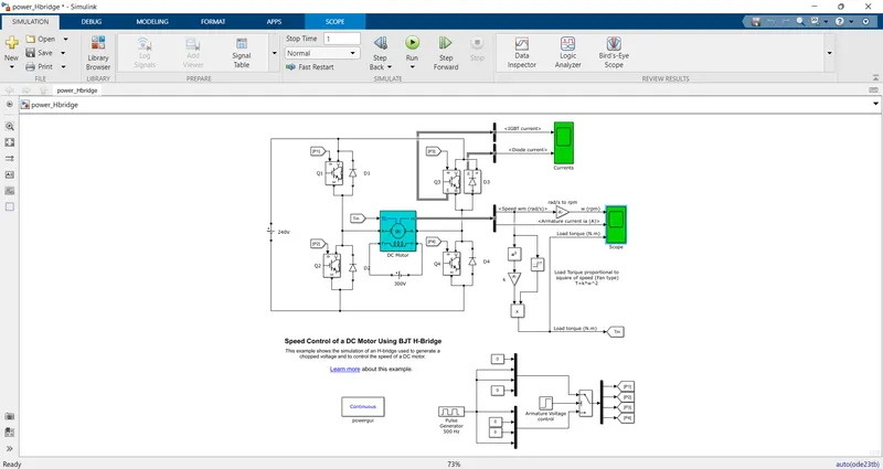
1 (a) Speed control of a DC motor using BJT H-bridge’.
*Open the matlab and type a command as power_Hbridge and then run the command then openning the demo model of speed control of a dc motor using BJT H-bridge then simulation will open the model is shown below
operation:
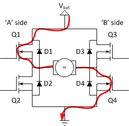
The basic operating mode of an H-bridge is fairly simple: if Q1 and Q4 are turned on, the left lead of the motor will be connected to the power supply, while the right lead is connected to ground. Current starts flowing through the motor which energizes the motor in (let’s say) the forward direction and the motor shaft starts spinning.
If Q2 and Q3 are turned on, the reverse will happen, the motor gets energized in the reverse direction, and the shaft will start spinning backwards.
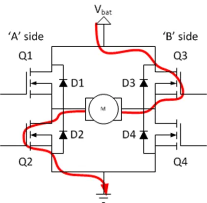
In a bridge, you should never ever close both Q1 and Q2 (or Q3 and Q4) at the same time. If you did that, you just have created a really low-resistance path between power and GND, effectively short-circuiting your power supply. This condition is called ‘shoot-through’ and is an almost guaranteed way to quickly destroy your bridge, or something else in your circuit.
From the demo model the igbt switch is controlled by simulink signal that is 1 or 0.
The DC motor uses the preset model (5 HP 24V 1750 rpm). It simulates a fan type load (where Load torque is proportional to square of speed). The armature mean voltage can be varied from 0 to 240 V when the duty cycle (specified in the Pulse Generator block) is varied from 0 to 100%.
The demo model is run for 1 sec with default values
Total cycle time=1 second
duty cycle=75%
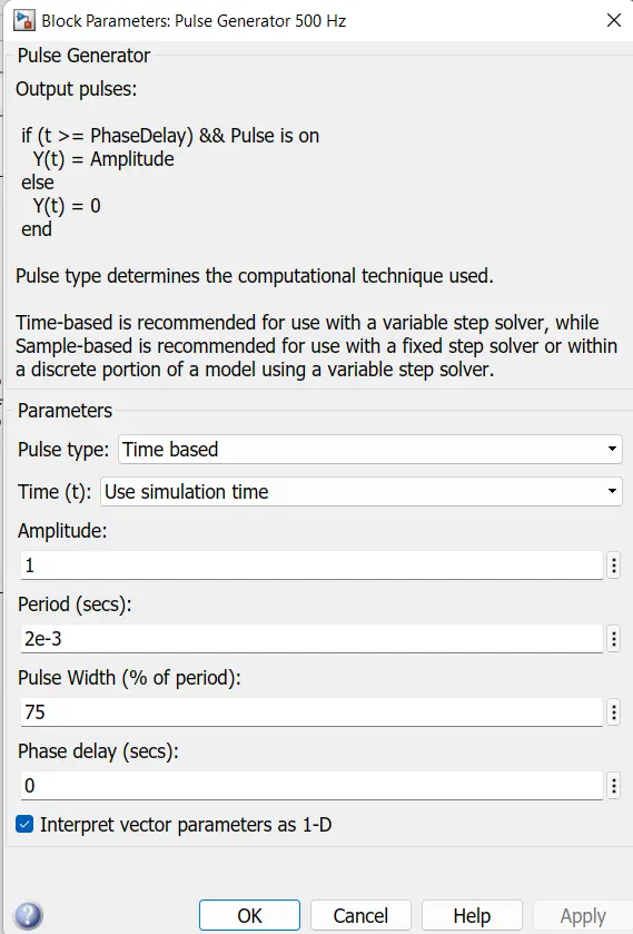
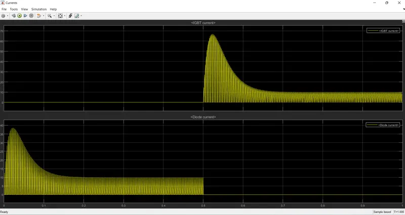
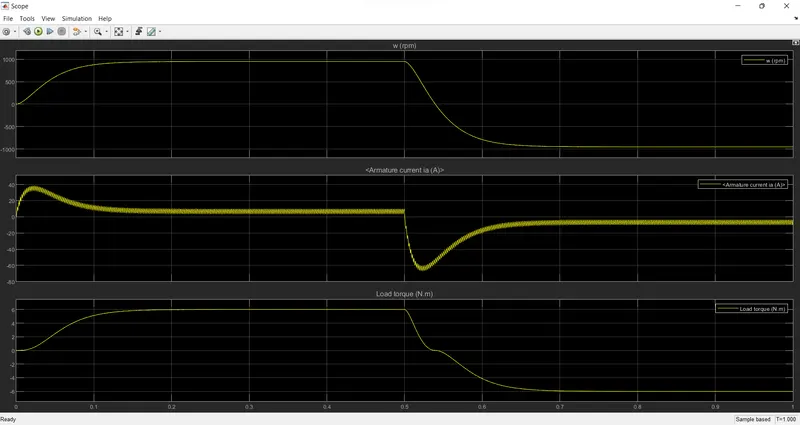
After run the simulation results are came that are shown below
1(b) Comment on the armature current shoot-up from the scope results.
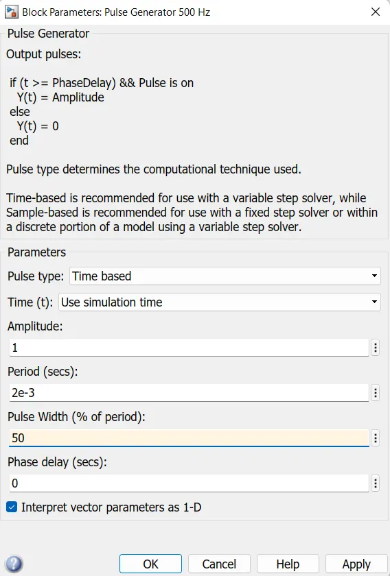
In the demo model pulse generator is used to change the input values of duty cycle and amplitude ,according to the input values signal is generated and given to the switches. the above demo model is run a cycle of 1sec and duty cycle is reduced to 50% and remaining parameters are same then the reslts are as follow.
Case-1
duty cycle=50%
From 0 to 0.5sec the IGBT switches Q1 & Q4 are conducted and the Q2 & Q3 are turned off in this condition the motor will run forward or clockwise direction.
From 0.5 to 1sec the IGBT switches Q2 & Q3 are conducted and the Q1 & Q4 are turned off in this condition the motor will run reverse or anti-clockwise direction
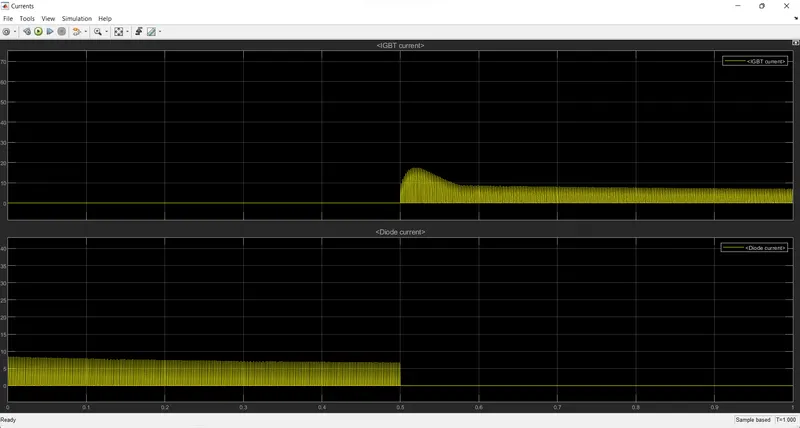
from the above plot we can observe the diode current is shoot up after 0.5sec and 0 to 0.5 sec their is no shoot up for diode current.
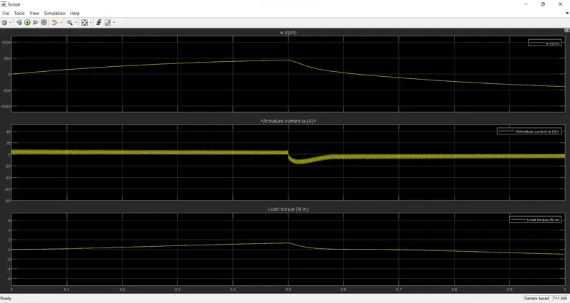
Above plot shows armature current,speed & load torque.
Case-2
Duty cycle=30%
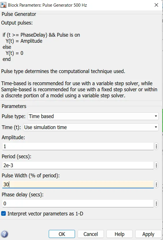
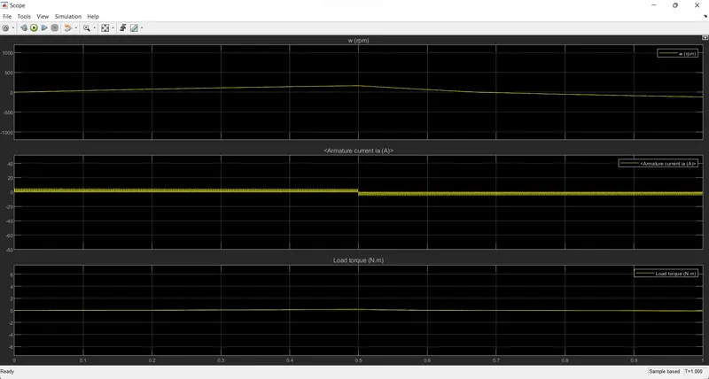
For reducing duty cycle the armature current is shoot up After 0.5sec and also constant at 5A positive and nagative cycle.
1(c) The Four-Quadrant Chopper DC Drive (DC7) block. Compare it with the H-bridge model.
A four-quadrant chopper is a chopper which can operated in all the four quadrants. The power can flow either from source to load or load to source in this chopper. In first quadrant, a Class-E chopper acts as a step-down chopper whereas in second quadrant it behaves as a step-down chopper. This type of chopper is also known as Class-E or Type-E chopper.
Working Principle / Operation of Class-E Chopper:
The circuit of a four-quadrant chopper or class-E chopper basically consists of four semiconductor switches CH1 to CH4 and four Diodes D1 to D4. The four diodes are connected in anti-parallel. The circuit diagram of this type of chopper is shown below.
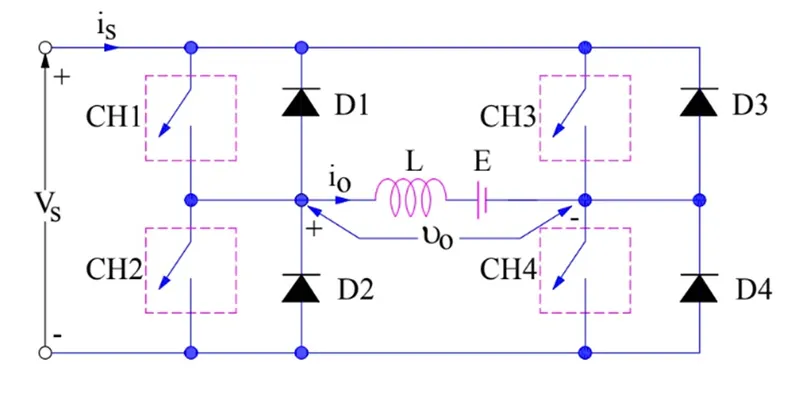
In the above circuit diagram, the choppers are numbered CH1 to CH4. For first quadrant operation CH1 is made ON, for second quadrant operation CH2 is made ON and so on. To better understand the working of four quadrant chopper, we will discuss its operation separately for each quadrant.
Four qudrant chopper simulink model is shown below
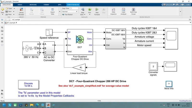
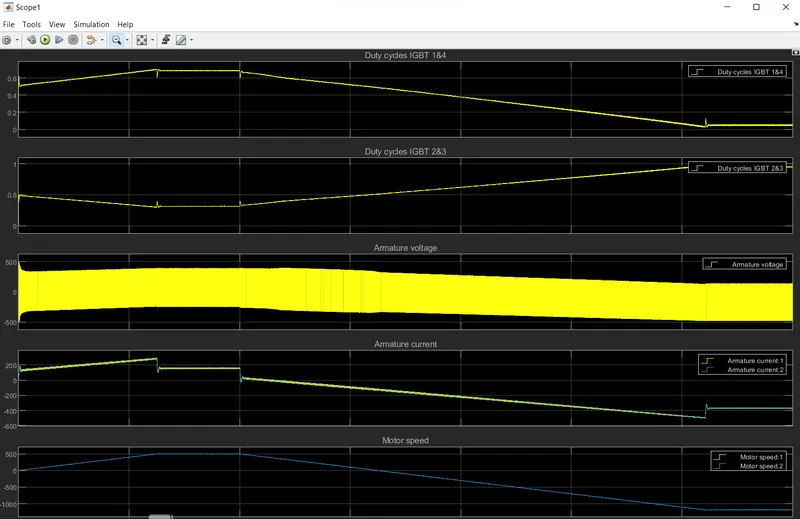
The 200 HP DC motor is separately excited with a constant 150 V DC field voltage source. The armature voltage is provided by an IGBT converter controlled by two PI regulators. The converter is fed by a 515 V DC bus obtained by rectification of a 380 V AC 50 Hz voltage source. In order to limit the DC bus voltage during dynamic braking mode, a braking chopper has been added between the diode rectifier and the DC7 block.
The first regulator is a speed regulator, followed by a current regulator. The speed regulator outputs the armature current reference (in p.u.) used by the current controller in order to obtain the electromagnetic torque needed to reach the desired speed. The speed reference change rate follows acceleration and deceleration ramps in order to avoid sudden reference changes that could cause armature over-current and destabilize the system. The current regulator controls the armature current by computing the appropriate duty ratios of the 5 kHz pulses of the four IGBT devices (Pulse Width Modulation). For proper system behaviour, the instantaneous pulse values of IGBT devices 1 and 4 are opposite to those of IGBT devices 2 and 3. This generates the average armature voltage needed to obtain the desired armature current. In order to limit the amplitude of the current oscillations, a smoothing inductance is placed in series with the armature circuit.
First Quadrant Operation:
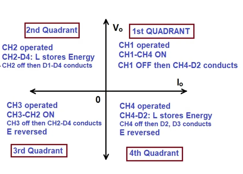
For first quadrant operation, CH4 is kept ON, CH3 is kept OFF and CH1 is operated. When both CH1 & CH4 are ON simultaneously, the load gets directly connected to the source and hence the output voltage becomes equal to the source voltage. This essentially means that vo = vs. It may be noted that the load current flows from source to load as shown by the direction of io.
When CH1 is switched OFF, the load current free wheels through CH4 and D2. During this period, the load voltage and current remains positive.
Thus, both the output voltage vs and load current io are positive and hence, the operation of chopper is in first quadrant. It may be noted that, Class-E chopper operates as a step-down chopper in this case.
Second Quadrant Operation:
To obtain second quadrant operation, CH2 is operated while keeping the CH1, CH3 & CH4 OFF. When CH2 is ON, the DC source in the load drives current through CH2, D4, E and L. Inductor L stores energy during the On period of CH2.
When CH2 is turned OFF, current is fed back to the source through D1, D4. It should be noted at this point that (E+Ldi/dt) is more than the source voltage Vs. As load voltage Vo is positive and Io is negative, it is second quadrant operation of chopper. Since, the current is fed back to the source, this simply means that load is transferring power to the source. Kindly read Step-up chopper for detailed analysis and better understanding.
For second quadrant operation, load must contain emf E as shown in the circuit diagram. In second quadrant, configuration operates as a step-up chopper.
Third Quadrant Operation:
To obtain third quadrant operation, both the load voltage and load current should be negative. The current and voltage are assumed positive if their direction matches with what shown in the circuit diagram. If the direction is opposite to what shown in the circuit diagram, it is considered negative. One important thing to notice is that the polarity of emf E in load must be reversed to have third quadrant operation. Circuit diagram of Class-E chopper for third quadrant operation is shown below.
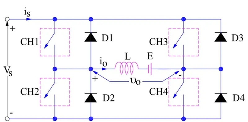
For third quadrant operation, CH1 is kept off, CH2 is kept ON and CH3 is operated. When CH3 is ON, load gets connected to source and hence load voltage is equal to source voltage. But carefully observe that the polarity of load voltage vo is opposite to what shown in the circuit diagram. Hence, vo is assumed negative. Let us now see what is the status of load current io. It may be seen that io is flowing in the direction opposite to shown in the circuit diagram and hence negative.
Now, when CH3 is turned OFF, the negative load current free wheels through the CH2 and D4. In this manner, vo and io both are negative. Hence, the chopper operates in third quadrant.
Fourth Quadrant Operation:
To obtain fourth quadrant operation, CH4 is operated while keeping CH1, CH2 and CH3 OFF. The polarity of load emf E needs to be reversed in this case too like third quadrant operation.
When CH4 is turned ON, positive current flows through CH4, D2, L and E. inductance L stores energy during the time CH4 is ON. When CH4 is made OFF, current is fed back to the source through diodes D2, D3. Here load voltage is negative but the load current is always positive. This leads to chopper operation in fourth quadrant. Here, power is fed back to the source from load and chopper acts as a step-up chopper.
The operation of a four- quadrant chopper or Class-E chopper is summarized in the figure below.
Simulation relusts are shown below
Comparison of H- bridge vs Four quadrant chopper
- Four-Quadrant Chopper can operates in all four modes (Forward Motoring, Forward Braking, Reverse Motoring and Reverse Braking), but H-bridge can operate only in two modes (Forward and Reverse).
- In Four-Quadrant Chopper Regenerative Braking is possible, but H-bridge Regenerative Braking is not
- In Four-Quadrant Chopper Two PI regulator (Speed Regulator and Current Regulator) is used to obtain electromagnetic torque needed to reach the desired speed and control the armature current and stabilize the system, but in H-bridge model PI regulator is not
- H-bridge is an electronic circuit that switches the polarity of voltage applied to the load and Four-quadrant Chopper is electronic switch that is used to interrupt one signal under the control of
- H-bridge circuit is often used in Robotics and other applications to allow dc motor to run forward and backward. Four- Quadrant Chopper circuit is used to refer numerous type of electronic switching devices and circuits used in power control and signal applications
- Four-Quadrant Chopper model gives better efficiency and high energy(power) storage than H-bridge.
2.
Two quadrant chopper:
Class-C or Type-C Chopper is a category of chopper which can operate in first as well as second quadrant. This basically means that, the power can either flow from source to load or load to source in this chopper. This kind of chopper is also known as Two Quadrant Class-A chopper.
As we know that, a Class-A and Chopper-B Choppers operates in first and second quadrant respectively. Therefore, if we connect both these types of choppers in parallel then it is possible to have chopper operation in first as well as second quadrant.
In fact, Class-C or Type-C chopper is obtained by the parallel connection of Class-A and Class-B chopper. Figure below shows the circuit diagram of this type of chopper.
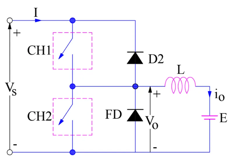
Case-1: When CH1 is switched ON / OFF
When chopper CH1 is switched ON, source Vs directly gets connected to the load and hence, load voltage Vo is equal to source voltage. The direction of load current is from source to load as shown in the circuit diagram which is assumed positive.
When CH1 is switched OFF, the free-wheeling diode FD comes into the circuit as it gets forward biased and hence shorts the load. Therefore, the output voltage Vo becomes zero. However, the io continues to die down through the FD and L in the same direction as shown in circuit diagram. Thus, the average output voltage Vo and current Io are positive and hence operation of chopper is in first quadrant. In fact, this is the Class-B mode of operation.
Case-2: When CH2 is switched ON / OFF
When chopper CH2 is switched ON, load DC source E drives current through CH2 and load. The direction of this current io will be opposite to that shown in circuit diagram and hence is assumed negative. Output voltage Vo is zero during this time. When CH2 is made OFF, diode D2 gets forward biased and hence the current into the source from the load. The output voltage is Vs in this time as the load is connected to the source through D2 during OFF time of chopper CH2. Thus, the load current is always negative i.e. operation of chopper is within second quadrant. In fact, this is the Class-B mode of operation.
From the above two cases, we can conclude the following points:
- The output voltage Vois zero when chopper CH2 is ON or free-wheeling diode FD conducts.
- The output voltage Vois equal to source voltage Vs when chopper CH1 is ON or diode D2 conducts.
- The load current flows in the direction shown in circuit diagram i.e.iois positive when CH1 is ON or FD conducts.
- The load current flows opposite to the direction shown in circuit diagram i.e.iois negative when CH2 is ON or D2 conducts.
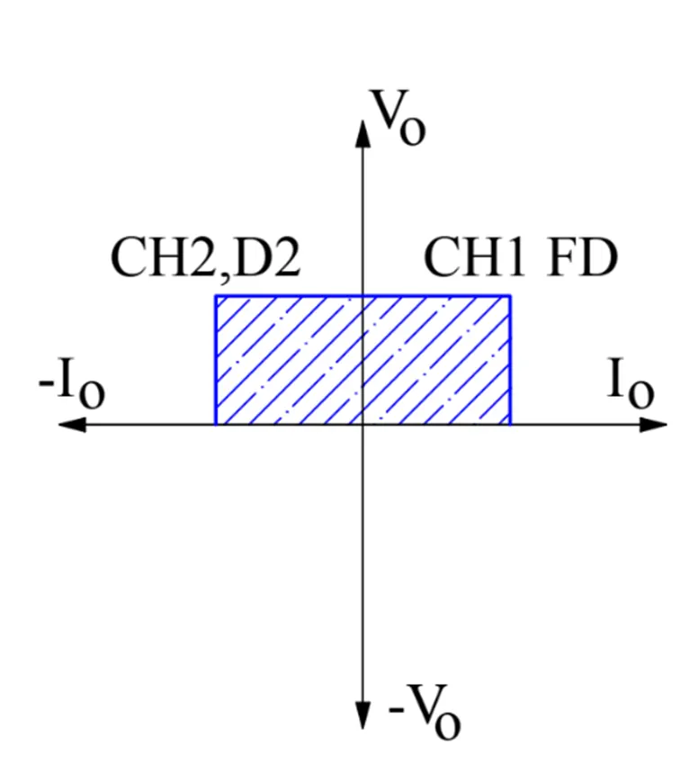
The average load voltage is always positive but the average load current may be positive or negative. Therefore, power flow may be from source to load (first quadrant operation) or load to source (second quadrant operation). The operating region of Class-C or Type-C chopper is shown below by hatched area.
the simulink model of two quadrant chopper is shown below
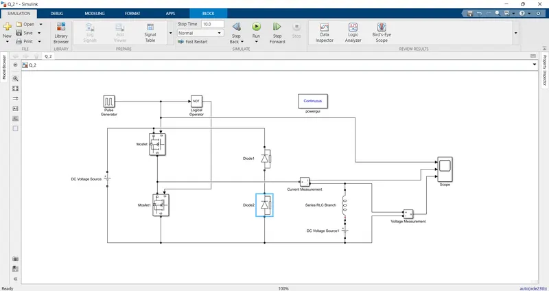
For developing a model i am used some blocks that are shown below
MOSFET:
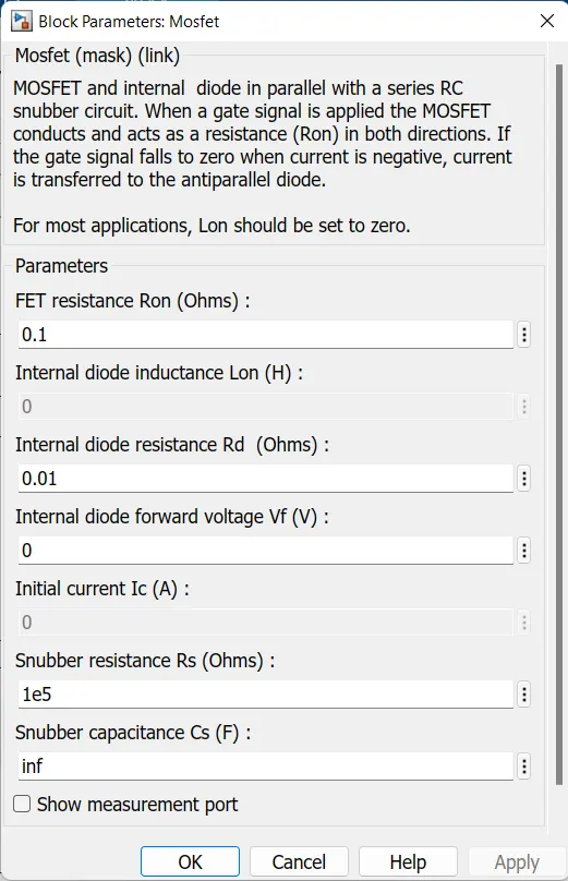
The metal-oxide semiconductor field-effect transistor (MOSFET) is a semiconductor device controllable by the gate signal (g > 0). The MOSFET device is connected in parallel with an internal diode that turns on when the MOSFET device is reverse biased (Vds < 0) and no gate signal is applied (g=0). The model is simulated by an ideal switch controlled by a logical signal (g > 0 or g =0), with a diode connected in parallel.
The MOSFET device turns on when a positive signal is applied at the gate input (g > 0) whether the drain-source voltage is positive or negative. If no signal is applied at the gate input (g=0), only the internal diode conducts when voltage exceeds its forward voltage Vf.
With a positive or negative current flowing through the device, the MOSFET turns off when the gate input becomes 0. If the current I is negative and flowing in the internal diode (no gate signal or g = 0), the switch turns off when the current I becomes 0.
block parameters are shown below
Diode:
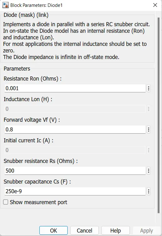
If the diode forward voltage exceeds the value specified in the Forward voltage parameter, the diode behaves as a linear resistor with the resistance specified in the On resistance parameter. Otherwise, the diode behaves as a linear resistor with the small conductance specified in the Off conductance parameter. Zero voltage across the diode results in zero current flowing.
parameters are shown below
logical operator:
Int that operator NOT gate is used for conducting only one switch at time for avoiding the short circuit.
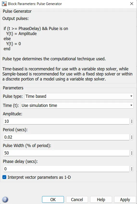
pulse generator:

To generate the signals and send to the switch of the gate signal.
parameter shown below
Dc voltage sources
The main dc voltage source is taken as 48 v as shown below
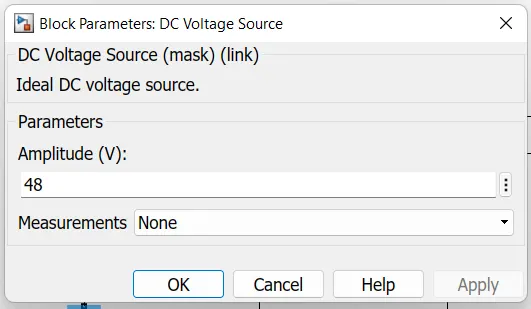
And the load side dc voltage is 24v is shown below
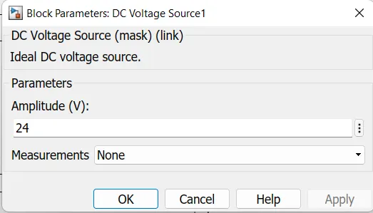
Run the simulation and then getting a results shown below
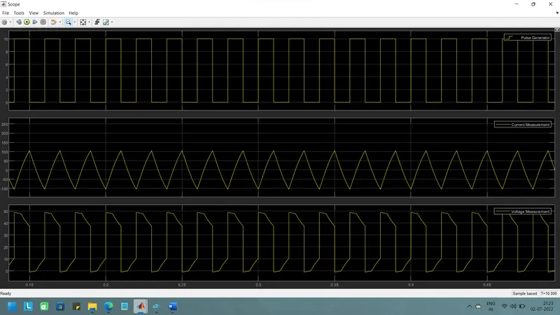
The above plot shows pulse generator,current measurement & voltage measurement.
When the chopper CH1 is switched on source vs directly connected to the load and load voltage vo is equal to source voltage.
The direction of load current is from source to load shown in the circuit diagram get forward biased and hence shorts the load therefore the output voltage vo becomes zero.
when chopper ch2 is switched on loaad dc source E drives current through ch2 and load.
the direction of current direction is opposite as shown circuit diagram.output voltage vo is zero during this time
3.
Operation of BLDC motor:
A Brushless DC Motor is similar to a Brushed DC Motor but as the name suggests, a BLDC doesn’t use brushes for commutation but rather they are electronically commutated. In conventional Brushed DC Motors, the brushes are used to transmit the power to the rotor as they turn in a fixed magnetic field.
As mentioned earlier, a BLDC motor used electronic commutation and thus eliminates the mechanically torn brushes.
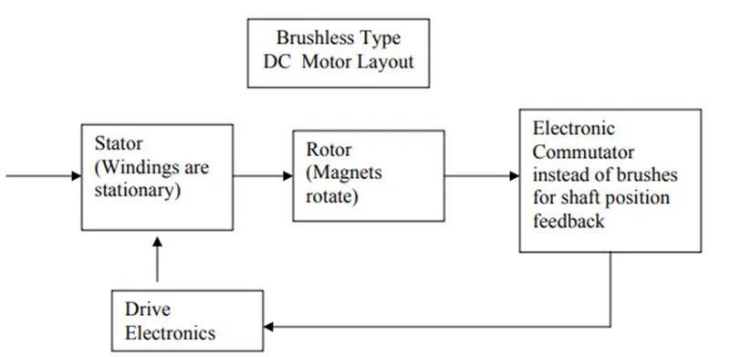
Construction Of A BLDC Motor
A commutator-brushes arrangement helps in achieving unidirectional torque in a typical Dc motor. Obviously, commutator and brush arrangement is eliminated in a brushless dc motor. Here, an integrated inverter/switching circuit is used to achieve unidirectional torque. That is why these motors are, sometimes, also referred as 'electronically commutated motors'.
Just like any other electric motor, a BLDC motor also consists of two main parts a stator and a rotor. Permanent magnets are mounted on the rotor of a BLDC motor, and the stator is wound for a specific number of poles. Also, a control circuit is connected to the stator winding. Most of the times, the inverter/control circuit or controller is integrated into the stator assembly. This is the basic constructional difference between a brushless motor and a typical dc motor.
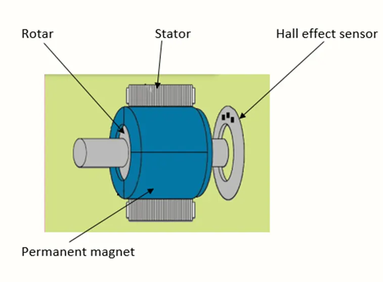
A typical controller provides a three-phase frequency-controlled supply to the stator winding. The supply is controlled by logical control circuits and energizes specific stator poles at a specific point of time. This can be understood from the below animations about working of BLDC motors.
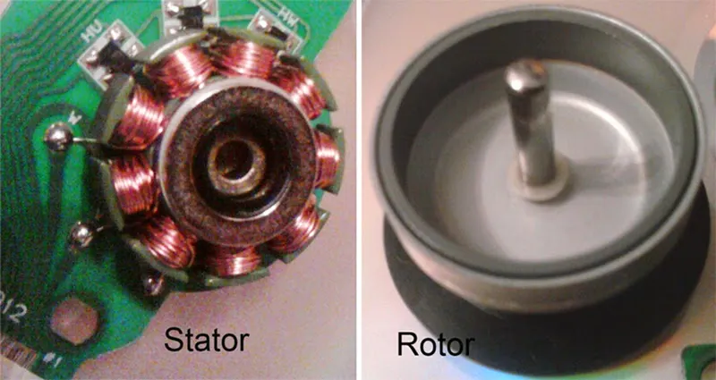
There are two types of BLDC motors based on their construction/design: (i) inner rotor design & (ii) outer rotor design. Regardless of these types, note that the permanent magnets are always mounted on the rotor and winding on the stator.
1.Inner rotor design (inrunner): this is a conventional design, where the rotor is located at the core (center) and stator winding surrounds it.
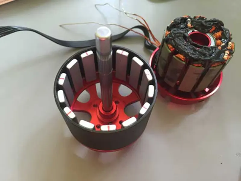
2.Outer rotor design (outrunner): In this configuration, the rotor is external. i.e., stator windings are located at the core while the rotor, carrying permanent magnets, surrounds the stator.
Working Principle and Operation of BLDC Motor
BLDC motor works on the principle similar to that of a conventional DC motor, i.e., the Lorentz force law which states that whenever a current carrying conductor placed in a magnetic field it experiences a force. As a consequence of reaction force, the magnet will experience an equal and opposite force. In case BLDC motor, the current carrying conductor is stationary while the permanent magnet moves.
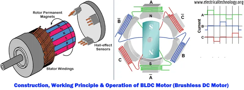
When the stator coils are electrically switched by a supply source, it becomes electromagnet and starts producing the uniform field in the air gap. Though the source of supply is DC, switching makes to generate an AC voltage waveform with trapezoidal shape. Due to the force of interaction between electromagnet stator and permanent magnet rotor, the rotor continues to rotate.
Consider the figure below in which motor stator is excited based on different switching states. With the switching of windings as High and Low signals, corresponding winding energized as North and South poles. The permanent magnet rotor with North and South poles align with stator poles causing motor to rotate.
Observe that motor produces torque because of the development of attraction forces (when North-South or South-North alignment) and repulsion forces (when North-North or South-South alignment). By this way motor moves in a clockwise direction.
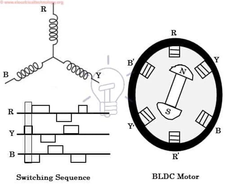
Here, one might get a question that how we know which stator coil should be energized and when to do. This is because; the motor continuous rotation depends on the switching sequence around the coils. As discussed above that Hall sensors give shaft position feedback to the electronic controller unit.
Based on this signal from sensor, the controller decides particular coils to energize. Hall-effect sensors generate Low- and High-level signals whenever rotor poles pass near to it. These signals determine the position of the shaft.
Advantages of BLDC Motor:
Compared with a brushed DC motor or an induction motor, the BLDC motor has many advantages:
- Higher efficiency and reliability
- Lower acoustic noise
- Smaller and lighter
- Greater dynamic response
- Better speed versus torque characteristics
- Higher speed range
- Longer life
Applications of Brushless DC motor
Brushless DC motors (BLDC) use for a wide variety of application requirements such as varying loads, constant loads and positioning applications in the fields of industrial control, automotive, aviation, automation systems, health care equipment’s etc.
- Computer hard drives and DVD/CD players
- Electric vehicles, hybrid vehicles, and electric bicycles
- Industrial robots, CNC machine tools, and simple belt driven systems
- Washing machines, compressors and dryers
- Fans, pumps and blowers.