Project 3
AIM:-
- Creating a workspace for Ethernet shield in altium
- Defining a PCB board size using the DXF data provided
- PCB clearance to be set as 0.15mm and track width to be 0.2mm for power line and 0.15mm for rest of the circuit
- Following the image and BOM provided for creating the schematic and find the datasheet from online for creating the footprint and symbol.
- Use Saturn PCB tool to find the values for 100ohm impedance for the high speed differential pair signals and via current calculation
- Set PCB to 2 layers. Follow the stackup advised on the course module
- Identifying the key points to consider for PCB design using the datasheet
- Assemble and route the components as recommended by the datasheet
- Place the components on top sides of the PCB and tracking on both sides. Use the image as reference to place the components
- Add 4 fiducials as per the image provided diagonally opposite
- PCB board with the text (“Ethernet Shield”)
- Generate 3D files for all the components and a 3D view.
- Generate PCB panel of 150mm x 150mm and place as many circuits as possible and follow routed method v-scoring
- Generate complete output files for DFM and DFA (Gerber, Altium draftsman, X Y data, BOM, assembly diagram, fabrication diagram, PDF’s)
Ethernet shield
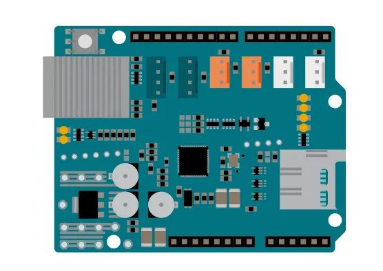
Shematic
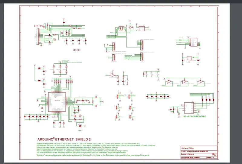
- Creating a workspace for Ethernet shield in altium
STEP 1 CREAT A NEW PROJECT
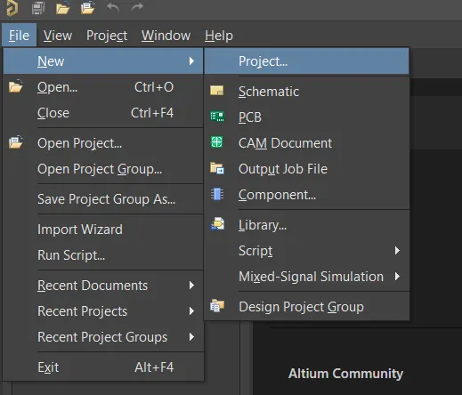
GIVE NAME
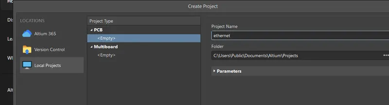
step 2 creat a new schematic library and add name Ethernet
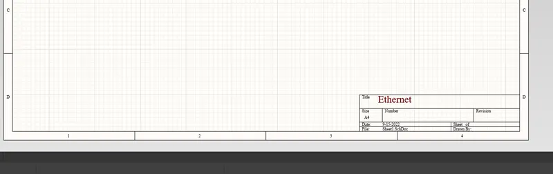
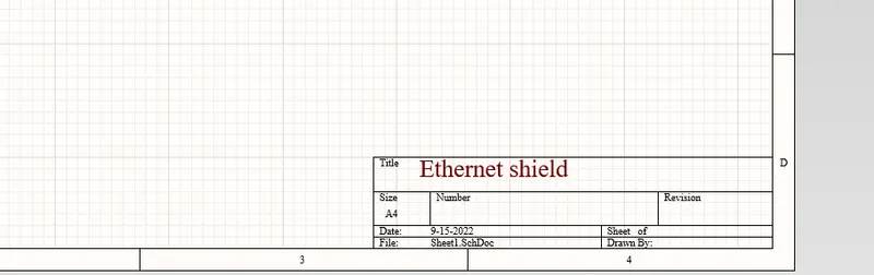
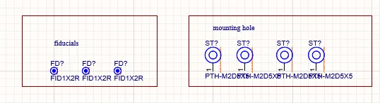
next we need to add fiducials and mounting holes
Fiducials and mounting hole:-
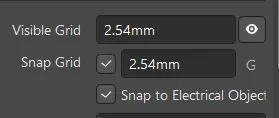
Grid settings:-
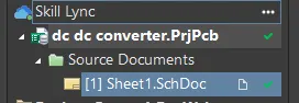
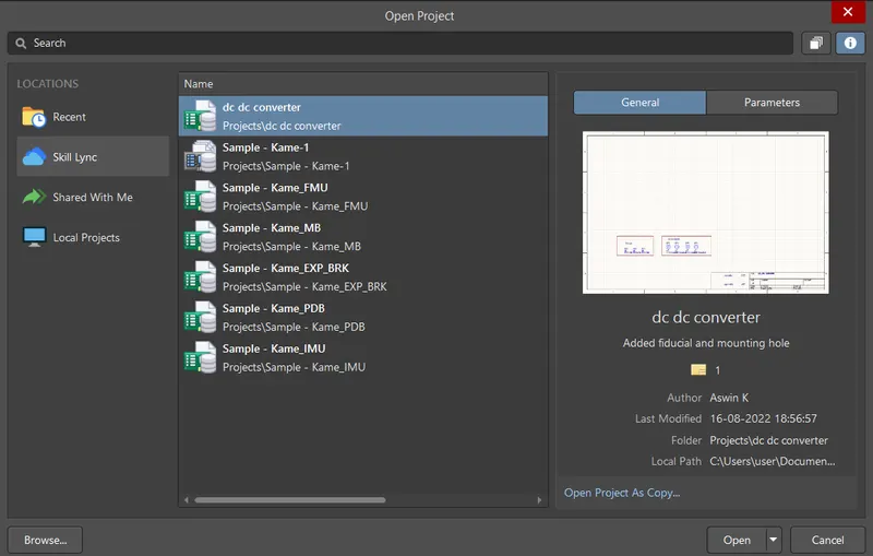
cloud storage result:-
- Defining a PCB board size using the DXF data provided
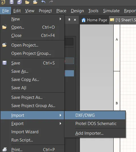
we need make required board line and circuit foot with the help of rules
example.
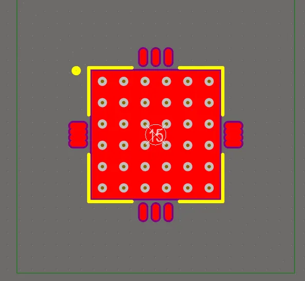
Here i tried PQFN
64 PIN
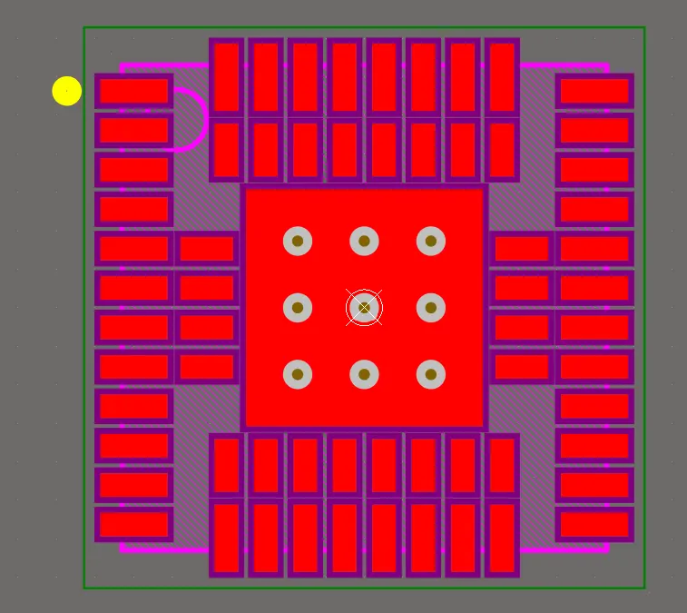
BOARD OUTLINE GIVEN :-
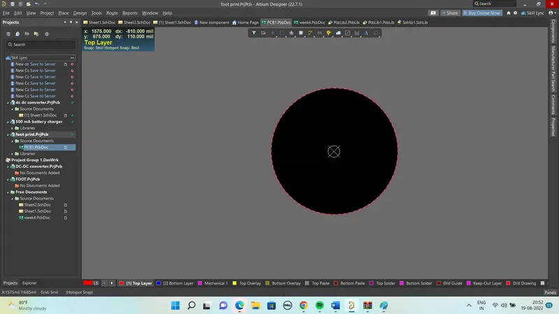
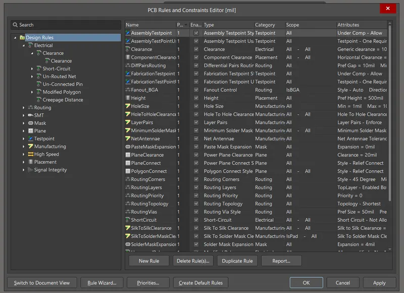
iam gointo design and take rule section
from that all rule give required values and etc...
Routing:-
Finally, we are getting to the part - routing. it’s always exciting to see rapid progress and a project get closer to completion.
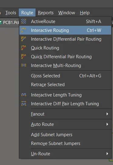
Altium has some fantastic tools that make routing very easy. The Interactive Routing tool is what you’ll most often use for routing. You can get started by pressing Ctrl + W or going to Route → Interactive Routing.
Copper Pours (Polygons)
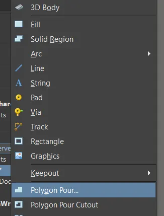
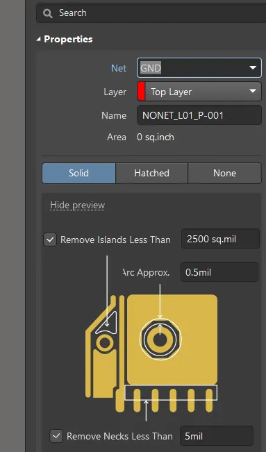
We’re going to add a complete top and bottom copper pour connected to the GND net. This is important for the charger IC's thermal performance, having a copper area to act as a heat sink.
FOLLOWING THE STEP
Thermal relief
Altium PCB design has option to assign the number of thermal spokes as required and has option for the size of the thermal spokes which can also be rotated.
Thermal relief can be applied to specific pin specific net or a components.
it should be direct connection
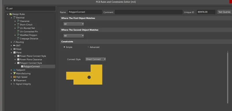
Thermal relief
Altium PCB design has option to assign the number of thermal spokes as required and has option for the size of the thermal spokes which can also be rotated.
Thermal relief can be applied to specific pin specific net or a components.
it should be direct connection
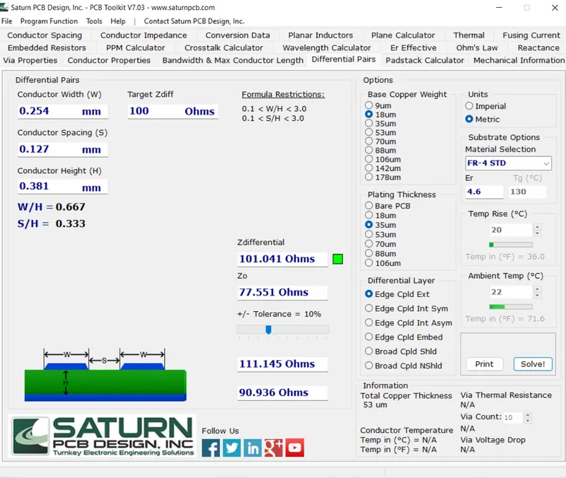
Use Saturn PCB tool to find the values for 100ohm impedance for the high speed differential pair signals and via current calculation
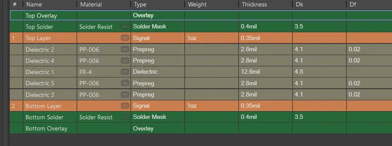
- Set PCB to 2 layers. Follow the stackup advised on the course module
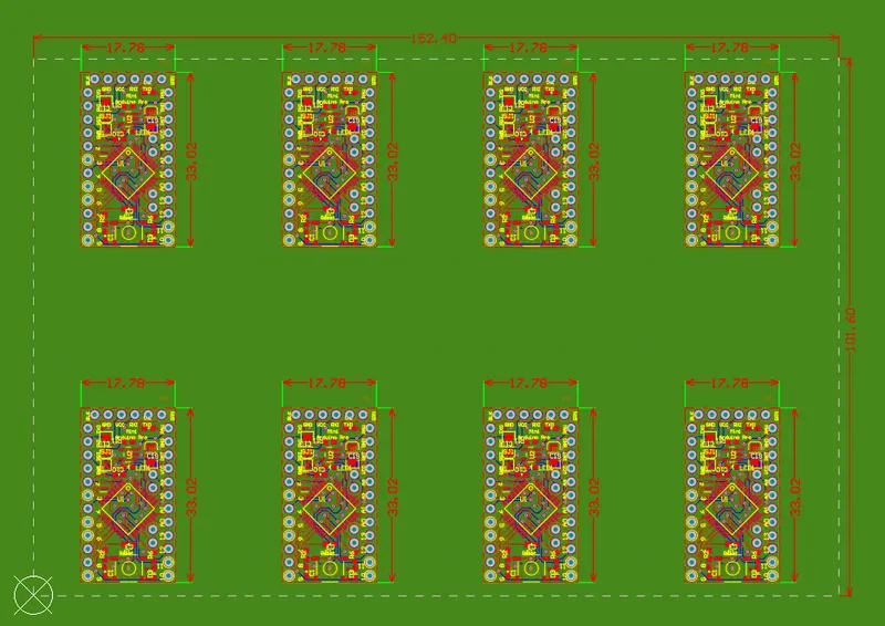
- Generate PCB panel of 150mm x 150mm and place as many circuits as possible and follow routed method v-scoring
example
add new project
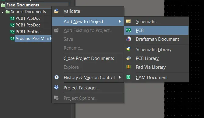
move on next step
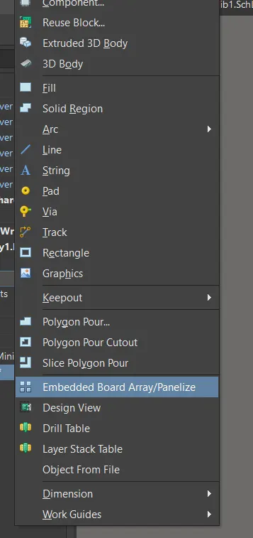
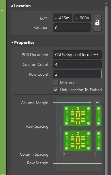
properties:-
so i got
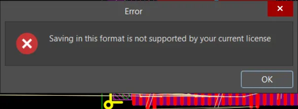
ALTIUM VERSION HAS EXPIRED