Project 2 - SiC/IGBT isolated gate driver reference design with thermal diode and sensing FET
PCB can have single multiple layers of dielectric and conductive materials. These layers when attached with each other, they carry electrical circuits which sometimes linked with each other. According to applications like home electronics, alarm clocks, other household appliances, computers and mobiles. Printed circuit board has also extended its applications with industrial tools and machinery, in most of the medical devices, storage systems and aerospace industry. The number of layers and its dimensions determined by PCB power design.
Five factors are there which are required to be considered before selection of number of layers:
- 1) Applications: It is very important to identify the purpose. Types of machines, complexity of the electronics circuit and power demand.
- 2) Operation frequency:It is also important to determine the operation frequency of the application. Operation frequency of any application indicates the function and the capacity of the printed circuit board. For higher processing speed and capacity a multiple layer PCB is required.
- 3) Economy: Manufacturing cost is another parameter in this list. As the layers are going to increase, so will the cost. If applications required a higher processing speed and capacity then the cost will also escalate.
- 4) Manufacturing time:this talk about the lead time, that means time to manufacture single or multiple layer printed circuit board. This lead time effect all above mentioned parameters.
- 5) Density:The density will also decide the selection of layers. There is another term which is known as pin density. If the pin density is 1, it suggests that printed circuit board must be of single layer. As pin density decreases the number of layers increases. For example; if the value of pin density is 0.2, there is need of at least 10 layers in printed circuit board.
PCB stack up principle:
After the required numbers of layers are determined, the following tasks are required to be completed carefully. So that all circuits are arranged reasonably. There are two required factors:
- Special signal layers distribution.
- Proper distribution of power layer and ground layer.
There could be more possible arrangements for ground layer, power layer and special signal layer as the number of layers. But there are certain principles to make these arrangements of layers:
- 1- The special signal layer should be next to the power layer. Shielded with copper power layer.
- 2- Two avoid the direct contact between two signal layers, a ground layer can be placed between them.
- 3- Multiple ground layer and power layers can reduce impedance effectively.
- 4- The symmetry of layer structure.
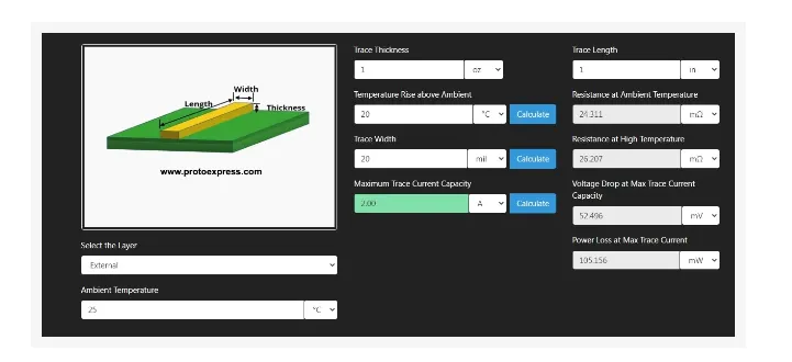
2. To calculate trace width:
PCB - nets - all nets- click the trace required - properties window - width is given
IPC-2221 is generally accepted in electronic industry as a generic PCB design standard. However, when it comes to distances between the PC traces, in my view, the IPC-2221 table 6-1 stepwise limits are mostly baseless: the curve for spacing vs. voltage should be linear. Of course, it is not the only standard that defines the electrical clearance. For power conversion circuits IPC-9592 initial draft provided the following linear circuit board spacing recommendations: SPACING (mm) = 0.6 + Vpeak x .005. In general, a linear relationship makes more sense. However, these requirements were also too conservative and at low voltages were not even practically doable. The updated IPC 9592B document left the above equation only for V≥100V. At other voltages the limits are as following: 0.13mm for V<15V, 0.25mm for 15V≤V<30V and 0.1+Vpeak×0.01 for 30V≤V<100V. Note that all IPC standards are voluntarily rather than mandatory. Conversely, for the products covered by safety standards the creepage and clearance requirements of a respective UL/IEC standard are mandatory. For example, for most ITE applications you need to use UL 60950-1 Tables 2K to 2N.
As a reference, the chart below compares PCB distance limits based on the following three specs for external layers of uncoated bare boards;
- IPC2221B
- IPC9592B;
- UL60950 for functional insulation in secondaries, designed to meet the test per Table 5B with the assumption of 40V/mil withstand voltage.
to calculate trace lenght:
panel - pcb - nets - all nets - click the trace to which lenght is to be calculate - lenght is provided there
Via Sizing Calculations and Charts
Absolute via sizes are not really specified according to industry standards. Instead, only the minimum sizes are specified based on the size of the component that will be mounted on the via. These standards must be followed if your PCB is to be compliant. The IPC-2222 standard specifies minimum hole diameters for plated through-hole vias for different classes of vias as follows:
- Minimum hole size = Maximum lead diameter + 0.25 mm (Level)
- Minimum hole size = Maximum lead diameter + 0.20 mm (Level B)
- Minimum hole size = Maximum lead diameter + 0.15 mm (Level C)
If you’re not familiar with this terminology, the lead diameter refers to the size of pin on a component that will appear on a particular plated through-hole via.
In addition to standard via sizes, there are also standardized pad sizes that should be used in compliant PCBs. The IPC-2221A standard defines minimum pad sizes for vias as a + 2b + c, where a is the maximum hole diameter, minimum annular ring size, and c is the fabrication tolerance. The fabrication tolerance depends on whether the vias are mechanically drilled or laser drilled, as well as individual process and machining parameters.
The maximum fabrication tolerances are defined as 0.6 mm for Level A, 0.5 mm for Level B, and 0.4 mm for Level C. If your manufacturer’s tolerance is less than 0.4 mm, your vias can meet the highest level of certification. Manufacturers usually have different processes that are designed to meet each level.
Each of the levels above refers to a particular “density level.” Level A is used for boards component with low density and components with a large footprint. Level B is a standard density level that is suitable for reflow, wave, drag, or dip soldering. Finally, Level C is used for HDI boards with very small, dense components.
If you’re not in the mood to pull out a calculator, you can find charts that tabulate this information on the internet. If your vias involve a larger current and might contribute to IR losses, you’ll want to use vias that are somewhat wider and fill them with a conductive epoxy. This will help you exceed the industry standards on via sizes. The filled via will prevent solder from wicking through the via hole and onto the bottom of the board when mounting through-hole components.
3. steps taken to avoid heating of components are:
Reduce Thermal Resistance
A low thermal resistance ensures that the heat is transferred through the material much faster. This resistance is directly proportional to the length of the thermal path and inversely proportional to the cross-sectional area and thermal conductivity of the thermal path.
Thermal resistance θ=tA×Kθ=tA×K
Where
- t is the thickness of the material
- K is the thermal conductivity factor
- A is the cross-sectional area
Designers often reduce thermal resistance by:
- Using a thinner PCB to reduce the thermal path
- Adding thermal vias for vertical heat conduction
- Copper foil and thick tracks for horizontal heat conduction
Identify Components with the Potential to Dissipate More Heat
It is important to understand which components generate the most heat and decide on the best removal mechanism. Using the manufacturer's datasheet, a designer should find out the thermal rating and characteristics of the device. Most often, the manufacturers will provide guidelines on how to remove excess heat.
Consider Component Placement, Orientation, and Organization
Components that dissipate more power should be located in areas providing the best heat removal. This should not be at the corners or edges of the PCB unless there is a heat sink. Placing components somewhere near the middle ensures heat dissipation around the device, however, there should be enough space for adequate air circulation.
Although it may be difficult to ensure an even temperature distribution, it is important to avoid concentrating the high power components together. Distributing them evenly prevents hot spots.
Another good practice is to place sensitive components such as small ICs, transistors, and electrolytic capacitors in low-temperature areas. In circuits that rely on convection cooling, arranging components such as ICs in a horizontal or vertical long manner helps in thermal management.
Conduct Thermal Analysis
Performing a thermal analysis establishes how the components and PCB will behave at different temperatures and conditions. The analysis provides designers with an idea of the heat generation and transfer within the circuit.
Designers can then use analysis results and simulations to come up with techniques that will help them better manage the heat.
PCB thermal analysis. Image Courtesy of PADS
Visually Inspect the Board without Power
Visual inspection is an easy way to find signs of overheating, burnt or partly damaged components, dry joints, arcing, etc. Some of the visible signs include bulging components, burnt components, and discolored spots on the PCB. In addition to the visual analysis, a smell from the board can also point to heating issues.
Use Infrared Cameras
Test engineers can use IR cameras to evaluate powered prototype boards for heat problems and identify issues invisible to the naked eye. In addition to showing areas where there is excess heat, the cameras can sometimes identify counterfeit or defective parts whose thermal signatures differ from those of genuine components.
Thermal imaging cameras can also detect the location where the tracks have insufficient solder, hence higher resistance and more heat dissipation.
How to Remove Heat from Circuit Boards
There are several techniques that designers can use to remove heat from components and PCBs. The common mechanisms include heat sinks, cooling fans, heat pipes, and thick copper. Most often, circuits generating more heat require more than one technology. For example, cooling a laptop processor and display chips requires a heat sink, heat pipe, and a fan.
Heat Sinks and Cooling Fans
A heat sink is a thermally conductive metallic part with a large surface area, usually attached to components such as power transistors and switching devices. A heat sink allows the component to dissipate its heat over a larger area and transfer that heat to the surroundings. In some cases, such as high current power supplies, adding a cooling fan aids in faster and better heat removal.
Heat Pipes
Heat pipes are suitable for compact devices with limited space. The pipes provide a reliable and cost-effective passive heat transfer. Benefits include a vibration-free operation, good thermal conductivity, low maintenance, and quiet operation since they have no moving parts.
A typical pipe contains small amounts of nitrogen, water, acetone, or Ammonia. These fluids help to absorb the heat, upon which they release a vapor that travels along the pipe. The pipe has a condenser where, as the vapor passes through, it condenses back to its liquid form and the cycle begins again.
Thermal Via Arrays
Thermal vias increase the mass and area of the copper, reducing the thermal resistance and improving heat dissipation from the critical components through conduction. As such, better performance is achieved when the vias are placed closer to the heat source.
In some applications, heat from a device, such as a thermally optimized IC, is conducted away through the combination of a thermal via array and pad. This eliminates the need for a heat sink while improving the heat dissipation through the PCB.
Thermal via array. Image used courtesy of Texas Instruments
Thick Copper Traces
Using more copper provides a larger surface area that helps in heat distribution and dissipation. Such PCBs are suitable for high power applications.
Conclusion
PCB thermal management techniques depend on a number of factors including the amount of heat the components and circuit dissipate, the environment, the overall design, and the enclosure. If heat generation is low, the circuit can work without additional cooling. However, if the circuit generates higher amounts of heat, there should be a cooling mechanism to take away the heat.
To provide thermally optimized PCBs, designers should consider everything that influences temperature right from the concept stage and throughout the design and manufacturing stages.
4. Advantages of multilayer PCB:
From a technical point of view, multilayer PCBs present several advantages in design. These benefits multilayer PCBs present include:
• Small Size: One of the most prominent and lauded benefits of using multilayer PCBs lies in their size. Because of their layered design, multilayer PCBs are inherently smaller than other PCBs with similar functionality. This presents a major benefit to modern electronics, as the current trend is working toward smaller, more compact yet more powerful gadgets like smartphones, laptops, tablets and wearables.
• Lightweight Construction: With smaller PCBs comes less weight, especially as the multiple connectors required to interlink separate single and double-layered PCBs are eliminated in favor of a multilayered design. This, again, is beneficial for modern electronics, which are geared more toward mobility.
• High-Quality: Due to the amount of work and planning that must go into the creation of multilayer PCBs, these types of PCBs tend to be better in quality than single and double-layer PCBs. They also tend to be more reliable as a result.
• Increased Durability: Multilayer PCBs tend to be durable by their nature. Not only do these multilayer PCBs have to withstand their own weight, but they must also be able to handle the heat and pressure used to bind them together. On top of these factors, multilayer PCBs use multiple layers of insulation between circuit layers, binding it all together with prepreg bonding agent and protective materials.
• Enhanced Flexibility: Though this does not apply to all multilayer PCB assemblies, some do use flexible construction techniques, resulting in a flexible multilayer PCB. This can be a highly desirable trait for applications where mild bending and flexing may occur on a semi-regular basis. Again, this does not apply to all multilayer PCBs, and the more layers incorporated into a flexible PCB, the less flexible the PCB becomes.
• More Powerful: Multilayer PCBs are extremely high-density assemblies, incorporating multiple layers into a single PCB. These close-quarters enable boards to be more connective, and their innate electrical properties allow them to achieve greater capacity and speed despite their smaller size.
• Single Connection Point: Multilayer PCBs are designed to work as a singular unit, rather than in tandem with other PCB components. As a result, they have a single connection point, rather than the multiple connection points required to use multiple single layer PCBs. This proves to be a benefit in electronic product design as well since they only need to include a single connection point in the final product. This is particularly beneficial for small electronics and gadgets designed to minimize size and weight.
These benefits make multilayer PCBs highly useful in a variety of applications, particularly mobile devices and high-functioning electronics. In turn, with so many industries turning to mobile solutions, multilayer PCBs are finding a place in an increasing number of industry-specific applications.