Project 2 - SiC/IGBT isolated gate driver reference design with thermal diode and sensing FET
Description: To design an IGBT or SiC isolated gate driver power stage driving a IGBT module with advanced protection features. The design consists of a single-phase power stage from a traction inverter supporting high level of safety features. The IGBT module has integrated thermal diode for temperature monitoring and sensing FET for over current protection, providing fast and accurate protections. It includes the bias supplies and its output voltage monitoring, isolated DC bus sensing in redundant circuits, temp sensing for high side and low side drivers, PWM gate signal monitoring, fault signal injection diagnostics. The supply accepts a wide input range of 4.5V to 65V DC, and delivers up to 180mA output current. The isolated gate driver has up to ±10A drive strength and also includes an analog to PWM converter, which is utilized for temperature and voltage sensing.
Question:
Question:
- How will you decide the layer stack up.
Answer:
A PCB stackup design is the arrangement and configuration of different PCB layers composed of conductive traces, insulating materials, and additional components. PCB Stackup design affects the performance, functionality, and reliability of your PCB.
A PCB stackup design is the arrangement and configuration of different PCB layers composed of conductive traces, insulating materials, and additional components. The stackup defines the order, thickness, and materials used for each layer in the PCB. There are signal layers and plane layers on a PCB. The signal layer consists of copper traces that carry electrical signals between components on the board. The plane layer is dedicated to providing power and ground planes for the circuitry, which help ensure stable power distribution and reduce electromagnetic interference.
PCB Stackup Design Considerations:
- Layer Count: Determine the appropriate number of layers based on the complexity of the circuit and the required functionality. Consider factors such as signal density, power distribution, and noise isolation.
- Signal Integrity: Plan the arrangement of signal layers to minimize signal degradation and maintain good signal integrity. Proper layer ordering, impedance control, and controlled dielectric constants are crucial for managing signal integrity issues such as crosstalk, signal reflections, and impedance mismatches.
- Power and Ground Planes: Allocate dedicated power and ground planes to provide a stable, low-impedance power distribution network. Ground planes help to reduce noise, improve signal quality, and facilitate thermal dissipation.
- Plane Decoupling: Include decoupling capacitors near power and ground plane pairs to suppress high-frequency noise and provide clean power to sensitive components. Proper placement and selection of decoupling capacitors are essential for effective decoupling.
- Thermal Considerations: Incorporate thermal vias and distribute thermal planes in the stackup to manage heat dissipation. Consider the heat generated by components and design the stackup to ensure adequate thermal management.
- EMI/EMC Considerations: Plan the stackup to minimize electromagnetic interference (EMI) and ensure electromagnetic compatibility (EMC). This involves careful placement of signal and power planes, using shielding layers if necessary, and considering proper grounding techniques.
- Manufacturing Constraints: Consider the manufacturing capabilities and limitations of your PCB manufacturer, such as minimum track width and spacing, minimum drill size, and material availability when designing the stackup.
- Material Selection: Choose appropriate laminate materials based on the required electrical performance, thermal properties, and cost considerations. Different materials have different dielectric constants, loss tangent values, and thermal conductivities that can affect the overall performance of the PCB.
- Signal Layer Ordering: Determine the order of signal layers in the stackup to minimize crosstalk and ensure efficient routing. Grouping high-speed signal layers and separating them from low-speed layers can help manage signal integrity.
- Controlled Impedance: Design the stackup with controlled impedance for critical high-speed signals. This involves calculating and controlling the trace widths, dielectric thickness, and layer separation to achieve the desired impedance values.
2. 2. How do you calculate the trace width, via size and trace length.
Answer:
Trace width:
The trace width is calculated as follows:
First, the Area is calculated:
Area[mils^2] = (Current [Amps]/ (k*(Temp_Rise [deg. C]) ^b)) ^(1/c)
Then, the Width is calculated:
Width[mils] = Area[mils^2]/(Thickness[oz]*1.378[mils/oz])
For IPC-2221 internal layers: k = 0.024, b = 0.44, c = 0.725
For IPC-2221 external layers: k = 0.048, b = 0.44, c = 0.725
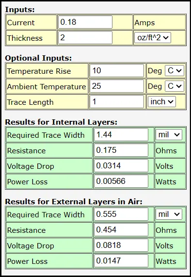
By using the above formula trace width calculated for internal layers is 1.44 mils and External layers 0.555 mils.
Via Size:
To calculate the size of a via, there are a few things to consider:
- Manufacturing cost: Opting for a larger via is going to carry lower manufacturing costs.
- Trace width: It’s generally accepted that the pad size should be somewhat larger than the via size.
- Reliability: Larger lands will be more reliable.
The IPC-2222 standard specifies minimum hole diameters for plated through-hole vias for different classes of vias:
- Minimum hole size = Maximum lead diameter + 0.25 mm (Level A)
- Minimum hole size = Maximum lead diameter + 0.20 mm (Level B)
- Minimum hole size = Maximum lead diameter + 0.15 mm (Level C)
The minimum via pad diameter can be calculated using the following equation:
L = a + 2b + c
Where:
a = Diameter of the finished hole (external layers) or diameter of the drill hole (internal layers)
b = Minimum annular ring size
c = Minimum standard fabrication allowance for interconnect lands.
Trace Length:
The maximum PCB trace length you can place between two components depends on multiple factors. These include:
- Signalling protocol: Signalling standards specify a minimum level of performance to which an interconnect should be designed. These requirements don’t guarantee the design will work, but they do give you a baseline to use for design goals.
- Component specifications: Some components can beat the requirements in your signalling standard, but this still doesn’t guarantee the channel will work.
- PCB laminate and losses: All losses in the PCB laminate will reduce the signal amplitude and produce distortion, so these loss sources need to be included when determining trace length.
- Skew and phase distortion: Skew can accumulate in some cases, depending on the routing path, due to the fiber weave effect. This is mostly problematic in the portion of the signal occupying ~20 GHz and higher frequencies, which produces phase distortion in the signal.
4. 5. What all you do to avoid heating of component in a 4-layer PCB.
Answer:
To avoid heating of components in a 4-layer PCB, you can follow these techniques:
· Thermal Via Arrays: You can turn a PCB into an onboard heat sink by incorporating thermal via arrays over copper-filled areas1. In 4-layer PCB designs, ensuring adequate thermal vias and heat dissipation paths is crucial. Placing thermal vias under power components or near heat-generating components helps conduct heat away from critical areas, reducing the risk of overheating.
· Consider Materials and Components: Before laying out your components, it’s essential to consider your board construction and material, as it plays a large role in distributing heat.
· Use Plane Partitions and Several Vias: You can use plane partitions and several vias to facilitate heat dissipation while meeting power needs in 4-layer PCBs experiencing heating problems.
· Heat Sinks: A PCB is basically a heat-generating factory because of all the heat-producing components it contains. The PCB needs some way to dissipate all that thermal energy. Generally, the answer involves heat sinks.
· Fans: Fans can also be used to dissipate heat.
· Increasing Plate Thickness and Width: This can help in heat dissipation.
· Applying Laminates: Laminates can help in reducing heat.
· Maintaining Adequate Spacing: Adequate spacing between components can help in heat dissipation.
· Integrating Heat Pipes Correctly: Heat pipes can be used to transfer heat from one part of the PCB to another.
4. 4. Advantage of multilayer PCB?
Answer:
Multilayer PCB boards offer a plethora of advantages that have contributed to their widespread adoption in various industries. Some of the key advantages include:
1. Increased Density and Miniaturization
One of the most notable benefits of multilayer PCB boards is their ability to accommodate more components within a smaller footprint. By stacking multiple layers of circuits, these boards enable increased density and miniaturization of electronic devices, making them ideal for applications where space is limited.
2. Enhanced Signal Integrity
With the continuous advancements in high-speed electronics, signal integrity becomes a critical concern. Multilayer PCB boards feature dedicated internal ground and power planes, reducing electromagnetic interference and ensuring reliable signal transmission even in complex designs.
3. Improved Power Distribution
Power and ground planes in multilayer PCB boards facilitate efficient power distribution throughout the circuit. This minimizes voltage drops and ensures a stable and consistent power supply to all components, enhancing overall device performance.
4. Enhanced Reliability
The additional layers in multilayer PCB boards provide redundancy, reducing the risk of failure due to broken traces. This increased reliability is particularly crucial in safety-critical applications and industries.
5. Design Flexibility
Multilayer PCB boards offer unparalleled design flexibility. Designers can optimize signal paths, control impedance, and implement more intricate circuitry, improving the final product’s performance and functionality.
6. Thermal Management
Heat dissipation is a significant concern in electronic devices. Multilayer PCB boards allow for integrating thermal vias and conductive planes, effectively dissipating heat and preventing overheating issues.