Project 2
Interleaving DC-DC Converter ( Interleaved Forward Converter)
Introduction:
DC-DC Converter are the converter which convert fixed DC to variable DC. There are two types of DC-DC Converter namely as non-isolated & isolated DC-DC Converter. Isolated converters are those converter which isolate both sides of voltage i.e. Higher side & Lower Side. Flyback converter,forward converter,push-pull converter etc. are the examples of isolated converter.If we want to obtain lowest voltage at its output side from high input side without disconnecting both sides then Forward DC-DC Converter is used because in forward converter the output voltage is less than input voltage. That means isolated Buck Converter is called as Forward Converter.
Why Forward Converter is used instead of conventional Buck converter ?
In case of conventional Buck Converter, to get a very low output voltage,duty 'D' needs to be very low which means the switch will be OFF for long time & thus it reduces the efficiency of converter as the input stage connects the output whenever the switch is ON. So,for very lower output voltages with good efficiency we go for isolated operation where the output voltage will be a function of turns ratio.
What is Interleaved DC-DC Converter?
Interleaving is also called as multiphasing. This is one of the technique which is used to reduce the size of filter components like inductor & capacitor. In this technique a set of parallel combination of switches, diodes & inductors are connected in parallel to common filter capacitor & load so that the current stress on individual components gets divided into number of parallel components.Thus, we can reduce the current & power stress on each component like switch, diode, inductor, etc. & increasing the the efficiency of converter. Two or more sets of converters can be interleaved. The phase shift between switch closing is 360/n, where 'n' is the number of parallel configuration.
Interleaving csn be done with other convereter as well. Under some special operating condition,nearly zero output ripple can be achieved but this happens with 50% duty in open loop configuration because in closed loop configuration, the controller automatically adjust the duty cycle to compensate for the function of input & load etc. The switches are operated 180 degree out of phase producing inductor currents that are 180 degree out of phase.
Objective of Interleaved Forward Converter:
Here we want to design a simulink model of Interleaved Forward Converter in which input voltage is 45-60 volt, output voltage 3 volt & output current 100 Ampere with above 85% of converter efficiency. Figure 1 shows the simulink model of interleaved Forward Converter in simulink software package.
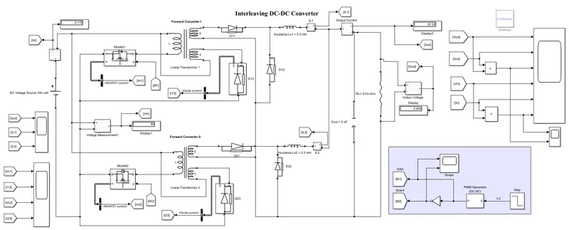
Figure 1. Simulink model of Interleaved DC-DC Converter
Before running the above model, we want to find the values of duty cycle D, switching frequency F, inductance Lx1 & Lx2, capacitance Cout, load resistance R,input & output power,etc. theorotically & then analysed graphically weather the designd model should be applicable or not.
1)Duty Cycle (D):
It is the ratio of turn ON time to the total time of switch. It is denoted by D and it is unitless quantity. In our model, we have designed such a gate drive circuit which produces two gate pulses which are 180 degree out of phase for both switches i.e MOSFET 1 & MOSFET 2. Figure 2 shows the gate drive circuit for two inverted gate pulses & figure 3 shows the inverted gate pulses of two switches.
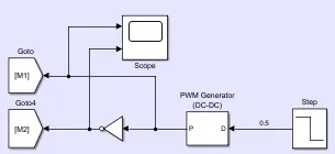
Figure 2. Gate Drive Ciruit for inverted PWM
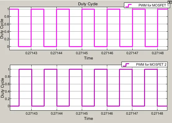
Figure 3. Inverted Gate pulses for two Switches (180 degree out of Phase)
From figure 2, we can say that the step input given to the PWM Generator block which produces a 50 % switch is to be turned ON as shown in figure 3. The PWM Generator block produces two gate pulses one is directly given to switch 1 i.e. MOSFET 1 & another is given to switch 2 i.e. MOSFET 2 via NOT gate logic block. The main function of NOT gate logic block is that it produces an inverted gate pulse that of first gate pulse.Two gate pulses are 180 degree out of phase & this is shown in above figure 3. That means when the first switch M1 is ON, the switch M2 must be OFF & vice versa.
For Forwad Converter,
To obtain zero output ripple, we assumed that the duty cycle should be 50% i.e. D = 0.5 & it is shown in above figure 3. 50 % switch is to be Turned ON & 50% switch is to be turned OFF.
Duty cycle (D) = 0.5
2) Switching Frequency (F):
The number of switch turn ON & turn OFF over a period of time is called switching frequency. Switching frequency is very important factor in power electronics, because all the operation performed by the converters depends on switching frequency. To obtain high efficiency, we assumed that switching frequncy should be higher i.e. 100 kilo-Hertz as shown in figure 4.
Switching Frequency F = 100 kilo-Hertz
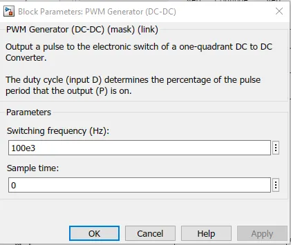
Figure 4. PWM Generator Block
3) Design of Linear Transformer:
Number of Transformer windings:
For Forward Converter,
Output Voltage = Input Voltage * Duty Cycle * (Numer of turns of secondary winding /Number of turns of primary turns)
Vout = Vin * D* (N2/N1) -----------------------------------------------------------------Formula
Let we take input voltage Vin = 60 volt; Output voltage Vout = 3 volt; Duty cycle D= 0.5
3 = 60*0.5*(N2/N1)
N2/N1= 1:10
To obtain 3 volt at its output side with 50 % duty cycle, we assumed that the voltage developed across secondary winding should be 6 volt for this, the voltage developed across primary winding would be 60 volt. We know the transformer EMF equation as
EMF = 4.44 * Frequency *Main Flux *Number of turns------------------------------EMF Equation of transformer
From above equation, we can say that the emf induced in a winding depends upon the number of turns, therefore
EMF1/EMF2 = N1/N2 = 60/6 = 10/1
To maintain the turns ratio kept constant, we assumed that the turns ratio = 10/1 = 60/6.
Let Tirtiary winding number of turns should be taken as 60.
i.e. Number of turns of primary winding N1 = 60 turns & Number of turns of secondary winding N2 = 6 turns
Turns Ratio i.e. N1/N2 = 10:1 = 60/6
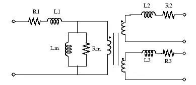
Figure 5. Linear transformer with three windings
Linear transformer is a device which transform the energy from source to load. The leakage inductance & resistance of all windings are linear i.e. and thus is called as linear transformer. It has three windings-Primary, Secondary & tertiary windings. The primary & secondary winding transfer the energy from source to load when switch is closed.Tirtiary winding is used to provide a path for magnetizing current when switch is open & to reduce magnetizing current to zero before the start of each switching period.
For Both linear transformer, the turns ratio, voltage across each winding, leackage inductance, resistance must be same as shown in following figure 6.
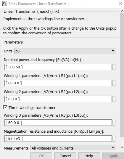
Figure 5. Winding Parameters of linear transformer
For DC Input & Output,
Output Power Pout = Output voltage * Output current = 3*100 = 300 watt
Output Power (Pout) = 300 watt
All the parameters are set to per unit system. Set the output power equal to 300 watt with fundamental frequency 50 Hz.
V1 = 60 volt ; V2 = 6 volt ; V3 = 60 volt
R1 = R2 = R3 = L1 = L2 = L3 = 0
Transformer is modelled as three ideal winding with magnetizing inductance Lm, which is placed across primary winding,leackage inductance & losses are not included in this simplified transformer model.
4) Dsign of Converter Inductance Lx:
Inductor plays an important role in this converter as it filter out the ripples present in linear transformer output. Let inductor current ripple should be leass than 5%.
Therefore, ∂ILx = 0.05
Now Inductance of Forward converter is same as Buck Converter. Hence,
Lx = Vo *(1-D) /( ∂ILx *F) -----------------------------------------------------------------Formula
Lx = 3*(1-0.5) / (0.05 * 100 *10^3)
Lx = 0.3 milli-Henry
Here Inductance of both Inductors are same and its is equal to
Lx = Lx1 = Lx2 = 0.3 mH
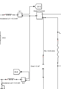
Figure 6. Two inductors fed current to Capacitor & Load
The current entering the capacitor & load resistance is the sum of inductor currents which has small peak to peak variation & frequency twice as large as individual inductor currents. i.e. twice the switching frequency. This result in a smaller peak to peak variation in capacitor current than would be achieved with a single Buck converter requiring less capacitance for the same output ripple voltage.
ILx1 + ILx2 = Ic + Iload
5) Design of Capacitance C:
The main role of capacitor is to maintain the voltage across load kept constant. The capacitance of the capacitor for Forward converter formula is also same for conventional Buck converter and is given by
Cout = (1-D) / (8*F*F*Lx*(∂Vo/Vo) -----------------------------Formula
Let the output voltage ripple should be less than 1%.
Therefore, (∂Vo/Vo) = 0.01
Cout = (1-0.5) /(8*100*100*10^6*0.01)
Cout = 2.08 * 10^-6 Farad = 2 micro-Farad
Cout = 2 uF
6) Design of Load Resistance (R):
Every devices has some its internal resistance and it is represented as R as shown in above figure 6.
According to Ohm's law,
Output voltage = Output current * Resistance ---------------------Formula
3 = 100 * R
R = 0.03 ohm = 30 milli-ohm
Construction & Working principle of Interleaved DC-DC Converter:
In Interleaved DC-DC Converter, input DC Voltage supply is connected across parallel combination of two Forward Converter. Each converter consists of a linear transformer with three windings namely-primary, secondary & tertiary winding, MOSFET's M1 & M2 which acts as a switches, a schottky diodes & inductor. The upper terminal of primary winding & lower terminal of tertiary winding is connected to the positive terminal of input dc voltage source. The lower terminal of primary winding is connected to the drain terminal of MOSFET and source terminal is connected to the negative terminal of DC input voltage source. The gate terminal of MOSFET is connected to the gate drive circuit as shown in above figure 2. The upper terminal of tertiary winding is connected to the cathode terminal of diode D13 & D23 and anode terminal is connected to the negative terminal of dc supply. The upper terminal of secondary winding is connected to the parallel combination of converter inductor Lx & diode (D12 & D22). Both these Forward converters are connected in parallel so that it feeds the total current to the common capacitor filter & load Resistor R as shown in simulink model figure 1.
To measure the input voltage & current as well as output voltage & current, we have connected voltage measurement block in parallel & current measurement block in series.
Powergui Block:
Powergui block is one of the most important block to simulate any simulink model contaiing simscape 'Electrical' specilized in Electrical Power system blocks.
It stores the equivalent simulink model which represents state space equation of the model. This block is not connected to any one of the block but it always place at the top of simulink model for optimal performance & always named as 'powergui'.
When we open this powergui block, we have to choose simulation type. If we want to display the result in variable step, then select 'continuous' option whereas if we want to display the result in fixed step or in discrete, then select 'discrete'. This discrete option is selected when our model is microprocessor or microcontroller based. Figure 7 shows the block diagram of Powergui.
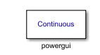
Figure 7 Block diagram of Powergui
When switch is closed,
The input dc voltage (45-60) volt in range say 60 volt is given to the primary winding of linear transformer, according to self inductance phenomenon,the emf gets induced in that winding. The voltage across primary winding is equal to input dc voltage i.e. 60 volt. The transformer basically works on the principle of mutual inductance phenomenon, the emf gets developed in secondary winding & it depends upon the number of turns. If the number of turns of secondary winding is less than primary winding, the voltage induced in secondary winding must be less than primary induced emf. To maintain the turns ratio kept constant, the voltage developed across secondary winding should be 6 volt. This 6 volt starts to flow the current through diode D12, inductor Lx1, capacitor Cout & load R.
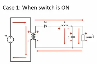
Figure 8. operation during switch closed
During this period, the magnetizing inductance of primary winding component 'Lm' gets charged & store some energy. The positive voltage will be developed across this magnetizing component Lm and is equal to input voltage i.e. 60 volt. This is not a valid. To avoid this, we place a tertiary winding across this primary winding to develope a negative voltage across Lm durinng OFF mode i.e. when switch is opened. This tertiary winding is connected across input dc voltage source via diode (D13 & D23). When the secondary winding drives the current, filter component like Inductor Lx & capacitor C stored the energy.
The voltage developed across inductor Lx = Vin - Vout ---------------------ON mode
When switch is opened,
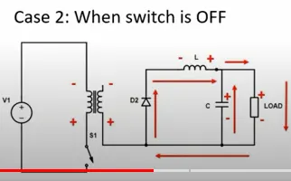
Figure 9. operation during switch opened
When switch is opened, the stored energy in inductor as well as capacitor supplies to the load to maintain the power constatnt during off mode. The inductor does not offer sudden change in current so it reverses its polarity to maintain the current in same direction, therefore we placed a diode D12 & 13 between secondary winding and inductor Lx. The capacitor gets fully charged when switch is closed & therefore it supplies the stored energy in the form of charges to the load during OFF mode od opearation.
The voltage developed across inductor Lx = - Vout ---------------------OFF mode
As the working of two forward converters are exactly same but they are 180 degree out of phase to reduce the output ripple current. The sum of inductor currents ILx1 & ILx2 is fed to the capacitor charging current & load current as shown in figure 1.
Simulation Result:
When we run above simulink model, we obtained following waveforms like output voltage & current, input voltage & current, input & output power waveform, mosfet & diode current waveform, inductor currents ILx1 & ILx2 waveform etc.
Input-Output voltage, current & Power waveform:
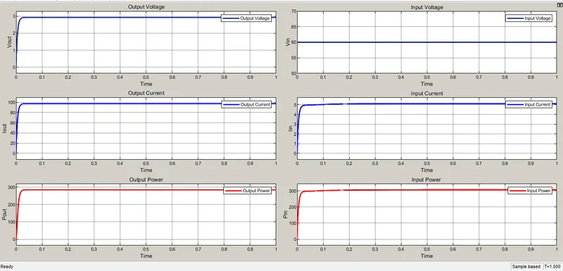
Figure 10. Input & Output Voltage, Current & Power Waveform (Zoomed Out)
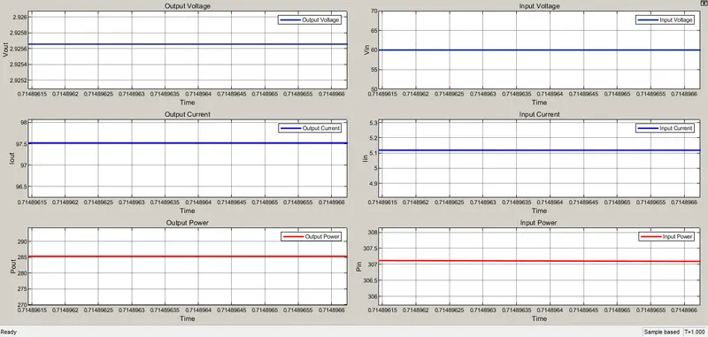
Figure 11. Input & Output Voltage, Current & Power Waveform (Zoomed In)
From above figure 10 & 11 we observed that the input voltage is 60 volt & input current is 5 Ampere. Thus the total input power equal to 300 watt. But due to some internal resistance of devices or supply system, the input power is nearly equal to 307 watt practically. The output voltage is nearby equal to 3 volt i.e. 2.93 volt, output current is 97.5 ampere which is approximately equal to 100 ampere & output power is 285 watt. The input as well as output waveforms are in pure dc.
Figure 12. MOSFET Current & Diode current waveform (Zoom Out)
Figure 13. MOSFET Current & Diode current waveform (Zoom In)
From above figure 12 & 13, we can say that when MOSFET 1 is ON simultaneously MOSFET 2 is OFF i.e. they are 180 degree out of phase. When these switches are closed, the magnetizing inductance Lm of primary windings store some energy which developes negative voltage across input dc source & it is not valid. To avoid this, the diode D13 & D23 conducts & demagnetized the magnetizing component Lm through tertiary winding when switches are opened as shown in above figure. These diodes D13 & D23 demagnetize Lm before next gate pulse applied to the switch.
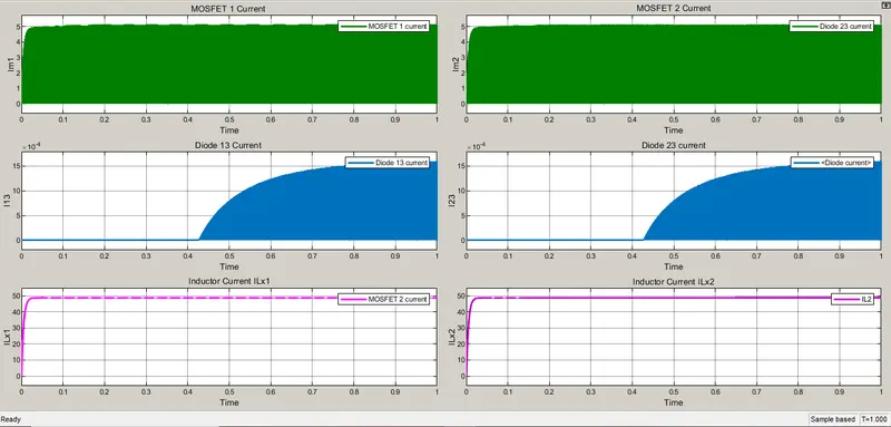
Figure 14. Respective MOSFET current, diode current & Inductor current waveform (Zoom Out)
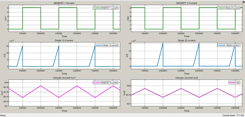
Figure 15. Respective MOSFET current, diode current & Inductor current waveform (Zoom In)
From figure 12 & 14, we clearly observed that during time period from 0 to 0.45 sec, the switches perform their operation (ON-OFF) simultaneously and diodes D13 & D23 does not conduct because during this interval the magnetizing component Lm stored the energy. After time 0.45 sec, the diodes starts to conduct through tirtiary winding. Figure 15 shows the respective MOSFET current, diode current & inductor current waveform of typical forward converter. Here we observed that when the switch is ON, inductors Lx1 & Lx2 start to charge upto peak value and when switch is OFF, these inductors start to discharge & simultaneously diodes D13 & D23 conducts for a short period of time before next switching operation is performed. Here both inductors supply equal current to the capacitor as well as load. The peak value of individual current is 50 ampere.
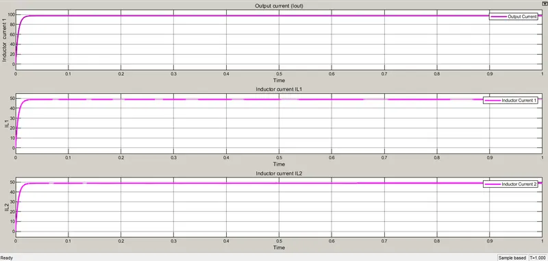
Figure 16. Inductor currents waveform (Zoom Out)
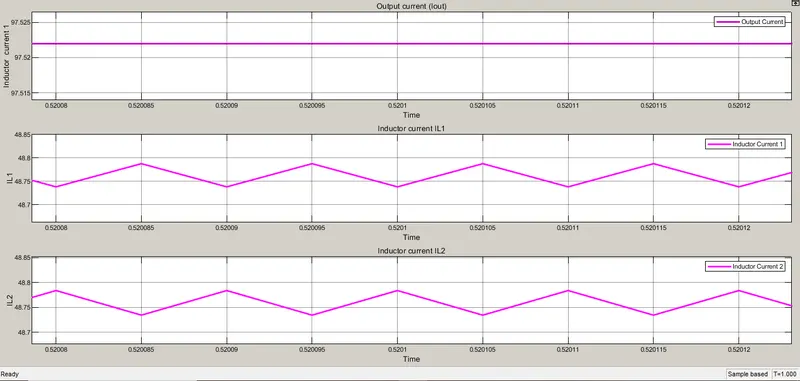
Figure 17. Inductor currents waveform (Zoom In)