Project 1
Project 1
Simulation & Design of Power Converter for EV using Matlab/Simulink
Introduction:
The demand for the control of electric power for electric motor drive systems & industrial controls existed for many years.In the recent past, the power electronics has revolutionalized the concept of power conversion & for the control of electric motor drives. The word Power Electronics combines three terms namely as Power, Electronics & Control. Power deals with static & rotating power equipement for the generation, transmission & distribution of electric energy. Electronics deals with solid state devices & circuits for signal processing to meet the desired control objectives. Control deals with the steady state & dynamic characteristics of closed loop system. In short Power electronics is defined as the applications of solid state electronics for the conversion & control of electric power. Power electronics are based primarily on the switching of power semiconductor devices. Power handling capacity & switching speed of power devices are the two most important criterions related to power devices. The microprocessors & microcontrollers are being used for control & synthesizing the control of the power semiconductor devices. That means power semiconductors acts as a muscles & microprocessors acts as a brain for modern power electronic equipment.
General requirements of Power Devices:
- They should be capable of handling large current & power.
- They should withstand a very high voltage in OFF State condition.
- They should be capable to operate as a switch at a very high frequency.
- They should have low on state voltage, on state resistance & a very high off state resistance.
Application areas of Power Electronics:
- Electric vehicles
- Heat control (Induction Heating)
- Vehicle Propulsion system
- Conveyors, cranes & hoists control
- DC & AC motor control
- High Voltage Direct Current (HVDC) system
- Washing machines, blowers, drayers,furnaces & refrigeratos
- VAR (Reactive Power) Compensation, etc.
Power semiconductor devices are broadly classified into three categories as follows:
1) Rectifire : which convert AC to DC supply.
2) Inverter: which convert DC to AC supply.
3) Chopper (DC-DC Converter): which convert fixed DC to Variable DC supply.
Chopper (DC-DC Converter)
Introduction:
In many industrial applications,it is required to convert a fixed-voltage DC source into variable-voltage DC source. A dc converter converts directly from dc to dc & is simply known as a DC converter. A dc converter can be considered as dc eqiuvalent to ac transformer with continuously variable turns ratio. Like a transformer, it can be used to step up or step down a dc voltage source.DC converters are widely used for traction motor control in electric automobiles. They provide a smooth acceleration control, high efficiency & fast dynamic response. DC converters can be used in regenerative braking of DC motors to return energy back into the system & this feature results in energy saving for transportation systems with frequent stops.
A fixed voltage of dc source can be converted to a variable dc voltage on a load by placing a high speed switch between the dc source & the load. This high speed static switch is called as 'chopper'.A chopper is a thyristor based ON/OFF switch that connects load to and disconnect from the supply & produces a chopped load voltage from a constant input supply voltage.
The average output voltage V0 can be changed in three ways:
1) By varying ON time, (Ton),
2) By keeping ON time or OFF time constant & varying the frequency
3) By varying both Ton & frequency
The output voltage V0 can be controlled by periodic opening & closing of the switch. There are two schemes by which the duty cycle can be varied leading to the variation in output voltage. These method are,
1) Constant Frequency System ( Pulse Width Modulation)/(PWM Technique)
2) Variable Frequency System ( Frequency Modulation Technique)
In constant frequency system, only the ON time is varied by keeping the chopping period T constant. Variation of Ton means adjestment of pulse width. whereas in variable frequency system, the chopping frequency is varied either Ton or Toff constant. Constant frequency system is better than the variable frequency system because variation in frequency gives lots of drawbacks like it requires a difficult filter design, more possibility of interference with signaling & telephones line signals, etc. Therefore, constant frequency system is widely used & this system is also called as 'Pulse Width Modulation'. In PWM, low range of duty cycle is not possible.
Classification of Chopper ( DC converter):
DC-DC converter can be classifed as non-isolated & isolated converter. Non-isolated converter are those which directly convert from dc to dc supply but Isolated converter are those which convert first from dc to ac & then ac to dc. That means non-isolated converter operate in single stage while isolated converter operate in two stages. Isolated converter require three major components as Inverter, Transformer & Rectifier.
Choppers are classified on various basis. According to output voltage level compared with input voltage level, choppers are broadly classified as :
1) Step-down chopper ( Buck converter)
2) Step-Up chopper ( Boost converter)
In step-down chopper, the chopping element is connected in series with load & source. So it is also called as series chopper or Buck converter. For step up chopper, the chopping element is connected in parallel with load & source therefore it is called as parallel chopper or Boost converter. The basic circuit diagram of step-down & step-up chopper is shown in figure 1.These are the non isolated converter.
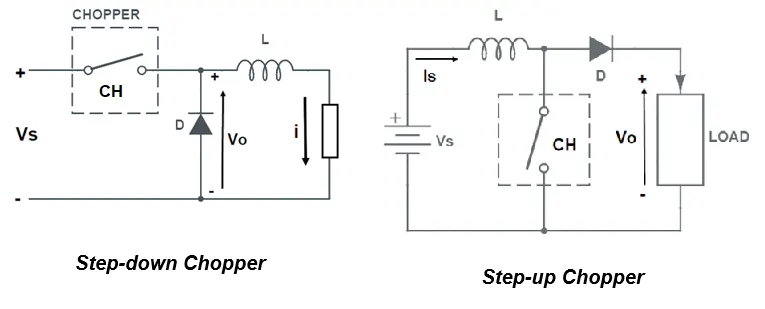
Figure 1. Basic circuit diagram of step down & step up chopper
*******************************************************************************************************************
Project Number : 1
Buck Converter in CCM
Input Voltage : 40-50 volt ; Output Voltage: 30 volt ; Power level: 500 watt
Objective of Step-down converter (Buck Converter):
Our main objective is to design a dc-dc converter such that the conveter should convert 40 to 50 Volt from the battery pack to the the 30 Volt loads with power level 500 watt. For this purpose, we want to use the step down chopper. With the help of this chopper, we can easily convert high input dc voltage to the low dc output voltage.The circuit diagram of buck converter is shwon in figure 2 with LC filter & Resistance R as a load.
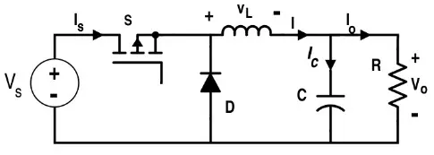
Figure 2. Circuit diagram of Buck converter
In above diagram,
Vs= Supply dc voltage in volts;
Is= Supply dc current in ampere;
S= High speed switch like MOSFET;
D= Freewheeling diode;
L= Inductor in henry;
VL= Lotage across inductor;
I= Indutor current in ampere;
R= Load Resistance in ohm;
V0=Average output voltage in volt;
C= Capacitor in Farad;
Ic= current through capacitor in ampere.
What is CCM?
CCM stands for Continuous Conduction Mode. The converter is said to be operating in continuous conduction mode if the load current never becomes zero during the complete cycle.To operate the converter in CCM, the value of inductance is chossen to be high so that it doesn't discharge emmediately during switching OFF position.
Condition for CCM, L > 1.05 Lcrit
Inductor current (IL) = Positive
Minimum value of Inductor current (ILmin) = Not eqaul to zero.
where, L(crit) is nothing but the critical value of inductance at which minimum value of inductor current riches to zero.
Now, we will start to design a simulink model of Buck converter in CCM with the help of simulink software package as shown in following figure 3.
Simulink Model of Buck Converter in CCM:
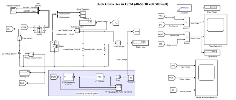
Figure 3. Simulink model of Buck Converter in Continuous Conduction Mode
Figure 3 shows the simulink model of BUCK Converter which is operated in Continuous Conduction Mode (CCM). Before developing the simulink model, we want to know the design parameters like Inductance L, Capacitance C, Load Resistance R, duty cycle K,switching frequency f and all the block parameters which are required at the time of designing.First we will analyse in detail & then after we will be able to design a particular BUCK converter in CCM. We know the values of input voltage Vi=40-50 volt, output voltage V0=30 volt & load needs an output power P=500 watt. Our requirement is that the output voltage will be 30 volt which is constant with output power of 500 watt.
Bolck Parameters
Now, we will explain all the block parameters individually which we will have been taken at the time of designing of Buck Converter. What is the function of particular block, why we choose?, what are the block parameters ?All the necessary requirements we will explain in detail step by step as follows.
DC input Source:
The input supply to the Buck converter is in the form of DC (Direct Current) which is equal to 40 to 50 volt in range. With help of voltage measurement & current measurement block, we can easily measure & display the input Voltage (Vi) & input current (Ii) as well. The dc source block & its waveform is shown in following figure 4.
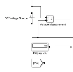
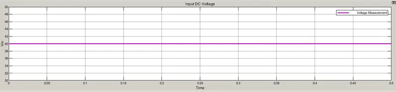
Figure 4. DC input Source & input voltage waveform for BUCK converter in CCM
************************************************************************************************************************************
Switch Designing for Buck Converer:
Switch designing is one of the most important factor in design domain. Because all the operation performed by any converter depends upon their switching pattern. So, here we are using MOSFET as a switch for connecting & disconnecting the input as well as output side while the freewheeling didoe acts as a forward path during discharging of an inductor i.e. during OFF time.
i) MOSFET:
MOSFET stands for Metal Oxide Semiconductor Field Effect Transistor. We have taken Metal Oxide Semicondutor Field Effect Transistor MOSFET) as a switching device. For high power applications, this is most preferable & it has better response as compared to other switching device. For low switching applications, this MOSFET is suitable. MOSFET has three terminals - Drain (D), Source (S) & Gate (S). Drain is connected to the input side, Source is connected to the output & Gate terminal is connected to the Gate Drive Circuit (PWM Generator).
When switch is ON, the input is connected to the output side & during this Turn ON interval, the inductor L gets start to charge. As, the output is connected to the input side thus increasing the efficiency of converter. Therefore if the converter operated as a BUCK converter, the turn ON time must be higher than turn OFF time.
Ton > Toff
There are two types of MOSFET- N-Channel & P-Channel. But P-channel MOSFET is expensive, less current rating & it also require complicated gate drive circuitry. There are some advantage of N-Chanel MOSFET as follows:
* Less Expensive
* Less Voltage Drop across MOSFET as compared to BJT
* It requires simple gate drive circuit.
* High current rating etc.
The voltage drop across MOSFET is very low & therefore we prefer this device as a switch for increasing the efficiency.Theorotically, MOSFET Voltage & current rating as
MOSFET Voltage rating:
Maximum switch voltage = input voltage
Vmosfet = Vin = 40-50 volt say 40 volt
MOSFET current rating:
Maximum switch current = Input current = Maximum output current * Duty cycle
Imosfet = 17.08 * 0.6 = 10.2 approximately equal to 10 ampere.
The block diagram, MOSFET Voltage & MOSFET current waveform are shown in following figure 5.
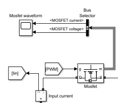
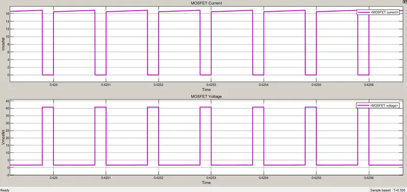
Figure 5. Block dioagram of MOSFET, MOSFET current & MOSFET Voltage waveform
From figure 5, we observed that during the switch is ON, current flowing through the MOSFET is near about 16.23 ampere & voltage across it is zero. Wheresa during the switch is OFF, the current flowing through it is zero but the voltage across MOSFET is 40 volt.
ii) Schottky Diode:
Schottky diode is also acts as a switching device but it is uncontrolled in nature & it freewheels the load current during turn OFF time. Schottky diodes are used because the voltage drop across the Schottky diode under forward bias is lower than the voltage drop across an ordinary silicon diode, once again, improving efficiency.Theorotically,
Diode Voltage:
RMS value of Diode voltage = - Input Voltage
Vdiode = - (40-50) volt say -40 volt
Diode Current:
Forward diode current = Maximum output current * ( 1- duty cycle)
Idiode = 17.08 * 0.4 = 6.8 approximately equal to 7 ampere
The block diagram, Diode voltage & current waveform as shown in following figure 6.
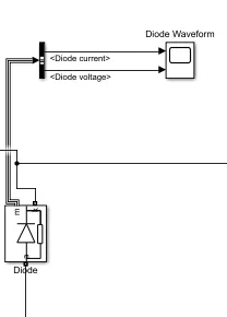
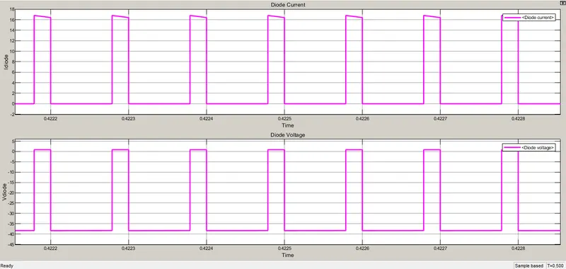
Figure 6. Block dioagram of Diode, Diode current & Diode Voltage waveform
From above figure 6, we observed that when the diode conducts, the voltage across it is zero while when the diode is in reverse bias, the voltage across diode is -40 volt. Negative voltage will appear across diode during Switch Turn ON because the diode is in reverse bias.
That means,
During Turn ON time : MOSFET - ON & Schottky Diode - OFF.
During Turn OFF time : MOSFET - OFF & Schottky Diode - ON.
*****************************************************************************************************************
Design parameter of duty cycle D & switching frequency f:
i) Duty cycle: It is the ratio of ON time of switch to the total time period of switch. It is denoted by 'D'. It is unitless quantity because it is the ratio of two same quantity. mathematically, it is given by,
Duty cycle = ON Time /(Total Time);
but Total time= ON Time+ OFF Time;
Therefore, Duty cycle= ON Time/(ON Time + OFF Time)
For Buck Converter,
Output Voltage = Duty Cycle * Input Voltage
Duty cycle = Output voltage / Input voltage -------------------------------------------------------------------------------------------------------Formula
D = Vo/Vin = 30/50 = 0.6 to 30/40 = 0.75
Duty cycle D = 0.6 to 0.75
That means, 60 to 75 % the switch is turned ON. This is shown in following PWM waveform figure 7.

Figure 7. Duty cycle (PWM) waveform of switch
ii) switching frequency f: Number of cycles performed in one second is called frequency. Switching frequency means number of ON/OFF switching operation performed in time T second. It is denoted by 'f' & it is measured in Hertz (Hz). We have not known the value of switching frequency, So we want to assume as per our requirement.
We assume that, the switching frequency should be 10kHz.
Switching Frequency (f) = 10 kHz = 10,000 Hz
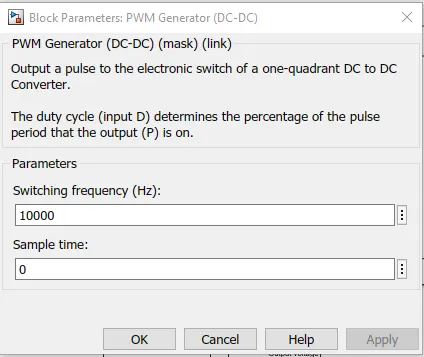
Figure 8. PWM Generator block parameter showing switching frequency
Higher value of switching frequency reduces the size of inductor as well as capacitor because switching frequency is inversly proportional to inductance L & capacitance C & thus reduces the cost as well but it increases the output ripples.
*******************************************************************************************************************************
Design of Load Resistance (R):
There are some loads which require less output voltage to run. Therefore we assumed that the load is represented as a resistance R. The total load resistance is given by
Power = (output voltage)^2 / Load Resistance
P=Vout^2/R ----------------------------------------------------------------Formula
R = Vout^2/P
R= (30*30) / 500 = 1.8
Load Resistance R = 1.8 ohm
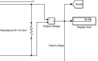

Figure 9. Block diagram of Resistance acts as a load & voltage across load waveform
***********************************************************************************************************************
Design Parameter of Inductor current, Inductor current ripple (∂IL) & Peak current rating of Inductor:
Before designing the inductor, it is necessary to know the values of inductor current IL, inductor current ripple ∂IL & peak current rating of inductor ILmax. So, first we will calculate these values then it will be easy for finding out the value of inductance L.
In Buck converter, the inductor is connected to the load side therefore inductor current equal to load current & is given by
IL = Iout = Output voltage / Load resistance = Vout/R ------------------------------------------------------------------------------Formula
IL = Iout = 30/1.8 = 16.67 amp
Inductor current = Output current Iout = 16.67 Ampere
Inductor Ripple current: Ripple current is the change in current from time 0 to Ton or from Ton to the end of switching cycle. The ripple current is very important because it is needed to size of inductance value of the inductor.
Let us assume that,
Inductor current ripple ∂IL = 5% = 0.05 * IL;
Now we want to design a switching inductor such that the current is continuous & the inductor current ripple is less than 5 % of the average output current.
Therefore, Inductor ripple current (δI) = 5% * Maximum output current
δI = 0.05 * Iout = 0.05 * 16.67 = 0.834 Ampere
Inductor current ripple (∂IL) = 0.834 Ampere
Peak current rating of Inductor: ILmax & ILmin
Peak current rating of inductor can be found using maximum value of inductive current.
ILmax = IL + (∂IL/2) & ILmin = IL - (∂IL/2) ---------------------------------------------------------------------------Formula
ILmax = 16.67 + (0.834/2) = 17.087 & ILmin = 16.67 - (0.834/2) = 16.253
ILmax = 17.087 Ampere & ILmin = 16.253 Ampere

Figure 10. Waveform of Inductor current
From above figure 10, we can say that the value of inductor current is 16.6 ampere with current ripple of 0.45 something. Peak value of current is also equal to 16.9 & 16.45 ampere.
***************************************************************************************************************************
Design of Inductance (L):
Inductor is a enegy storage device which store energy during On time & feed the stored energy to the load during OFF time to maintain the operation in continuous mode.Now we want to design a switching inductor such that the current is continuous & the inductor current ripple is less than 5 % of the average inductor current.Before designing the correct inductor value, it is necessary to know the ripple current & we have calculated the value of inductor current ripple above.
For a Buck Converter,
Lcrit = Rmax * (1-Dmax) / ( 2*f ) ---------------------------------------------------------------------------Formula
Substitute the values of R, D & f we get the value of inductance L,
Lcrit = 1.8 * (1-0.6)/ (2* 10*10^3) =1.438
Lcrit =1.438 milli-Henry
To make the operation in continuous conduction mode, hence the value of L should be greater than 1.05 * Lcrit (minimum value of L) & the value of inductance L is assumed to be in terms of integer value for the sake of simplicity at the time of design of inductor.
L > 1.05 * Lcrit ------------------------------------------------Condition for CCM
L > 1.05 * 1.438 = 1.5099
Therefore, we assumed that, the value of Inductance L should be higher & it is taken as 1.6 milli-Henry.
Inductance of Inductor L = 1.6 mH
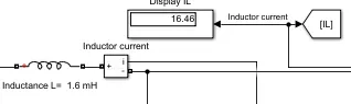
Figure 11. Symbolic representation of Inductor L
Why we select higher value of inductance L ?
> To make the operation in Continuous Conduction Mode (CCM)
> To reduce the output ripple.
Small inductor will give higher ripple & big inductor will result to lower ripple current.
*********************************************************************************************************************
Design of Capacitance (C):
The role of capacitor in Buck converter is to help ahieve a good output regulation.It is critical to select the right capacitance value. During ON time, the output capacitor gets charged. In this time, the current Ic is enterd to the capacitor. On the other hand, during OFF time, the output capacitor gets discharged. In this time, the current is leaving from the capacitor & it helps to provide the demand of load R.
Peak to peak capacitor voltage is given by,
δVc=δVo = δI /( 8*f*C) ------------------------------- Formula in terms of inductor ripple current 'δI'
δVc=δVo = (Vi * D* (1-D) /( 8*f^2*L*C) ------------Formula in terms of Input voltage 'Vin'
δVc=δVo = (Vo* (1-D)) /( 8*f^2*L*C) ----------------Formula in terms of Output voltage 'Vo'
Let us assume that
Output voltage ripple ∂Vo/Vo = 1% = 0.01;
We have to design the output capacitor such that the output voltage ripple is less than 1%. i.e.
δVo/Vo = 0.01
Therefore, minimum value of output capacitance Cout is given by,
Cout = (1-D)/ (8*f^2*L*(δVo/Vo)) ---------------------------------------Formula
Cout = (1-0.6) /( 8*10*10*10^6*1.6*10^-3*0.01) = 31.25 micro-Farad
Minimum value of Capacitance Cout = 31.25 uF
During OFF time, the capacitor helps to prevent the regulation from falling too much. Therefore, the capacitance must be large enough to maintain the desired regulation or ripple voltage. If the capacitance is too low, the output voltage will lag too much therefore output regulation is bad. To avoid this problem, we assumed tht the capacitance value should be higher than calculated value.
Take, capacitance of the capacitor is given by,
Capacitance Cout = 35 micro-Farad
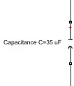
Figure 12. Symbolic representation of Capacitance C
As the capacitor is connected in parallel with load resistance R, thus the voltage across capacitor is same as that of load voltage & it is equal to 30 volt.
********************************************************************************************************************************
Input & Output Power
Power :
The product of voltage & current gives the power. Mathematically,
Input Power is given by
Input power (Pin) = Input voltage (Vin) * Input current (Iin)
Pin = 40 * 16.67 = 666.67 = 667 watt
Input Power Pin = 667 watt
Output power is given by
Output Power (Pout) = Output Voltage (Vout) * Output current (Iout)
Pout = 30 * 16.67 = 500.1 = 500 watt
Output Power Pout = 500 watt
Practically, the output power is always less than input power because due to some switching losses, we get less power at its output side.
Here, we can calculate the switching losses as
Switching losses = Input power (Pin) - Output Power (Pout) = 667 - 500 = 167 watt.
Figure 13 shows the block digram of power & input,output power waveform.
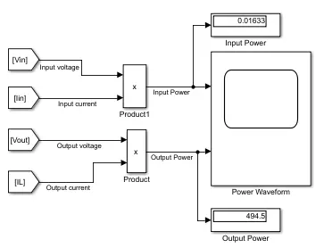
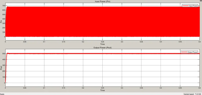
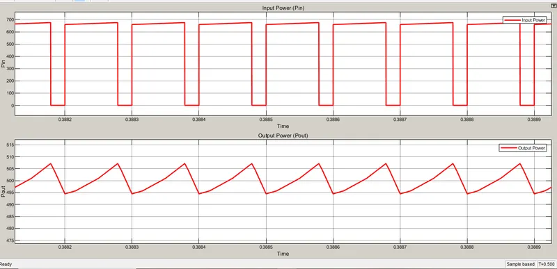
Figure 13. Input & Output Power Waveform of BUCK Converter in CCM ( Zoom out & Zoom In)
*************************************************************************************************
Powergui Block
Powergui block is one of the most important block to simulate any simulink model contaiing simscape 'Electrical' specilized in Electrical Power system blocks.
It stores the equivalent simulink model which represents state space equation of the model. This block is not connected to any one of the block but it always place at the top of simulink model for optimal performance & always named as 'powergui'.
When we open this powergui block, we have to choose simulation type. If we want to display the result in variable step, then select 'continuous' option whereas if we want to display the result in fixed step or in discrete, then select 'discrete'. This discrete option is selected when our model is microprocessor or microcontroller based. Figure 14 shows the block diagram of Powergui.
Figure 14. Block diagram of Powergui
***********************************************************************************************************************************
Closed Loop Feedback system
Practically, the output voltage must remains constant to give smooth operation of any electrical device. But due to the variation in input voltage, the output voltage also varied. To avoid the variation in output voltage, we must require to maintain it in constant level. For this reason, we design a closed loop feedback system. In which we compared the actual output voltage to the reference voltage. Here the reference voltage is 30 volt. Both reference voltage as well as actual output voltage is given to the error block ( Sum Block) as a input. This error block gives the diffence between two voltages as an output. The output of error block is given to the PI Controller. PI (Proportional,Integral) Controller is a special type of controller in control system which is widely used in industry & it creates an output which is given to the PWM ( Pulse Width MOdulation) Generator block. Then after this PWM generator genrate duty cyccle for a switch (MOSFET) so that the output voltage must remains constant during any input variation. But the input voltage variation is always greater than output voltage i.e. 30 volt because this converter acts as a BUCK in which the input voltage must be greater than output voltage. Figure 15 shows the block diagram, PI controller input, output as well as duty cycle of BUCk convereter.
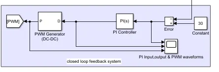
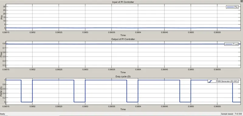
Figure 15. Closed loop feedback system for BUCk Converter in CCM
***********************************************************************************************************************
Construction & Working Principle of BUCK Converter in CCM
Figure 3 shows the simulink model of BUCK converter which is operated in Continuous Conduction Mode. BUCK Converter is a device which step down the input voltage. Here we are using MOSFET as a switching device because the voltage drop across its terminal is less as compared to other switching device & thus helps to improve efficiency. The input voltage 40-50 volt dc source is connected to the drain of MOSFET. Here MOSFET acts as a switching device. The gate terminal of MOSFET is connected to the PWM generator which produce appropriate pulses for switch under different dynamic condiction. The source terminal is connected to the combination of cathod of Schottky diode & first end of the inductor L. Measurement terminal m is connected to the bus selector for obtaining MOSFET voltage & MOSFET current waveform.
Schottky diode is a special type of diode in which a very low voltage drop occurs across its terminal hence it helps to improve efficiency. The anode terminal is connected to the negative terminal of DC input source. The measurement port E is connected to the bus selector so that it is easy to show the diode voltage & diode current waveform. From the above design data, we have selected an inductor value which is higher than critical value to give CCM mode & equal to 1.6 milli-Henry.
The second terminal of inductor is connected to the parallel RC circuit in which the value of capacitance is 35 micro-farad with 1.8 ohm load resistance. To obtain the constant output voltage with constant output power, we have designed a closed loop circuit which is already explained in detail above. Before running this model, check the powergui block. This block is not connected to any other block but it is important to present in every simulink model. Because it stores the simulink model which represents state space model. Specially this block is used where simscape specialized electrical power system blocks are used.
The BUCk converter in CCM operate in two modes of operation:
ON Mode : When switch is ON
When switch is ON, the input is connected to the output side, the voltage across switch is zero and voltage across diode is neagtive of input voltage. The turn on voltage Vin-Vout. In Buck converter, the inductor L is connected in series with input as well as output & therefore it stores some energy during this time ON interval.
OFF Mode: When switch is OFF
When switch is OFF, the output is disconnected from input side, the voltage across switch appears and is equal to input voltage. During this interval, inductor L supply their stored energy to load resistance to maintain the constant output voltage when input is cut off.This inductor current complete their path through load R & schottky diode. When inductor discharge completely, then again switch pulse is given to the MOSFET to operate in ON mode. The value of inductor is selected so that it doestn't discharge completly to maintain the operation in CCM. During this time OFF, the turn off voltage is equal to -Vout.
When we run the above simulink model, we get different waveforms like input, output voltage waveform, inductor current waveform, input, output power waveform, MOSFET voltage, current waveform, Diode voltage, current waveform, PI controller input, output waveform & PWM (pulse) waveforms we have seen above individually.
Simulation Results
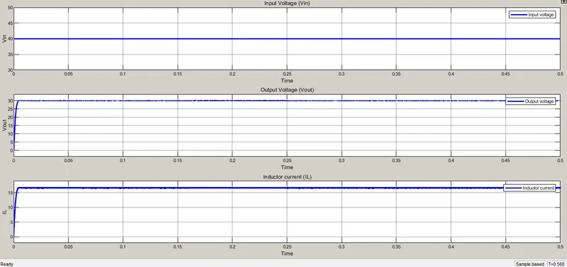
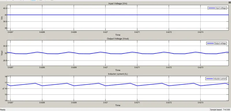
Figure 16. Input, Output Voltage & Inductor current waveform (Zoom Out & Zoom In)
From above figure 16 & 13, we observed that the input voltage is 40 volt, output voltage is 30 volt, inductor current is 16.67 ampere in CCM with output power of 500 watt.
******************************************************************************************************************************
Different Dynamic Conditions
Suppose, the input voltage is varied. So we will analyse how to affect on our output voltage as well as output power.
Let Input Voltage Vin = 45 volt;
Simulation Result:
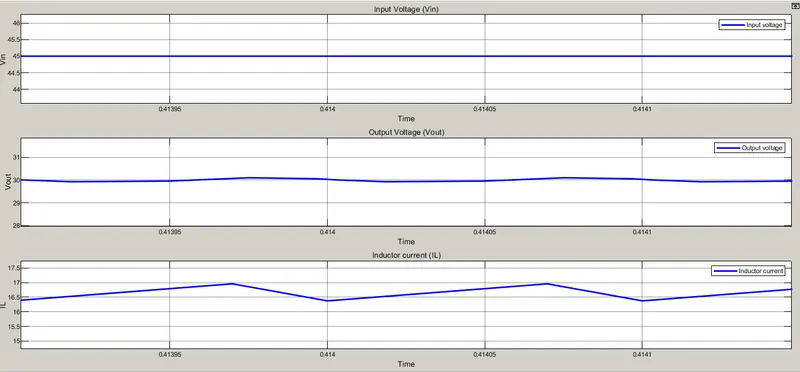
Figure 17. Input, output voltage & inductor current waveform with 45 volt input voltage supply
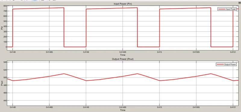
Figure 18. Input & Output Power Waveform with input voltage 45 volt dc.
Let Input Voltage Vin = 50 volt;
Simulation Result:
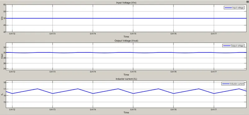
Figure 19. Input, output voltage & inductor current waveform with 50 volt input voltage supply
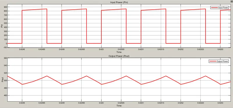
Figure 20. Input & Output Power Waveform with input voltage 50 volt dc.
From above waveforms 17,18,19 & 20, we observed that whenever the input voltage gets changed,it does not affect on output voltage as well as output power due to the presence of closed loop feedback circuit. The output voltage Vout & output power Pout ramains constant & which is equal to 30 volt with 500 watt power rating. Hence, our main objective is achieved with the help of this converter.
Comment:
> Buck Converter step down the input voltage
> Whenever the input voltage gets changed, the output voltage & output power remains constant.
> BUCK converter operated in CCM mode gives higher efficiency because, the switch is continuously connect input & output side & thus helps to improve efficiency.
**********************************************************************************************************************************************
**********************************************************************************************************************************************
Project Number : 2
Buck Converter in DCM
Input Voltage : 10-20 volt ; Output Voltage: 5 volt ; Power level: 100 watt
Introduction:
We have already discussed the basic information of BUCK Converter. Buck converter step down the input voltage level. Here we want to operate the BUCK Converter in DCM (Discontinous Conduction Mode
). The input voltage is 10 to 20 volt dc, output voltage will be 5 volt dc with power demand of 100 watt.
Before designing this BUCK converter in DCM, firstly we know
what is DCM ?
DCM Stands for Discontinous Conduction Mode. The minimum value of inductor current reaches to zero for some interval of time,is called discontinuous conduction mode.
In DCM, there will be three modes of operation,
1) ON mode of operation
2) OFF mode of operation before inductor fully discharge.
3) OFF mode of operation after inductor fully discharge.
In OFF mode of operation after inductor fully discharge, the voltage across inductor is zero.
In DCM, the duty cycle of BUCK Converter is
Vout / Vin = (D/(D+D1)) ---------------------------------------------Formula
where, D = Duty cycle during ON mode
D1 = Duty cycle during OFF before inductor fully discharge.
Simulink model of BUCK Converter in DCM
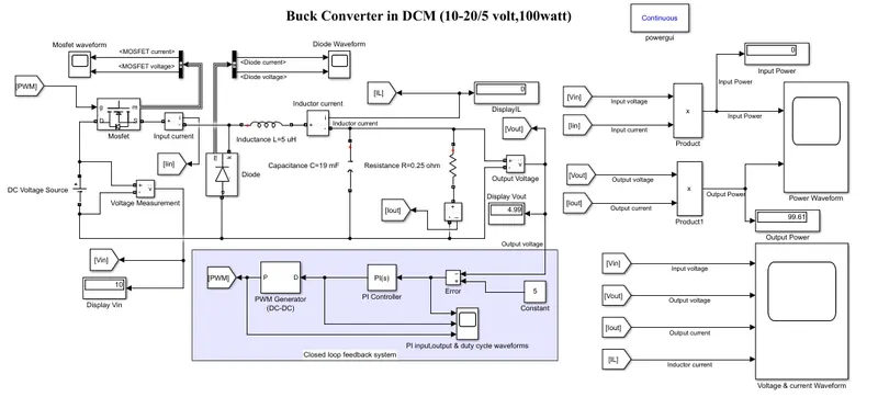
Figure 1. Simulink model of BUCk converter in DCM
Construction & Working Principle:
Figure 1 shows the simulink model of BUCK converter operated in DCM. Here the input voltage range in between 10 to 20 volt dc is provided by DC voltage source. The positive terminal of source is connected to the drain terminal of the MOSFET. Gate terminal 'g' is connected to the output of PWM generator for providing the gate signal to the switch. The source terminal 's' is connected to the firsst terminal of inductor L and cathod terminal of schottky diode. The value of inductance of the inductor is 5 micro-henry. The second terminal of inductor is connected to the parallel RC circuit whose capacitance is 19 milli-farad & load resistance is 0.25 ohm.
To obtain constant output voltage i.e. 5 volt across load resistance, we designed a closed loop feedback circuit in which actual ouput voltage compared with refence voltage. Here, the reference voltage is taken to be 5 volt. The diffence between these two voltages is given to the PI ( Proportional & Integral ) controller.Then PI controller produces a such output as PWM generator gives accurate gate pulse to the MOSFET to mantain the constant output voltage Vout as well as output power Pout.
Here, Buck converter wants to operate in DCM (Discontinuous Conduction Mode). Therefore, we have to select the value inductance L should be less than 1.05 times critical value of inductance . Before running the above simulink model, it is necessary to find out the various parameters like duty cycle D, switching frequency F, loar resistance R, inductor current IL, inductor current ripple ∂IL, peak inductor current current rating , output current Iout, input & output power etc.
Step by step we will find out the design parameters as follows:
Design parameter of duty cycle D & switching frequency f:
i) Duty Cycle :
It is the ratio of ON time of switch to the total time period of switch. It is denoted by 'D'. It is unitless quantity because it is the ratio of two same quantity. mathematically, it is given by,
Duty cycle = ON Time /(Total Time);
but Total time= ON Time+ OFF Time;
Therefore, Duty cycle= ON Time/(ON Time + OFF Time)
For Buck converter, duty cycle is given by
Output Voltage = Duty Cycle * Input Voltage
Duty cycle = Output voltage / Input voltage -------------------------------------------------------------------------------------------------------Formula
D = Vo/Vin = 5/20 = 0.25 to 5/10 = 0.5
Duty cycle D = 0.25 to 0.5
That means, 25 to 50 % the switch is turned ON. This is shown in following PWM waveform figure 2.

Figure 2. Duty cycle (PWM) waveform of switch for BUCK converter in DCM
switching frequency f: Number of cycles performed in one second is called frequency. Switching frequency means number of ON/OFF switching operation performed in time T second. It is denoted by 'f' & it is measured in Hertz (Hz). We have not known the value of switching frequency, So we want to assume as per our requirement.
We assume that, the switching frequency should be 10kHz.
Switching Frequency (f) = 10 kHz = 10,000 Hz
Figure 3. PWM Generator block parameter showing switching frequency
Higher value of switching frequency reduces the size of inductor as well as capacitor because switching frequency is inversly proportional to inductance L & capacitance C & thus reduces the cost as well but it increases the output ripples.
*******************************************************************************************************************************
Design of Load Resistance (R):
There are some loads which require less output voltage to run. Therefore we assumed that the load is represented as a resistance R. The total load resistance is given by
Power = (output voltage)^2 / Load Resistance
P=Vout^2/R ----------------------------------------------------------------Formula
R = Vout^2/P
R= (5*5) / 100 = 0.25
Load Resistance R = 0.25 ohm
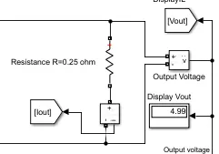

Figure 3. Block diagram of Resistance acts as a load & voltage across load waveform
*********************************************************************************************************************
Design Parameter of Inductor current, Inductor current ripple (∂IL) & Peak current rating of Inductor:
Before designing the inductor, it is necessary to know the values of inductor current IL, inductor current ripple ∂IL & peak current rating of inductor ILmax. So, first we will calculate these values then it will be easy for finding out the value of inductance L.
For Buck converter operated in DCM ,
Iout = Output voltage / Load resistance = Vout/R ------------------------------------------------------------------------------Formula
Iout = 5/0.25 = 20 amp
Output current Iout = 20 Ampere
Inductor current IL:
In case of BUCK converter operated in DCM, the inductor current is equal to input current because the inductor is connected in series with input dc source.
Therefore, inductor current can be found from duty ratio,
Input current / Output current = Duty cycle --------------------------------------------Formula
Inductor current / Output current = Duty cycle ---------------------------------------Iin = IL
IL / 20 = 0.25 ;
IL = 50 ampere
Inductor current IL = 50 Ampere
Inductor Ripple current: Ripple current is the change in current from time 0 to Ton or from Ton to the end of switching cycle. The ripple current is very important because it is needed to size of inductance value of the inductor.
Now we want to design a switching inductor such that the current is discontinuous & therefore the current ripple is too much high in DCM mode.
Therefore, Inductor ripple current (δI) = Maximum inductor current
δIL = IL = 50 Ampere
Inductor current ripple (∂IL) = 50 Ampere
Peak current rating of Inductor: ILmax & ILmin
Peak current rating of inductor can be found using maximum value of inductive current.
ILmax = IL = 50 ampere & ILmin = 0 ampere ---------------------------------------------------------------------------Condition for DCM
The minimum value of inductance ILmin must be zero for some interval of time in DCM.
ILmax = 50 Ampere & ILmin = 0 Ampere
Figure 4 shows the output current and inductor current waveform as follows.
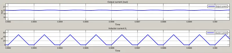
Figure 4. Output current & inductor current waveform of BUCK converter in DCM
From above figure 4, we observed that the output voltage is nearly equal to 20 ampere, inductor current IL & inductor current ripple δIL is 50 ampere, minimum & maximum value of inductor current is 0 ampere & 50 ampere respectively.
**********************************************************************************************************************
Design of Inductance (L):
Inductor is a enegy storage device which store energy during On time & feed the stored energy to the load during OFF time to maintain the operation in continuous mode but we want to design a switching inductor such that the current is discontinuous (DCM). Before designing the correct inductor value, it is necessary to know the ripple current & we have calculated the value of inductor current ripple above.
For a Buck Converter,
Lcrit = Rmax * (1-Dmax) / ( 2*f ) ---------------------------------------------------------------------------Formula
Substitute the values of R, D & f we get the value of inductance L,
Lcrit = 0.25 * (1-0.5)/ (2* 10*10^3) =6.25 * 10^-6 Henry
Lcrit =6.25 micro-Henry
To make the operation in discontinuous conduction mode (DCM), hence the value of L should be less than 1.05 * Lcrit (minimum value of L) & the value of inductance L is assumed to be in terms of integer value for the sake of simplicity at the time of design of inductor.
L < 1.05 * Lcrit ------------------------------------------------Condition for DCM
L < 1.05 * 6.25 = 6.56 uH
therefore, we assumed that, the value of Inductance L should be lower & it should be taken as 5 micro-Henry.
Inductance of Inductor L = 5 uH
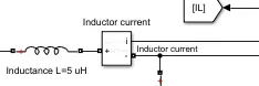
Figure 5. Symbolic representation of Inductor L
Why we select lower value of inductance L ?
> To make the operation in DisContinuous Conduction Mode (DCM)
*********************************************************************************************************************
Design of Capacitance (C):
The role of capacitor in Buck converter is to help ahieve a good output regulation.It is critical to select the right capacitance value. During ON time, the output capacitor gets charged. In this time, the current Ic is enterd to the capacitor. On the other hand, during OFF time, the output capacitor gets discharged. In this time, the current is leaving from the capacitor & it helps to provide the demand of load R.
Peak to peak capacitor voltage is given by,
δVc=δVo = δI /( 8*f*C) ------------------------------- Formula in terms of inductor ripple current 'δI'
δVc=δVo = (Vi * D* (1-D) /( 8*f^2*L*C) ------------Formula in terms of Input voltage 'Vin'
δVc=δVo = (Vo* (1-D)) /( 8*f^2*L*C) ----------------Formula in terms of Output voltage 'Vo'
Let us assume that
Output voltage ripple ∂Vo/Vo = 1% = 0.01;
We have to design the output capacitor such that the output voltage ripple is less than 1%. i.e.
δVo/Vo = 0.01
Therefore, minimum value of output capacitance Cout is given by,
Cout = (1-D)/ (8*f^2*L*(δVo/Vo)) ---------------------------------------Formula
Cout = (1-0.25) /( 8*10*10*10^6*5*10^-6*0.01) = 18.75 milli--Farad
Minimum value of Capacitance Cout = 18.75 mF
During OFF time, the capacitor helps to prevent the regulation from falling too much. Therefore, the capacitance should be high to maintain the desired regulation or ripple voltage.
Take, capacitance of the capacitor is given by,
Capacitance Cout = 19 milli-Farad
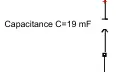
Figure 6. Symbolic representation of capacitor C
As the capacitor is connected in parallel with load resistance R, thus the voltage across capacitor is same as that of load voltage & it is equal to 5 volt.
********************************************************************************************************************************
Input & Output Power
Power :
The product of voltage & current gives the power. Mathematically,
Input Power is given by
Input power (Pin) = Input voltage (Vin) * Input current (Iin)
Pin = 10 * 50 = 500 watt
Input Power Pin = 500 watt
Output power is given by
Output Power (Pout) = Output Voltage (Vout) * Output current (Iout)
Pout = 5* 20 = 100 watt
Output Power Pout = 100 watt
Practically, the output power is always less than input power because due to some switching losses, we get less power at its output side.
Here, we can calculate the switching losses as
Switching losses = Input power (Pin) - Output Power (Pout) = 500 - 100 = 400 watt.
Figure 7 shows the block digram of power & input,output power waveform.
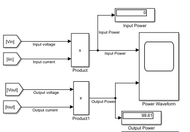
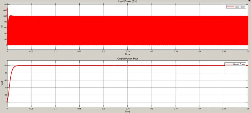
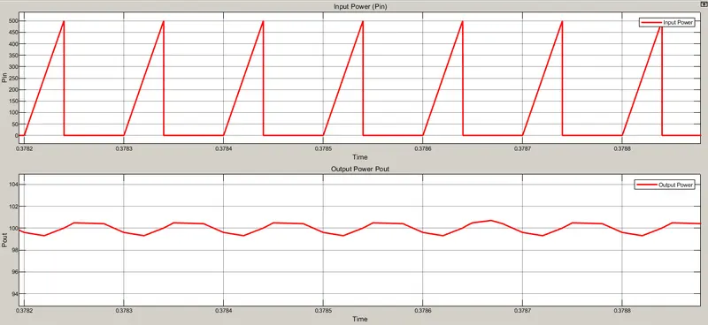
Figure 7. Input & Output Power Waveform of BUCK Converter in DCM ( Zoom out & Zoom In)
*************************************************************************************************
Closed Loop Feedback system
Practically, the output voltage must remains constant to give smooth operation of any electrical device. But due to the variation in input voltage, the output voltage also varied. To avoid the variation in output voltage, we must require to maintain it in constant level. For this reason, we design a closed loop feedback system. In which we compared the actual output voltage to the reference voltage. Here the reference voltage is 30 volt. Both reference voltage as well as actual output voltage is given to the error block ( Sum Block) as a input. This error block gives the diffence between two voltages as an output. The output of error block is given to the PI Controller. PI (Proportional,Integral) Controller is a special type of controller in control system which is widely used in industry & it creates an output which is given to the PWM ( Pulse Width MOdulation) Generator block. Then after this PWM generator genrate duty cyccle for a switch (MOSFET) so that the output voltage must remains constant during any input variation. But the input voltage variation is always greater than output voltage i.e. 5 volt because this converter acts as a BUCK in which the input voltage must be greater than output voltage. Figure 8 shows the block diagram, PI controller input, output as well as duty cycle of BUCk convereter.
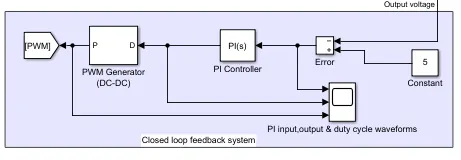
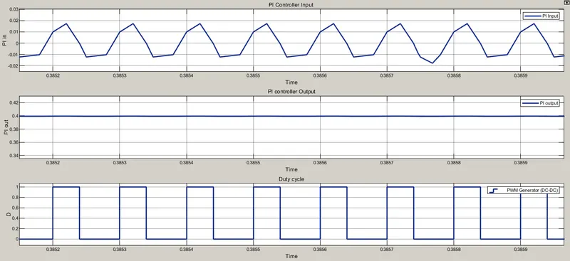
Figure 8. Closed loop feedback system for BUCk Converter in DCM
*****************************************************************************************
Working of Buck Converter in DCM
The BUCk converter in DCM operate in three modes of operation:
1) ON mode of operation:
When switch is ON, the input is connected to the output side, the voltage across switch is zero and voltage across diode is neagtive of input voltage. The turn on voltage Vin-Vout. In Buck converter, the inductor L is connected in series with input as well as output & therefore it stores some energy during this time ON interval.
Inductor current start increasing to peak value ( Inductor charged)
2) OFF mode of operation before inductor fully discharge:
When switch is OFF, the output is disconnected from input side, the voltage across switch appears and is equal to input voltage. During this interval, inductor L supply their stored energy to load resistance to maintain the constant output voltage when input is cut off.This inductor current complete their path through load R & schottky diode & inductor discharge completely & reaches to zero.
Inductor current start decreasing towards zero value ( Inductor discharged)
3) OFF mode of operation after inductor fully discharge:
When the inductor completely discharged, it stays at zero level for short interval of time. That means the switch is turned off completely & tha value of inductor current ramians constant which is equal to 0 ampere.
Inductor current stays at zero ( Inductor completely discharged)
Figure 9 & 10 shows the MOSFET voltage, current waveform & diode voltage, current waveform.
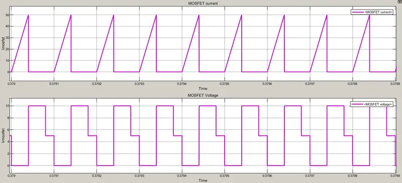
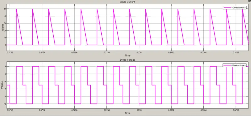
Figure 10. Diode current & Voltage waveform of BUCK converter in DCM
When we run the above simulink model, we get different waveforms like input, output voltage waveform, inductor current waveform, input, output power waveform, MOSFET voltage, current waveform, Diode voltage, current waveform, PI controller input, output waveform & PWM (pulse) waveforms we have seen above individually.
when the switch is turned ON:
MOSFET current : 0 to 50 ampere;
MOSFET Voltage : 0 volt;
Diode current : 0 ampere;
Diode Voltage : decreases from -5 to -10 volt;
when the switch is turned OFF but inductor does not fully discharged:
MOSFET current : 50 to 0 ampere;
MOSFET Voltage : Decreases from 10 to 5 volt;
Diode current : 0 to 50 ampere;
Diode Voltage : increases from -10 to 0 volt;
when the switch is turned OFF & inductor fully discharged:
MOSFET current : 0 ampere;
MOSFET Voltage : Decreases from 5 to 0 volt;
Diode current : 0 ampere;
Diode Voltage : Decreases from - to -0 volt.
***************************************************************************************
Simulation Results : Input & Output VOltage WAveform:
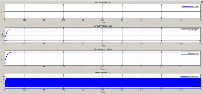
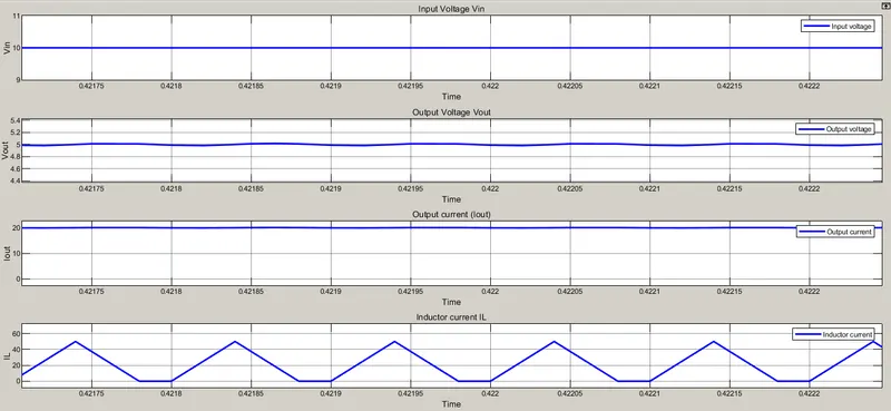
Figure 11. Input & Output voltage, Output current & inductor current waveform
From above figure 11, we observed that the input voltage is 10 volt which is pure dc while 5 volt is the output voltage which containes a negligible ripple,the output current is nearby equla to 20 ampere which is which is pure dc but the peak value of inductor current is 50 amp which is discontinuous in nature. THis happens due to lower value of inductor present in the above circuit.
*************************************************************************************************************
Different Dynamic Conditions
Suppose, the input voltage is varied. So we will analyse how to affect on our output voltage as well as output power.
Let Input Voltage Vin = 15 volt;
Simulation Result:
Figure 12. Input, output voltage & output current,inductor current waveform with 15 volt input voltage supply
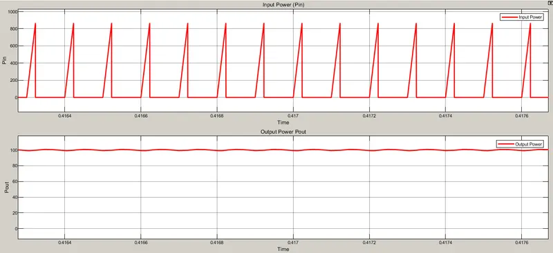
Figure 13. Input & Output Power Waveform with input voltage 15 volt dc.
Let Input Voltage Vin = 20 volt;
Simulation Result:
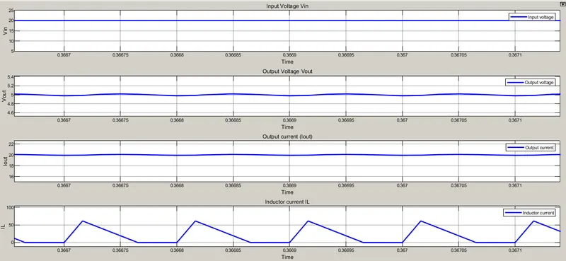
Figure 14. Input, output voltage & output current,inductor current waveform with 20 volt input voltage supply
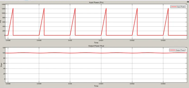
Figure 15. Input & Output Power Waveform with input voltage 20 volt dc.
From above figure 12,13,14 & 15, we observed that when the input voltage increases, the turn ON time i.e. charging time decreases but the turn off time i.e. discharge time of inductor increase. The output voltage as well as output current is same of all dyanmic conditions with constant output power 100 watt.
Comment:
> Buck Converter step down the input voltage
> Whenever the input voltage gets changed, the output voltage & output power remains constant.
> BUCK converter operated in DCM mode gives lower efficiency because, the switch is not continuously connect input & output side & thus reduce to improve efficiency.
> BUCK converter in DCM require low value of filter circuit i.e. Inductor L and hence to reduce the size of circuit & cost as well.
**********************************************************************************************************************************************
**********************************************************************************************************************************************
Project Number : 3
Boost Converter in CCM
Input Voltage : 20-30 volt ; Output Voltage: 40 volt ; Power level: 600 watt
Objective of Step-up converter (Boost Converter):
Our main objective is to design a dc-dc converter such that the conveter should convert 20 to 30 Volt from the battery pack to the the 40 Volt loads with power level 600 watt. For this purpose, we want to use the step up chopper. With the help of this chopper, we can easily convert low input dc voltage to the high dc output voltage.The circuit diagram of boost converter is shwon in figure 1 with LC filter & Resistance R as a load.
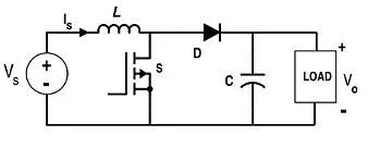
Figure 1. Circuit diagram of Boost Converter
In Boost converter, the inductor L is connected to the source side & it supplies the stored energy during the switch OFF. We want to design such a Boost converter in CCM which convert 20-30 volt input dc voltage to the 40 volt dc with output power 600 watt. This is shown in simulink model of figure 2.
Simulink Model of Boost Converter:
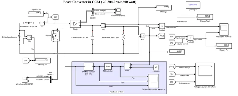
Figure 2. Simulink model of Boost Converter in CCM
Construction & working principle of Boost Converter in CCM:
In above figure, we seen that input voltage is connected in series with inductor L whose effective inductance is calculated as follows. The value of inductance is 0.4 milli-henry. Here, the inductor L is connected in series with input voltage source therefore the current flowing through the inductor is same as input current. The second terminal of inductor L is connected to the drain terminal of MOSFET and anode terminal of diode. Here we are using MOSFET acts as a switch bacause the voltage drop across MOSFET is less as compared to other switching devices. The source terminal is connected to the negative terminal of input votlage source. The gate terminal is connected to the PWM Generator block as shown in above figure. The cathode terminal of schottky diode is connected to the parallel RC circuit in which the value of capacitance C is 2 milli-farad & load resistance 2.7 ohm.
Some times the input voltage is not a constant but we want to obtain constant output voltage with constant output power also. Therefore, for which we designed a closed loop feedback circuit in which actual output voltage compares with reference voltage. Here reference votlage set to 40 volt. The difference in both these voltages is given to the PI controller, the PI controller make such an output so that PWM generate an acuurate duty cycle to the switch.This is shown in dark curved area as shown in above figure.
When switch is triggered by providing gate signal to MOSFET,the current flowing through the DC voltage source- Inducctor L- & MOSFET. During this period, the inductor L stored some energy. When switch is turned OFF, the output side is connected to the input side, & hence in this case, the the inductor supplies their stored energy to the load to boost up the voltage & thus we get higher output voltage than input voltage. To operate the converter in CCM, the value of inductance should be higher.
Before running this simulation, it is necessary to know the value of inductance L, capacitance C, switching frequency F, duty cycle D, etc. It is shown below.
Design Parameters:
Input Voltage Vin: 20-30 volt;
Output voltage Vout : 40 volt;
Output Power Pout : 600 watt.
1) Duty cycle of Boost Converter :
For Boost converter, duty cycle is given by
Vout / Vin = 1 / (1-D) ----------------------------------------------Formula
If Vin = 30 volt;
40/30 = 1/ (1-D)
D = 0.25
If Vin = 20 volt;
40/20 = 1/ (1-D)
D = 0.5
Duty Cycle D = 0.25 to 0.5
that means, the MOSFET is turned ON for time interval between 25 to 50 %. This is shown in following waveform 3.

Figure 3. Duty cycle of PWM Generator
From above waveform 3, we observed that for input voltage 20 volt, we got 50 % duty cycle to be turned ON of 50 % to be turned OFF.
2) Switching Frequency F:
Let us assume that the switching frequency should be 10 kilo-Hertz & set to 10 kHz in PWM Generator block as shown in figure 4.
Figure 4. PWM Generator block showing switching frequency
3) Design of Load Resistance R:
In Boost converter, the load resistance is represented as R and its value can be calculated as follows & its block diagram is shown in figure 5.
Resistance R = (Output Voltage) ^2 / Output power ---------------------------------Formula
R = 40*40/600 = 2.67 ohm
Load Resistance R = 2.7 ohm
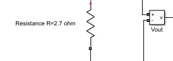
Figure 5. Load Resistance R
4) Design of Inductance L :
Inductance is one of the most important circuit in Boost converter, it performs an operation during switch Turned OFF. The value of inductance can be calculated as follows:
Before finding the value of inductance L, it is necessary to know the value of inductor current IL, inductor current ripple ∂IL & it is found as follows:
Input current /output current = 1/ (1-D)
Output current = Output voltage / Resistance = 40/2.7 = 14.82
Output current = Iout = 14.82 Ampere
Input current = output current / ( 1- Duty cycle) = 14.98 / (1- 0.5) = 29.64
Input current = Iin = 29.64 = 30 Ampere
But Input current Iin = Inductor current IL = 30 Ampere
Let us assume that the inductor current ripple ∂IL should be less than 20 %.
Therefore, ∂IL = 0.2 * IL = 0.2 * 30 = 6 ampere
Inductor current ripple = ∂IL = 6 Ampere
Peak Current Rating of Inductance:
Maximum value of inductor current:
Imax = IL + ∂IL/2 = 30 +3 = 33 Ampere
Minimum value of inductor current:
Imin = IL - ∂IL/2 = 30 - 3 = 27 Ampere

Figure 6. Inductor current waveform
Figure 6 shows the inductor current waveform. From this waveform we observed that the inductor current nearby equal to 30 ampere with current ripple is also less than 10%.
Inductance L = Input Voltage * Duty cycle / ( inductor current ripple * switching frequency )
Lcrit = R * (1-D)*(1-D)*D / ( 2 * F) ---------------------------------------------------------------------------------Formula
Lcrit = 2.7*0.5*0.5*0.5 / (2 * 10*1000) = 16.87 * 10^-6 Henry
For Buck Converter in CCM,
L > 1.05 * Lcrit
L > 1.05 * 16.87 = 17.71 uH
Let us assume that the value of inductance is 100 micro Henry.
To reduce the ripple current in inductor current & operate in Continuous COnduction Mode, we select higher value.
Inductance L = 100 uH
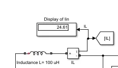
Figure 7. Block diagram of Inductor L
5) Design of Capacitance C:
Let us assume that the output voltage ripple should be less than 1 %.
i.e. ∂Vo/Vo = 1% = 0.01
MInimum value of output capacitance for Boost converter in CCM is given by
Cout = D / (R*F*(∂Vo/Vo)) ---------------------------------------------------------------------Formula
Cout = 0.5 / (2.7*10*1000*0.01) = 1.85 milli-Farad = Say 2 mF
Capacitance C = 2 mF
Block diagram of capacitor is shown in figure 8.
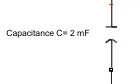
Figure 8. Block diagram of Capacitor C
The voltage across capacitor is same as that of output voltage & equal to 40 volt.
Simulation Result:
When we run above simulink model, we obtain following waveforms like, input,output voltage, input, output power, MOSFET votlage, current & Diode voltage & current waveform as shown in following figures.
Output Voltage Waveform:
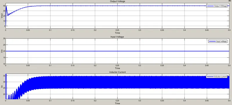
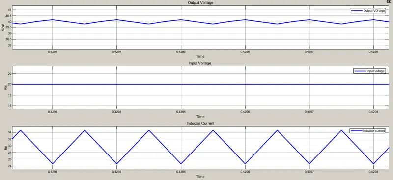
Figure 9. Input,Output Voltage waveform & Inductor current waveform for Boost converter in CCM (Zoom Out & Zoom In)
From above figure 9, we observed that for input voltage 20 volt dc, we got 40 volt at its output side with very low voltage ripple less than 1%. The inductor current value is near by equal to 30 Ampere which is continuous in nature.
Power Waveform:
Input power = Input voltage * Input current
Pin = 20 * 30 = 600 watt
OUtput power = Output voltage * Output current
Pout = 40 * 14.82 = 592.8 watt
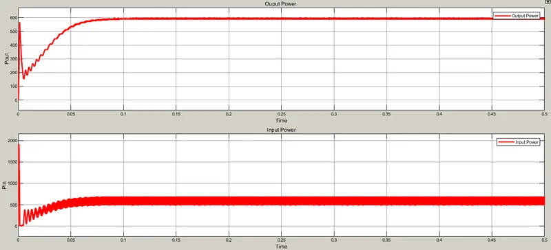
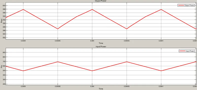
Figure 10. Output & Input power of Boost converter in CCM
From above waveform of power, we observed that the input power is 600 watt & output power is nearby equal to 600 watt i.t. 594 watt.Practically, it happens due to switching losses, the output power should be less than input power.
MOSFET Voltage & current Waveform:
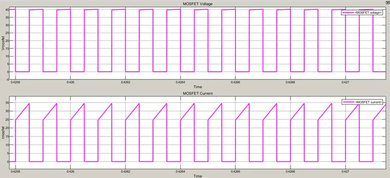
Figure 11. MOSFET Voltage & current waveform
From above figure 11, we can say that the voltage across MOSFET is 40 volt which is equal to output voltage, because the Switch is connected in parallel with load in we know that the voltage is same in parallel circuit. The average value of MOSFET current is nearby equal to 15 to 17 ampere. During Switch ON, the voltage across switch is zero, while when switch is OFF, the voltage across switch is maximum and equal to Vout.
Diode Voltage & Current waveform:
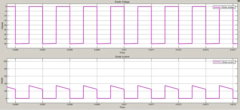
Figure 12. Diode Voltage & current waveform
From above waveform, we can say that the voltage across diode is -40 volt during ON time and voltage is zero during OFF time. When switch is OFF then & only then diode conducts otherwise it will not conduct because the switch has low resistance than diode resistance & hence the current alway obey low resistance path.
When Swich is ON:
MOSFET Voltage : 0 volt;
MOSFET Current : Higher say 35 ampere peak;
Diode Voltage : -40 volt;
Diode Current : 0 Ampere
When Swich is OFF:
MOSFET Voltage : 40 volt;
MOSFET Current : 0 ampere;
Diode Voltage : 0 volt;
Diode Current : higher say 15 Ampere
PI Controller Input-Ouput waveform & PWM pulse:
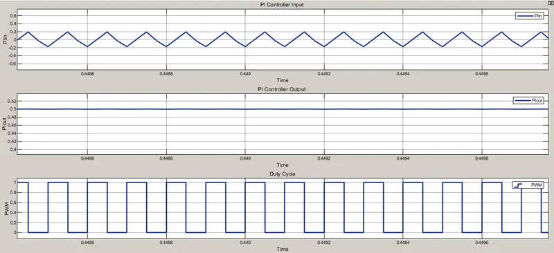
Figure 13. PI Controller Input, Output waveform & duty cycle of switch
From above figure, we observed that the input of PI controller is 0.2 volt with output 0.5. The duty cycle is 50%.
Different Dynamic Conditions:
Suppose, the input voltage is varied. So we will analyse how to affect on our output voltage as well as output power.
Let Input Voltage Vin = 25 volt;
Simulation result:
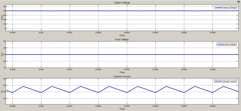
Figure 14. Input, output voltage & inductor current waveform with 25 volt input voltage supply
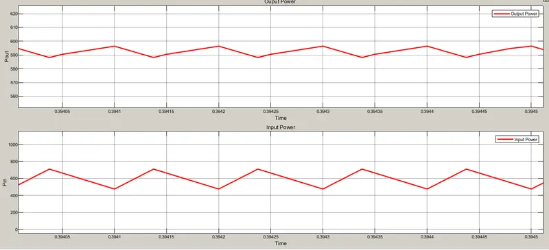
Figure 15. Input & Output Power Waveform with input voltage 25 volt dc.
Let Input Voltage Vin = 30 volt;
Simulation result:
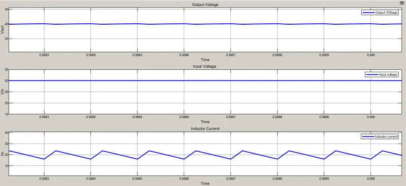
Figure 16. Input, output voltage & inductor current waveform with 30 volt input voltage supply
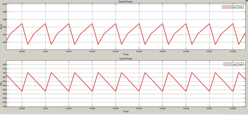
Figure 17. Input & Output Power Waveform with input voltage 30 volt dc.
From above figure 14,15,16 & 17, we observed that whenever the input voltage gets varried, the output voltage remains constant & equal to 40 volt with constanct output power near by equal to 600 watt. As the voltage increases, the duty cycle gets decreses & inductor charge immediately. That means, the turn ON time is less than turn off time.
Comment:
> Boost Converter step up the input voltage
> Whenever the input voltage gets changed, the output voltage & output power remains constant.
**********************************************************************************************************************************************
**********************************************************************************************************************************************
Project Number : 4
Boost Converter in DCM
Input Voltage : 5-10 volt ; Output Voltage: 12 volt ; Power level: 150 watt
The procedure is same as that of Boost convrerter in CCM, but the difference in the value of inductance.
For Boost converter in DCM, take the value of inductance should be less than critical value of inductance.
1) Design of load resistance R:
For boost converter, Duty cycle is given by
Vout / Vin = 1/(1-D) = 0.67
Duty cycle D = 0.67
R = Vout^2/Pout = 12*12/150 = 0.96 ohm
Load Resistance R = 0.96 ohm
Let us assume that the switching frequency should be 10 kHz.
Switching frequency F = 10,000 Hz
2) Design of Inductance L :
Inductance L = Input Voltage * Duty cycle / ( inductor current ripple * switching frequency )
Lcrit = R * (1-D)*(1-D)*D / ( 2 * F) ---------------------------------------------------------------------------------Formula
Lcrit = 0.96*0.33*0.33*0.67 / (2 * 10*1000) = 3.5 * 10^-6 Henry
For Boost Converter in DCM,
L < 1.05 * Lcrit
L < 1.05 * 3.5 *10^-6 = 3.675 uH
Let us assume that the value of inductance is 2 micro Henry.
To operate in Disontinuous Conduction Mode (DCM), we select lower value.
2) Design of Capacitance C:
Let (∂Vo/Vo) = 1% = 0.01
Cout = D/ R*F*(∂Vo/Vo) = 0.67 / (0.96*10*1000*0.01) = 7 milli-Farad
Capacitance C = 7 mF
Simulink Model:
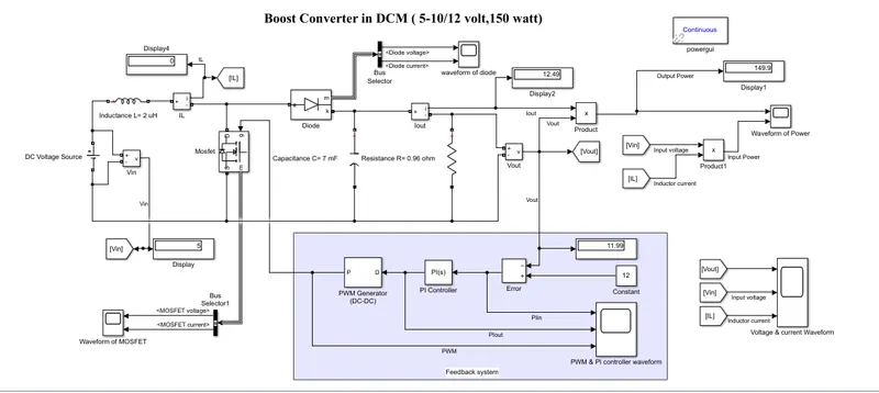
Figure 1. Simulink model of Boost Converter in DCM
The construction & working principle of Boost converter in DCM is same as that in CCM, but only difference in the values of input voltage,output voltage, output power, duty cycle, inductance L, load resistance R, capacitance C value only. When we run above simulink model, we got following output waveforms as follows:
Simulation Result:
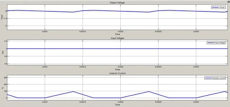
Figure 2. Input, Output Voltage & Inductor current waveform
Figure 2 shows the input,output & inductor current waveform. In wahich we observed that for 5 volt of dc input we got 12 volt at its output voltage with inductor current is 100 ampere peak in discontinuous mode.
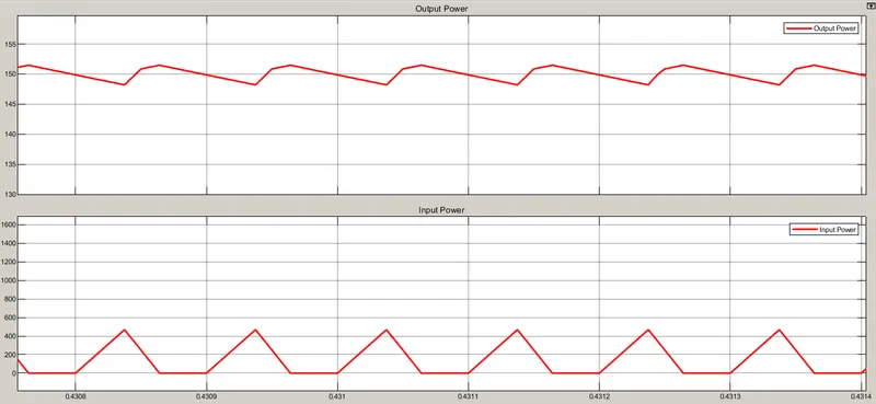
Figure 3. Input & Output Power waveform
From above figure,we we observed that output power is 150 watt with input power nearby equal to 225 watt. Remaining power should be losses.
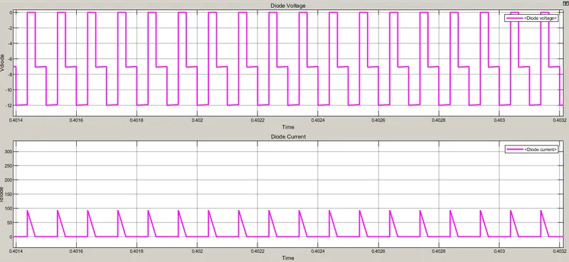
Figure 4. Diode Voltage & Current waveform
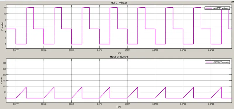
Figure 5. MOSFET Voltage & Current waveform
From above figure 4 & 5, we can say that when switch is ON, the voltage across diode is -12 volt & voltage across switch is zero. When switch is OFF,vice versa. Boost converter in DCM, operate in three modes- ON mode, OFF before inductor is not fully discharged & OFF mode after inductor fully discharged.
*********************************************************************************************
***********************************************************************************************************