Project 1 - Loss calculation for a DC/DC converter-MATLAB
---- PROJECT 1 ----
PROJECT REPORT -
1. Power electronics:
The power electronics is all about the application of electronics devices which are utilized for power conversion like power electronics can be basically used for rectification and inverting applications, power electronics in this modern age, used for controlling or for converting power supply to the desired level.
Advantages of power electronics:
-> High efficiency and reliability due to low losses occurrence
-> Fast dynamic response and have long life
-> They have small size, thus weight results in less space required for them
Applications of power electronics:
-> Electrical vehicles
-> Transmission systems
-> Motor drive systems
1.1 Main types of power converters:
* Boost converter
* Buck converter
* Buck-Boost converter
1.1.1 Boost converter:
The boost converter is a type of converter which is used to step-up converter. It is used to increase the DC input voltage to desired value of the DC output signal value. The DC output signal can be adjusted by the potentiometer and the DC output signal can be depended on the circuit inductor and capacitor design and selection.
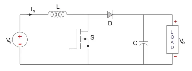
fig(a) Boost converter circuit
1.1.2 Buck converter:
The buck converter is a type of converter which is used to step-down converter. It is used to decrease the DC input voltage to desired value of the DC output signal value. The DC output signal can be adjusted by the potentiometer and the DC output signal can be depended on the circuit inductor and capacitor design and selection. It is exact opposite to the boost converter’s operation.
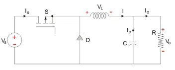
fig(b) Buck converter circuit
1.1.3 Buck-Boost converter:
The buck boost converter’s name suggests the operation, as its operation is like the combine operation of the buck and boost converter. The buck-boost converter produces a DC output voltage that can be either bigger or smaller in magnitude than the DC input voltage.
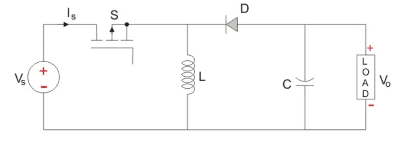
fig(c) Buck-Boost converter circuit
2. Boost converter:
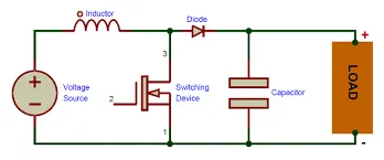
fig(a) Boost converter circuit
2.1 Operation of Boost converter:
When MOSFET power switch turns ON then the inductor sees a nearly constant DC voltage Vin across it and so the current in the inductor ramps up linearly. When the MOSFET power switch turns OFF then since the current in the
inductor cannot be nullified instantaneously, it charges up the drain mode of the MOSFET and keeps charging it until it cap voltage reaches a diode voltage higher than whatever output voltage on Vout exists. At this time the diode turns
ON and the inductor current starts charging the output capacitor. For the inductor current to decrease the Vout plus a diode voltage should be more than Vin so that the inductor sees a DC voltage of Vout+Vd-Vin across it with the
drain of the MOSFET being positive. This causes the inductor current to ramp down linearly. Now by controlling the ON time and OFF time of the power switch we can control the average current in the inductor and hence create a boost
converter which may regulate the average input current and the output voltage. Hence in this way the input DC voltage is been controlled and increase from the boost converter.
3. IMPORTANT PARAMETER VALUES
VOLTAGE INPUT = 24V
VOLTAGE OUTPUT = 48V
CURRENT OUTPUT = 3.265A
INDUCTOR VALUE = 0.006H
CAPACITOR VALUE = 4.13x10^-5F
RESISTIVE LOAD = 15 OHMS
SWITCHING FREQUENCY = 20KHz
DUTY CYCLE = 0.5
OUTPUT CAPACITOR = 100pf
DIODE RESISTANCE = 25 mΩ
CAPACITOR RESISTANCE = 40mΩ
4. Losses of Boost converter:
The boost converter has two types of losses in it. The types of losses of boost converter are listed below.
4.1 Switching losses:
These switching losses are considered as the power losses when the current is being switched between the power switch. These losses are basically the switching losses because of these switching losses occurs when there is power devices swtiching occurs.
4.2 Conduction losses:
These losses are the power dissipated in the circuit elements when the current is flowing through them. These conducting losses occurs when there is conduction takes place through the circuitary elements of the boost converter.
5. Losses Calculations:
5.1 Switching losses:
These switching losses can be obtained as listed in the following.
Switching losses = Fs x Co x Vo^2
where
Fs = Switching frequency
Co = Output capacitor
Vo = Output voltage
Switching losses = Fs x Co x Vo^2
Switching losses = 20000KHz x 100pf x 48^2
Switching losses = 20000 x 1.0×10^-10F x 2304V
Switching losses = 0.04608 W
5.2 Conduction losses:
These Conduction losses are divided as listed in the following. As this conducting loss are considered as the circuitry components used in the converter.
-- Inductor losses
-- Diodes losses
-- Capacitor losses
A) Inductor losses:
This inductor losses occured and considered at the inductor used in the boost converter. The inductor losses can be obtain as discussed in the folllowing.
Inductor losses = I^2R
Inductor current (rms) = Io√{(D)/(1-D)}
where
Io = Output current
D = Duty cycle
R = Resistance of inductor
Inductor losses = Io√{(D)/(1-D)}
Inductor losses = 3.265A √ {(0.5)/(1-0.5)}
Inductor losses = 3.265 x √ 1
Inductor current (rms) = 3.265 A
Inductor resistance = 0.3Ω*
Inductor losses = I^2R
Inductor losses = 3.265^2 x 0.3
Inductor losses = 3.19 W
B) Diode losses:
The diode losses are basically of types. This loss can be describes as I^2.R losses.
Diode losses = I^2R
Diode current (rms) = [Io/√(1-D)]
where
I = Diode Current
R = Diode resistance = 25 mΩ = 0.025 Ω
Diode current (rms) = [Io/√(1-D)]
Diode current (rms) = [3.265/√(1-0.5)]
Diode current (rms) = [3.265/0.707]
Diode current (rms) = 4.618
Diode losses = I^2R
Diode losses = 4.618^2 x 0.025Ω = 0.533 W
Diode losses = 0.533 W
C) Capacitor losses:
The capacitor losses are considered as the losses which occurs at the capacitor of the boost converter. The boost converter's capacitor losses are discussed in the following
Capacitor losses = I^2R
where
I = Current
R = Capacitor resistance = Cesr = 40mΩ = 0.040Ω*
Capacitor losses = 3.625^2 x 0.040Ω = 0.525625 W
Capacitor losses = 0.525625 W
5.3. Calculation of total power losses:
Total power losses = Switching losses + Inductor losses + Diode losses + Capacitor losses
Total power losses = 0.04608 W+ 0.533 W+ 3.19 W +0.525625 W
Total power losses = 4.29408 W
6. Calculation of Efficiency by means of total power losses:
Efficiency = Output/Input
Efficiency = (Output)/(Output + losses)
Efficiency = 48V / 48V + 4.29W
Efficiency = 48V / 52.29
Efficiency = 0.917
Efficiency = 91.7%
7. Inductor design for boost converter:
As to design the inductor for the boost converter there are some formulas for calculating the accurate the value of inductor of the boost converter. For selection of the inductor we need to determine the switching frequency, Duty cycle of the converter, Input voltage, and the ripple current as well.
Inductor design of boost converter = [(D/Fs) x Vi] / Ripple current
where
D = Duty cycle = 0.5
Fs = switching frequency = 20KHz
Vi = INput voltage = 24V
The inductive ripple current is considered as 10%
Ripple current = 10%
Inductor design of boost converter = [(0.5/20KHz) x 24V] /10%
Inductor value = [0.0006] / 10%
Inductor value = 0.006 H
8. Capacitor design for boost converter:
The converter has external compensation, any capacitor value which is the recommended minimum in the datasheet can be used, but the compensation has to be adjusted for the used output capacitance. The capacitor design is also important in the boost converter. For selection of the capacitor we need to determine the switching frequency, Duty cycle of the converter, output current, and the output voltage ripple as well.
Capacitor design of boost converter = [(Io x D)/(Fs x ΔVo)]
where
Io = output current of the converter = 3.26 A
D = duty cycle = 0.5
Fs = switching frequency of the converter = 20KHz
ΔVo = output voltage ripple = [ESRx(Io/1-D)+(ΔIl/2)]
Here the Output voltage ripple can be determined from the above discussed formula
ΔVo = output voltage ripple = [ESRx(Io/1-D)+(ΔIl/2)]
where
ESR = equivalent series resistance of the used output capacitor = 0.3
Io= maximum output current of the application = 3.26
D = duty cycle = 0.5
ΔIL = inductor ripple current = 10%
ΔVo = output voltage ripple = [0.3x(3.26/1-0.5)+(10%/2)]
ΔVo = output voltage ripple = 1.935V
Capacitor design of boost converter = [(Io x D)/(Fs x ΔVo)]
Capacitor design of boost converter = [(3.2Ax 0.5)/(20KHz x 1.935V)]
Capacitor design of boost converter = [1.6/38700]
Capacitor design of boost converter = 4.13 x 10^-5
9. Project Simulation model:
SIMULATION VALUES
VOLTAGE INPUT = 24V
VOLTAGE OUTPUT = 48V
INDUCTOR VALUE = 0.006H
CAPACITOR VALUE = 4.13x10^-5F
RESISTIVE LOAD = 15 OHMS
SWITCHING FREQUENCY = 20KHz
DUTY CYCLE = 0.5
Here I had also simulated a model on the BOOST converter design. The below model is designed for the boost converter where the duty ratio is 0.5, where input voltage is 24V and output voltage is 48V. This model is designed based on the above simulation values.
Design of BOOST converter with 24V input and 48V output values:
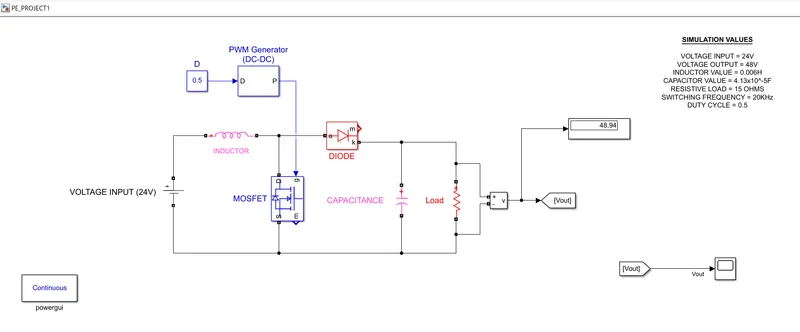
fig(a) Boost converter with 24v to 48v step-up converter
Output scope of the boost converter where the amplitude is at 48V:
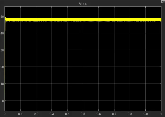
Fig(b) Output scope of 48V from the boost converter.
10. CONCLUSION:
Hence all the requierments are met. From the above project, I had concluded that the boost converter i.e. DC-DC converter have good efficiency rate like the transformer efficiency. After utilsing the losses from the boost converter to obtain the efficiency, the efficiency is almost 91%. To obtain the losses, I had considered the both losses which are switching losses and conduction losses.IN the conduction losses there are three types of losses which are inductor losses, capacitor losses, diode losses. The conduction losses are the losses which includes the components used in the boost converter. After obtaining the efficiency of the boost converter, I had designed a boost converter, in which it has 0.5 of duty ratio where 24V input is given to the system and 48V DC output is obtain at the load side. So this system is accurate according to the duty ratio, the inductor design and capacitor design are also complied and acuurate values are obtained from the therotical calculations. Hence the design of boost converter is also acurate.
------THANK YOU------