Project 1 - Loss calculation for a DC/DC converter-MATLAB
- Extending the learned lessons in previous module, you will be diving into another power electronics concept on your own.
- Design of boost converter, and calculating the loss of different components including power switching device and deriving efficiency of boost converter. This is applicable in power supply industry, electric vehicles etc where DC-DC converter is required to boost the voltage from DC source. All the aspects of this project with loss calculation, device selection, simulation etc are industry relevant.
calculating the loss of different components including power switching device and deriving efficiency of boost converter
design parameters
Vin=100V
Vout=200V
L=2.5mH
C=50uF
R=10ohm
Po=4kW
Fs=20kHz
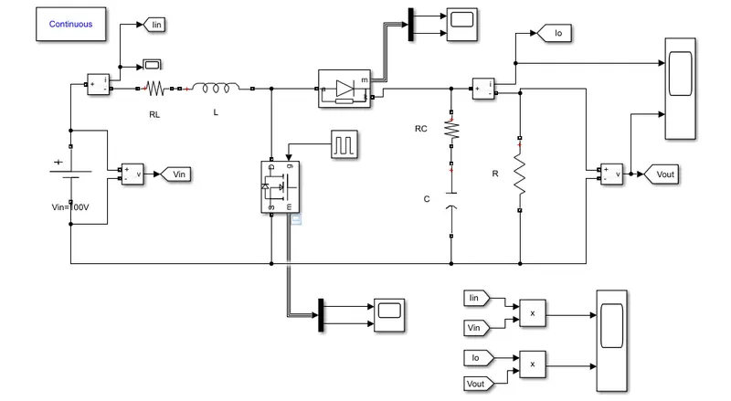
Boost converter design is shown below
To calculate the power loss across inductor and capacitor rL=20mH is connected series with L and rC of 1mH is connected with capacitor respectively.
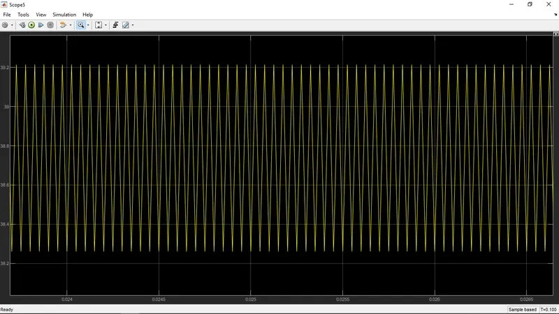
Input current or Inductor current
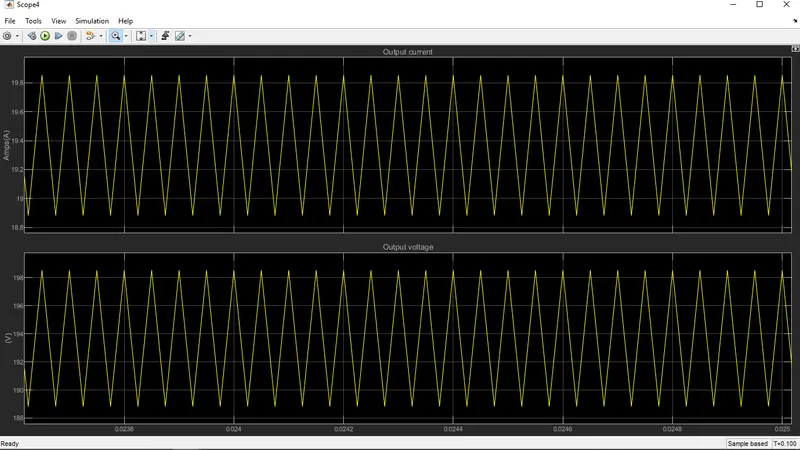
Output current and output voltage
Loss calculation:
DC-DC converters are dynamic systems consisting of the passive components. These components under the effect of thermal stress in a PV system generate power losses. The knowledge of these power losses is necessary to evaluate the conversion efficiency of the system. Using the polynomial approximation method, the equations for calculating losses in the different components were determined.
i)Losses in Mosfet:
The transistor dissipates energy during the firing phase , the conduction phase , and the blocking phase corresponding to a Total energy : per switching period. For a MOSFET, the behavior in conduction regime is similar to that of a resistor, the powers dissipated during this phase and during the switching phases are defined according to following equations:
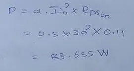
conduction losses in mosfet:

Switching losses in mosfet:
These losses happen as a result of the dissipation in the MOS device when it is not completely OFF and the drain voltage is significant. At this time the MOS device may have lot of current flowing through it with a drain voltage on it thus dissipating a lot of energy. This loss is significant and most of the time cannot be ignored. Let us consider the worst case drain current and voltage of the MOS as shown below:
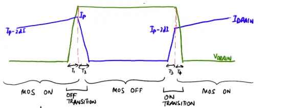

WA: Energy dissipated during the firing phase,
WB: Energy dissipated during the blocking phase,
WCond: Energy dissipated during the conduction phase,
WT: Total energy dissipated by the MOSFET,
RDSon: Source drain resistance of the MOSFET
Vin∶ Voltage at the terminals of the transistor in the blocked state,
In: current delivered by the generator,
IRM: amplitude of the diode's overlay current,
α: the duty cycle, : the switching frequency of the MOSFET,
tcom: duration of the switching phase, and
tBloc: duration of the blocking phase.
the total losses at the MOSFET can be evaluated by:

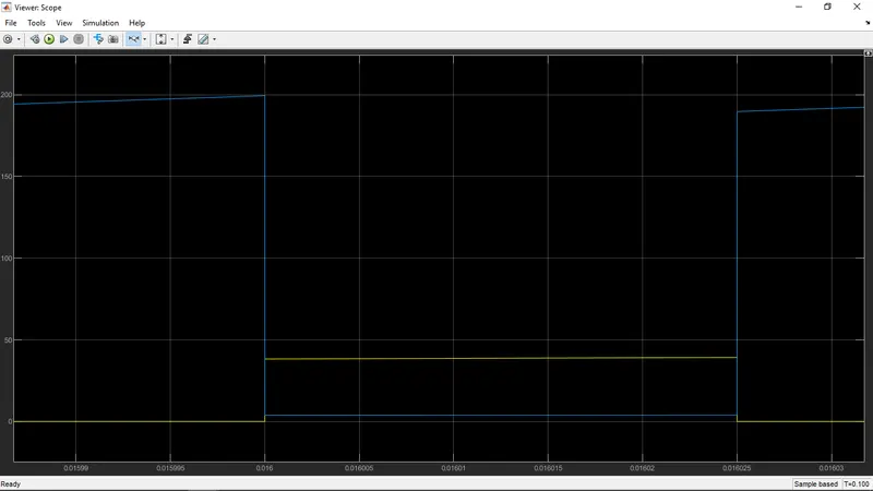
In above plot we can see mosfet voltage and current don't has any delay mean there is no ON or OFF transition losses
So we could neglect switching losses here
finally,mosfet loss here is conduction loss
ii)Losses in Diode:
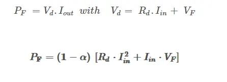
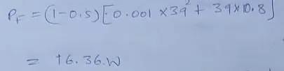
Rd: differential resistance or dynamic resistance
VF: Forward voltage.
iii)Losses in capacitor:
In most cases, a capacitor is a simple capacitance C expressed in Farad but as a component the capacitor is not limited to its simple capacity:
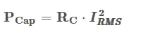
We can rewrite the expression by considering effective currents in the various components of the circuit developed in the ckt:

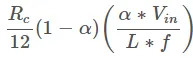 is very very small we can neglect
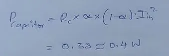
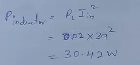
iv)Losses in Inductor:
The equivalent electrical model of a wound inductor can be reduced to an ideal inductor in series with a resistor . The presence of the latter generates direct losses by Joule effect linked to the conductors and to the losses induced in the magnetic core (losses by hysteresis and by eddy currents) which depend on the frequency and the variation of the flux.
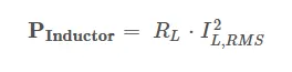
We can rewrite the expression by considering effective currents in the various components of the circuit developed in the ckt:
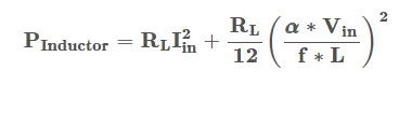
since 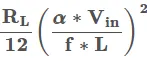 very small ,we can neglect.
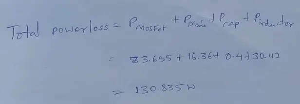
Total power loss:
the constituents of the Boost converter are: MOSFET, Diode, Inductance and Capacitance.
The conversion efficiency can be written as:
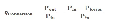
Pin and Pout the powers respectively at the input and output of the converter,
Plosses, the power lost in the converter.
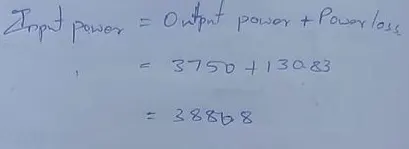
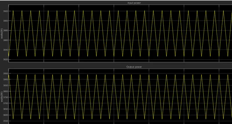
Input power and Output power we can see below
efficiency:
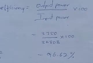
we are getting 96.62%,so the design seems good
almost all losses depends on input current
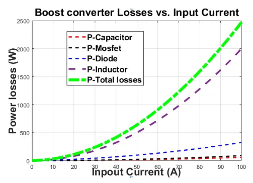
hence efficiency of the converter also depends on Input current
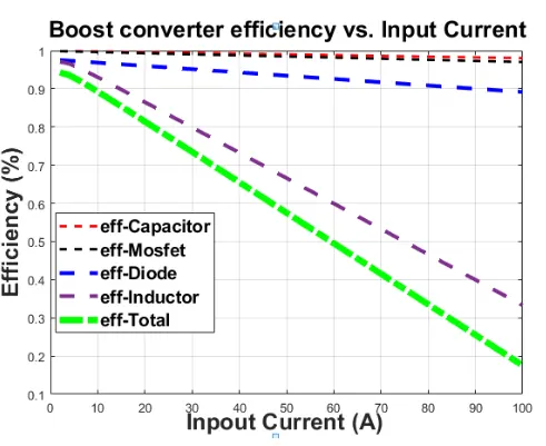
conclusion:
The total efficiency of the converter is strongly influenced by the efficiency of the induction since the efficiency of the capacitor and MOSFET always remain above 95% and 90% respectively. While the efficiency of the diode which is 67% is still acceptable, the induction seems to impose its losses on the converter we simulated. Thus, in order to boost the efficiency of the converter, we must try to work a lot on the effectiveness of the inductor.
The mosfet and diodes are major loss contributors,by using schootky diode power loss at diode can be reduce.