Project 1 - Loss calculation for a DC/DC converter-MATLAB
- Extending the learned lessons in previous module, you will be diving into another power electronics concept on your own.
- Design of boost converter, and calculating the loss of different components including power switching device and deriving efficiency of boost converter. This is applicable in power supply industry, electric vehicles etc where DC-DC converter is required to boost the voltage from DC source. All the aspects of this project with loss calculation, device selection, simulation etc are industry relevant.
I am designing the boost converter for calculating th losses and efficiency of the converter
Boost converter:
A boost converter is a type of DC-DC converter that can step up or boost the voltage of a DC power source to a higher voltage level. It works by storing energy in an inductor during the ON time of a switch and then transferring that energy to the load during the OFF time of the switch.
Boost converter is in on condition:
When a boost converter is in the on condition, the switch (usually a transistor) is closed and the input voltage is applied across the inductor and the switch. As a result, current starts flowing through the inductor and it stores energy in its magnetic field. At the same time, the diode connected in parallel with the load is reverse-biased and does not conduct.
During this on time, the output voltage is equal to the input voltage minus the voltage drop across the switch. The amount of energy stored in the inductor depends on the inductance value, the current flowing through it, and the duration of the on time.
The on time of the switch is controlled by a pulse width modulation (PWM) signal, which determines the duty cycle of the converter. The duty cycle is the ratio of the on time to the total switching period and it is used to regulate the output voltage of the converter.
Boost converter is in off condition:
When a boost converter is in the off condition, the switch (usually a transistor) is open and the energy stored in the inductor is transferred to the load through the diode and the output capacitor. The voltage across the inductor reverses and the energy is released as a voltage pulse.
During the off time, the current flowing through the inductor decreases and the voltage across the diode becomes forward-biased, allowing current to flow through the diode and charge the output capacitor.
The amount of energy transferred to the load depends on the inductance value, the current flowing through the inductor, and the duration of the off time. The off time of the switch is also controlled by the PWM signal, which determines the duty cycle of the converter.
The basic circuit of a boost converter consists of an inductor, a switch (usually a transistor), a diode, a capacitor, and a load. When the switch is turned on, current flows through the inductor and energy is stored in its magnetic field. When the switch is turned off, the energy stored in the inductor is transferred to the load through the diode and the capacitor, resulting in an output voltage higher than the input voltage.
The simulation model is shown below
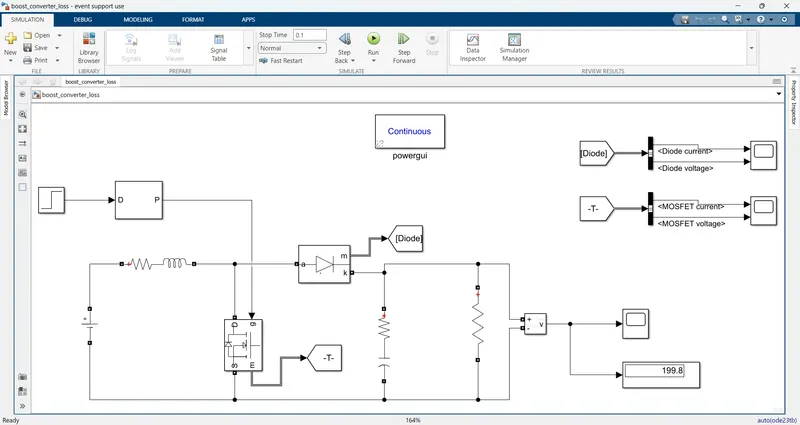
Model explanation
I am taking dc voltage is taken as input and is connected to Rl(parasitic inductance) & L(inductance) and is connected with parallel to diode anode and mosfet switch drain terminal source terminal of the mosfet is connected to dc negative terminal and diode cathode is connected to Rc (parasitc capcitance) & C(capacitance) and is connected to load and is connected to voltage measurement and then scope is connected to voltage measurement.for gate signal i am using pwm generator.
The block parameters are shown below
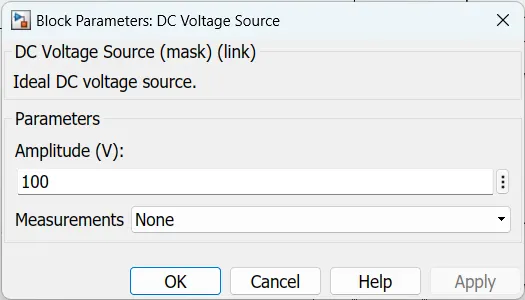
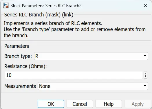
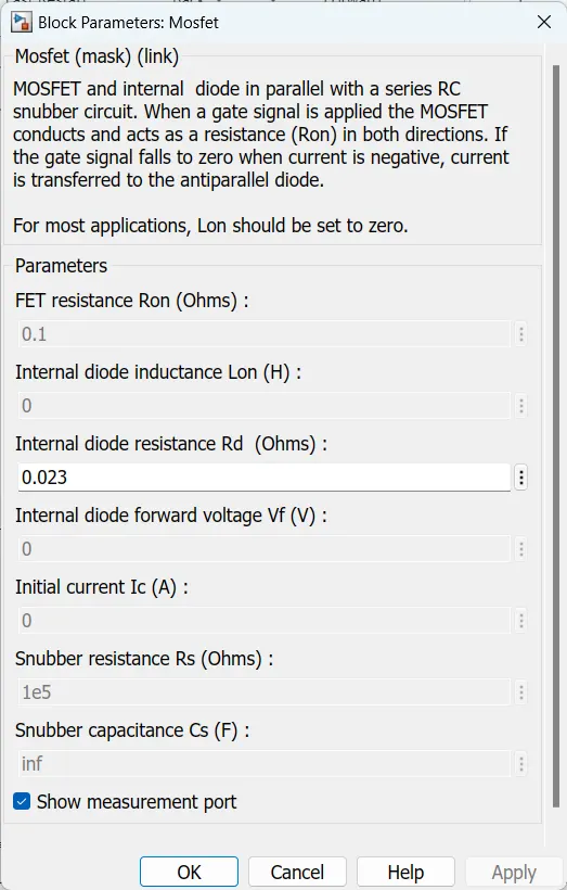
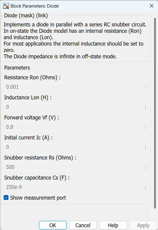
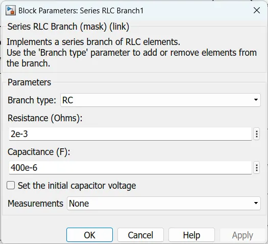
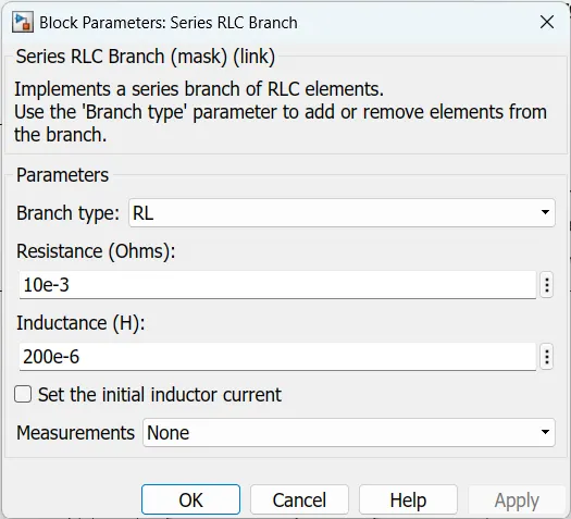
The output voltage is shown below
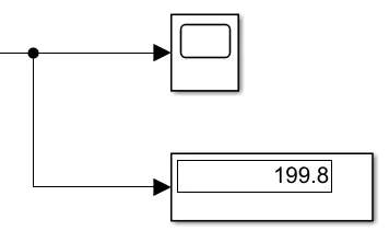
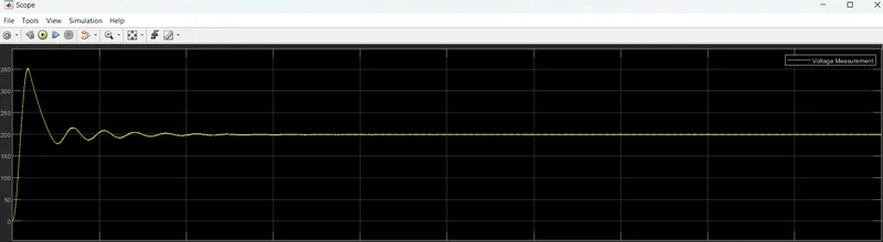
Input voltage is given as 100v and the voltage is stepped up and is come to 200v output.
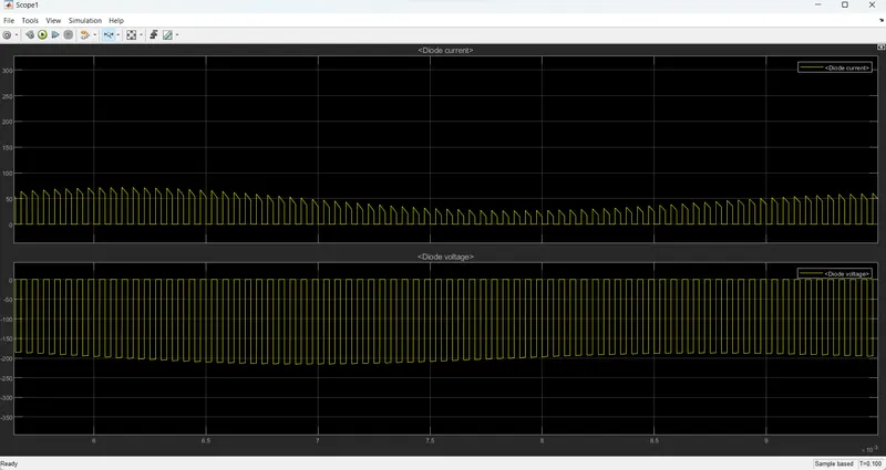
Diode voltage and current is shown below
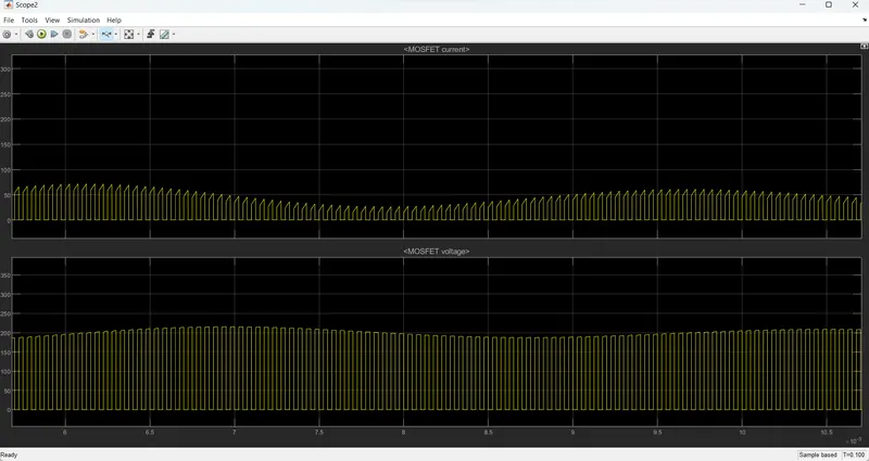
MOSFET voltage and current is shown below
Determining the Losses in Power electronic Converters
In any DC-DC converter majourly consider 4 types of losses are as follows:-
- Conduction Losses
- Diode losses
- Inductor Losses
- Capacitor Losses
Conduction Losses:-
Conduction losses are a result of device parasitic resistances impeding the DC current flow in a DC/DC converter. These losses are in direct relationship with the duty cycle.
When the integrated high-side MOSFET turns on, the load current flows through it. The drain-to-source channel resistance (RDSON) causes power dissipation.
Formula :-
Conduction Losses:- Pc= I² * R *D
here,
p= Power Dissipation
I= Current through MOSFET
R= Resistance in Ohm
D=Duty Cycle= Vout / Vin
Diode losses:-
The diode is forward-biased when the integrated MOSFET turns off. During this time, the inductor current ramps down through the output capacitors, the load and the forward-biased diode. Since the load current is now conducting through the diode, there will be power dissipation in Diode.
This will be calculated by using below Formula:-
Diode Losses:- P= Vf * I* (1-D)
here,
Vf= forward voltage
I= Current output
D=Duty Cycle= Vout / Vin
Induction Losses:-
The conduction losses depend on the load current. With heavier loads, the conduction loss in the MOSFET increases and is the dominating factor. Conduction losses plus switching, driver and internal low-dropout regulator (LDO) losses lead to a considerable generation of heat.
This losses can be calculated by using the below formula:
Pd= I² * R + { (rl / 12) (D* Vin / F*L)}
here,
I= Current output
D=Duty Cycle= Vout / Vi
F= Frequency
L= Inductance value
Capacitance losses:-
While getting the output through the capacitor we can get some power dissipation in capacitor also.
this power dissipation is determined by using the following Formula:-
Pc= {rc* D*(1-D) I² + {rc / 12(1-D)}}*{(D*Vin / C*F)}
here,
I= Current output
D=Duty Cycle= Vout / Vi
F= Frequency
C= Capacitance value
From the given data we can find the losses for Designed DC-DC Converter:-
Vin = 100 V
Vout = 200 V
L = 200uH
C = 400uF
R= 10 Ohms
rL = 10 mOhms
rC = 2 mOhms
rd=5 mOhms
Duty cyclee= 0.5
Conduction Losses:-
Pc= I² * R *D
Iin=Pi/Vi
Pi=V^2/R
Pi=100*100/10=1000
Iin=1000/100
Iin=10A
Pc= (10)² * 0.023*0.5
Conduction losses Pc=1.15W
Diode Losses:- Pd= Vf * I* (1-D)
= 0.8 * 10* (1-0.5)
= 0.8*10*0.5
Diode Losses(Pd) =4w
Inductor Losses:-
PI= I² * R + { (rl / 12) (D* Vin / F*L)}
=1^2*10+{(10*10^-3)(0.5*100/50*200*10^-6)}
=10+{(0.01)(50/0.01)}
=10+50
PI =60 W
Inductor losses=60W
Capacitance Losses:-
Pc= {rc* D*(1-D) I² + {rc / 12*(1-D)}}*{(D*Vin / C*F)}
=2*0.001*0.5*0.5*10^2+(2*0.001*0.5*0.5*100 / 400*50*0.000001)
=0.05+(0.00416/ 0.02)
=0.05+0.208
Capacitance loss Pc=0.258W
Total Losses= Pcon+Pd+Pi+Pc
=1.15+4+60+0.258
Total losses=65.408 W
Efficiency Of Converter:-
The efficiency Of converter is determined by using below formula:
Efficiency = (Pin -Ploss / Pin ) 100
Pin = vin * I
=100 * 10
Pin=1000 W
Efficiency = (Pin -Ploss / Pin )*100
= (1000-65.408 / 1000)* 100
Efficiency = 93.45 %
Results :-
The total Power losses Ploss= 65.408 W
The efficiency of Converter = 93.45 %