Project 1 - Loss calculation for a DC/DC converter-MATLAB
AIM: Design of boost converter, calculating the loss of different components including the power switching device, and deriving efficiency of the boost converter.
(This is applicable in the power supply industry, electric vehicles, etc where a DC-DC converter is required to boost the voltage from the DC source)
THEORY:
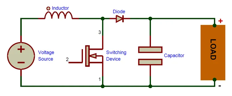
A boost converter is one of the simplest types of switch mode converter. As the name suggests, it takes an input voltage and boosts or increases it. All it consists of is an inductor, a semiconductor switch (these days it’s a MOSFET), a diode, and a capacitor.
working of the boost converter step by step.
STEP – 1:The output capacitor is charged to the input voltage minus one diode drop.
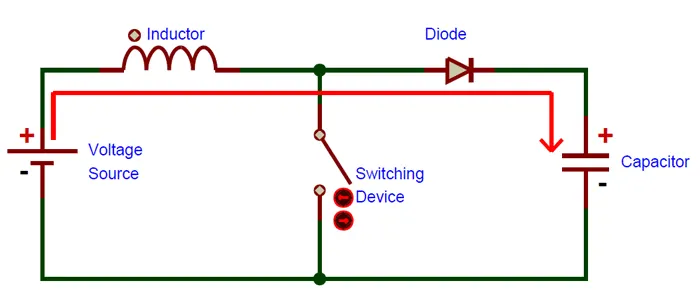
STEP – 2
Now, it’s time to turn the switch on. Our signal source goes high, turning on the MOSFET. All the current is diverted through to the MOSFET through the inductor. Note that the output capacitor stays charged since it can’t discharge through the now back-biased diode.
The power source isn’t immediately short-circuited, of course, since the inductor makes the current ramp-up relatively slowly. Also, a magnetic field builds up around the inductor.
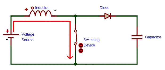
STEP – 3
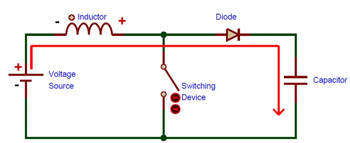
The MOSFET is turned off and the current to the inductor is stopped abruptly.
The very nature of an inductor is to maintain smooth current flow; it doesn’t like sudden changes in current. So it does not like the sudden turning off of the current. It responds to this by generating a large voltage with the opposite polarity of the voltage originally supplied to it using the energy stored in the magnetic field to maintain that current flow.
If we forget the rest of the circuit elements and notice only the polarity symbols, we notice that the inductor now acts like a voltage source in series with the supply voltage. This means that the anode of the diode is now at a higher voltage than the cathode (remember, the cap was already charged to supply voltage in the beginning) and is forward-biased.
The output capacitor is now charged to a higher voltage than before, which means that we have successfully stepped up a low DC voltage to a higher one!
These steps happen many thousands of times (depending on the frequency of the oscillator) to maintain the output voltage under load.
Simulink Model :-
for designing the Boost converter in Simulink following blocks are used :
- DC Voltage source
- MOSFET
- Diode
- series RLC branch
- Voltage measurement block
- PWM generator
- Display
- Bus selector
- Power gui
- Scope
Design parameters :-
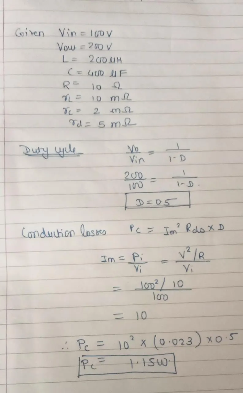
- Vin = 100 V
- Vout = 200 V
- L = 200uH
- C = 400uF
- R= 10 Ohms
- rL = 10 mOhms
- rC = 2 mOhms
- rd=5 mOhms
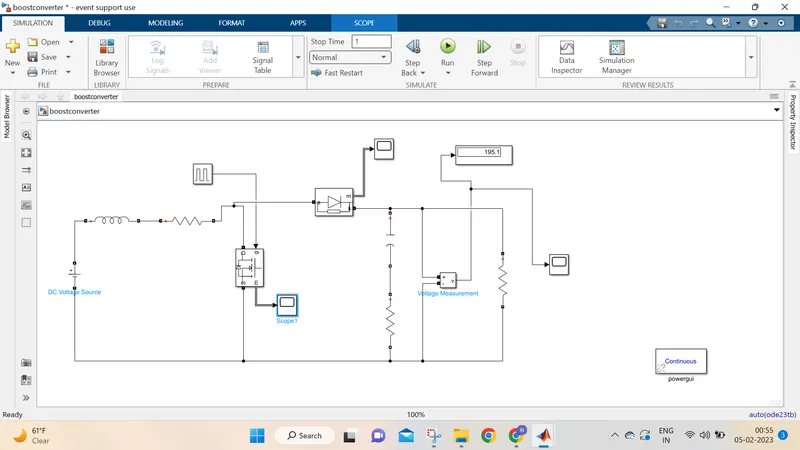
>For creating the Simulink model of the Boost converter The supply voltage and Series RL branch will be connected in series.
>.And MOSFET" acts as a power switch.
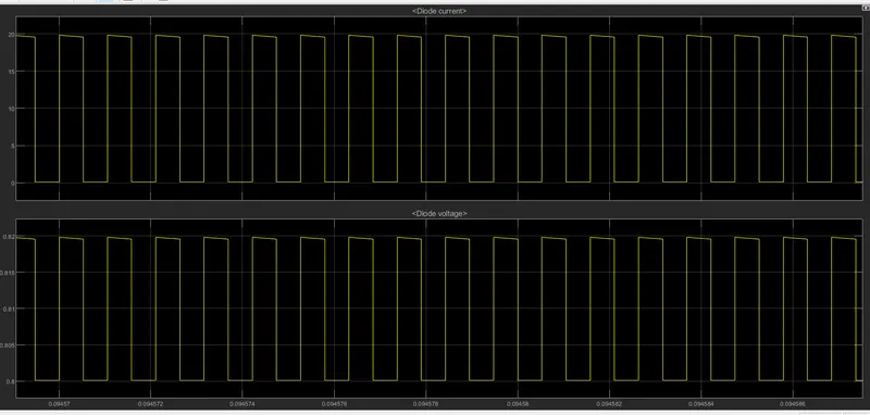
DIODE voltage and current:
MOSFET voltage and current:
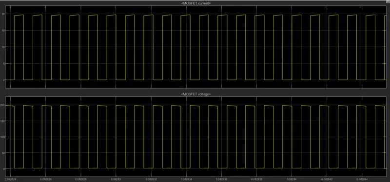
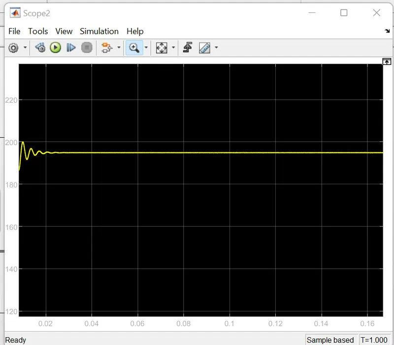
Result: From the above graph, we can see the Output voltage is greater than the Input voltage. The input voltage of 100v is boosted to 198 voltage.
The result can be verified from the scope as well as the display box.
Losses :
In any DC-DC converter majorly consider 4 types of losses are as followes:-
- Conduction Losses
- Diode losses
- Induction Losses
- Capacitor Losses
Conduction Losses:-
Conduction losses are a result of device parasitic resistances impeding the DC current flow in a DC/DC converter. These losses are in direct relationship with the duty cycle.
When the integrated high-side MOSFET turns on, the load current flows through it. The drain-to-source channel resistance (RDSON) causes power dissipation.
Formula:- conduction losses Pc=I^2*R*D......................(1)
where, I current through MOSFET
R Resistance in ohm
D duty cycle
Diode losses:-
The diode is forward-biased when the integrated MOSFET turns off. During this time, the inductor current ramps down through the output capacitors, the load and the forward-biased diode. Since the load current is now conducting through the diode, there will be power dissipation in Diode.
This will be calculated by using Formula:- P=Vf*I*(1-D)..........(2)
Vf=forward voltage
I =current output
D duty cycle
Induction Losses:-
The conduction losses depend on the load current. With heavier loads, the conduction loss in the MOSFET increases and is the dominating factor. Conduction losses plus switching, driver and internal low-dropout regulator (LDO) losses lead to a considerable generation of heat.
This loss can be calculated by using the formula: Pd=I^2*+(R1/R2)(D*Vin/f*L)
where I= Current
D duty cycle
f frequency
L= inductance
Capacitance losses:-
While getting the output through the capacitor we can get some power dissipation in the capacitor also.
this power dissipation is determined by using the Formula:-
Pc=rc*D(1-d)I^2+(RC/12(1-D)*(D/C*f)
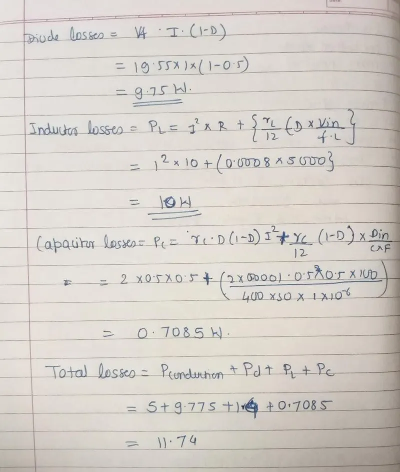
Total power losses =Pc+diode losses +inductor losses +capacitor losses
=11.74watt
Efficiency = Pout/Pin*100
=(1000-11.74)/1000*100
=98%