Project 1 - Loss calculation for a DC/DC converter-MATLAB
Aim:Loss calculation for a DC/DC converter-MATLAB
EV refresher Batch-5
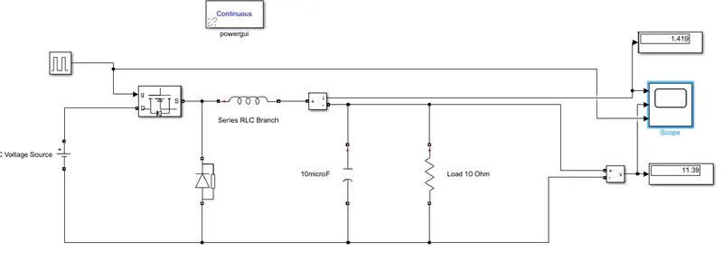
Simulink Model of Buck Converter
DC-DC converter is a converter which converts the dc voltage level of the input source into another DC voltage level. The DC-DC conversion can be done directly or can be done using alternative way.
The short and direct method is to convert DC-DC directly using Boost converter or buck converter. The working of the boost converter is to boost the input voltage while buck converter is used for reducing the input voltage level.
Buck converter is having a wide range of use in low voltage low power applications. Multiphase version of buck converters can provide high current with low voltage. Therefore, it can be used for low voltage high power applications.
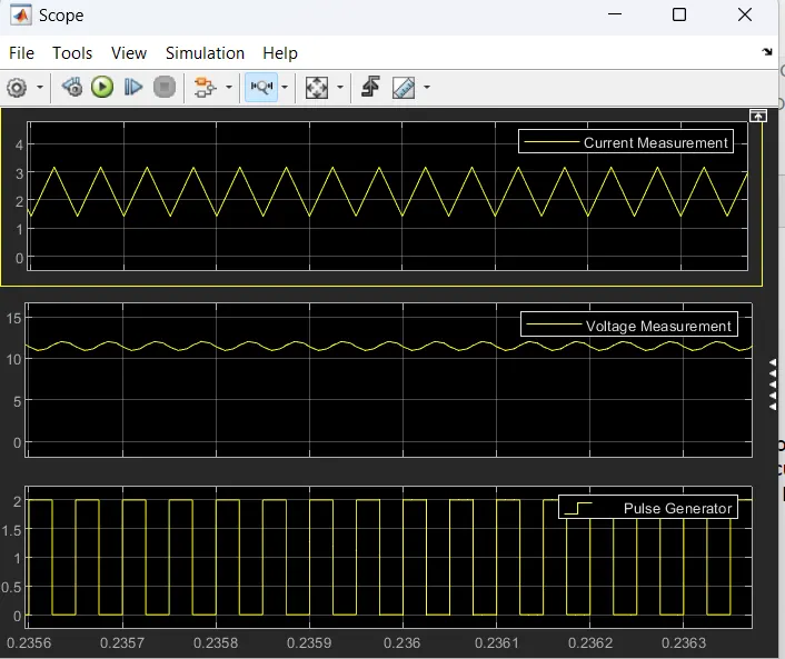
Result:
Power Losses
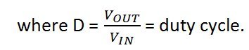
Conduction losses are a result of device parasitic resistances impeding the DC current flow in a DC/DC converter. These losses are in direct relationship with the duty cycle. When the integrated high-side MOSFET turns on, the load current flows through it. The drain-to-source channel resistance (RDSON) causes power dissipation, which can be expressed as Equation 1:

For nonsynchronous devices like the LM2673, the diode is forward-biased when the integrated MOSFET turns off. During this time, the inductor current ramps down through the output capacitors, the load and the forward-biased diode. Since the load current is now conducting through the diode, there will be power dissipation in it, expressed as Equation 2:

Where, VF is the forward voltage drop of the chosen diode.
In addition to the conduction loss in the integrated MOSFET and the catch diode, there are conduction losses in the inductor as well because every inductor has a finite DC resistance (DCR), which is the resistance of the wire in the coil. Equation 3 expresses the dissipation in the inductor as:

The conduction losses depend on the load current. With heavier loads, the conduction loss in the MOSFET increases and is the dominating factor. Conduction losses plus switching, driver and internal low-dropout regulator (LDO) losses lead to a considerable generation of heat and increase the junction temperature of the integrated circuit (IC). Equation 4 expresses the increase in junction temperature as:

where ICTj is the junction temperature of the IC, TA is the ambient temperature, θJA is the junction-to-air thermal resistance and ICPd is the total power dissipation just in the IC equal to .
The RDSON of the MOSFET typically has a temperature coefficient (RdsonTco). With an increase in the junction temperature of the IC, the RDSON would increase above the nominal based on the temperature coefficient. While this parameter may not be available in the data sheet, TI’s WEBENCH® Power Designer software has that information and uses it for calculating the design efficiency, thus making the results accurate. Equation 5 can adjust the RDSON based on the junction temperature:

where RdsonNom is the nominal value of RDSON as listed in the data sheet.
The increase in RDSON depends on how well the device is heat-sinked and on the junction temperature of the device. Improper heat-sinking can lead to a drastic increase in RDSON and cause a larger dip in efficiency at full load. This is evident in situations when the die attach paddle (DAP) of the IC is not well soldered to the board.
Calculating losses is an iterative process. You will need to evaluate the junction temperature and the resulting RDSON on every iteration of calculating the IC power loss to get accurate results in efficiency. WEBENCH Power Designer takes care of this; it displays the calculated results of passive component losses as well. Knowing these losses is important because it will help you choose the right components, along with a DC/DC regulator that will help maintain good efficiency. The total conduction losses can now be expressed as Equation 6:

Looking over all of the losses, Equation 7 adds them up to calculate the total loss:

Equation 8 expresses the resulting efficiency of the DC/DC buck converter design as:
