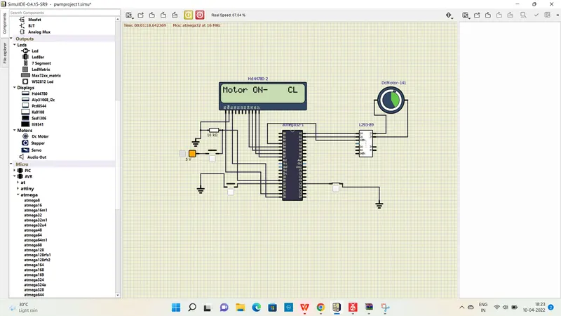
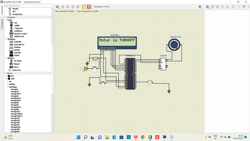
Project 1 - Controlling a DC motor using PWM and monitoring its Running status
Configuring Timer0 for PWM generation
It is simple to configure PWM mode in Timer. We just need to set some bits in the TCCR0 register.
TCCR0: Timer Counter Control Register 0
Bit 7- FOC0: Force compare match
Write only bit, which can be used while generating a wave. Writing 1 to this bit will force the wave generator to act as if a compare match has occurred.
Bit 6, 3 - WGM00, WGM01: Waveform Generation Mode
|
WGM00 |
WGM01 |
Timer0 mode selection bit |
|---|---|---|
|
0 |
0 |
Normal |
|
0 |
1 |
CTC (Clear timer on Compare Match) |
|
1 |
0 |
PWM, Phase correct |
|
1 |
1 |
Fast PWM |
Bit 5:4 - COM01:00:
- When WGM00: WGM01= 11 i.e. Fast PWM. Compare Output Mode
waveform generator on OC0 pin
|
COM01 |
COM00 |
Mode Name |
Description |
|---|---|---|---|
|
0 |
0 |
Disconnected |
The normal port operation, OC0 disconnected |
|
0 |
1 |
Reserved |
Reserved |
|
1 |
0 |
Non-inverted |
Clear OC0 on compare match, set OC0 at TOP |
|
1 |
1 |
Inverted PWM |
Set OC0 on compare match, clear OC0 at TOP |
2. When WGM00: WGM01= 10 i.e. Phase correct PWM. Compare Output Mode
waveform generator on OC0 pin
|
COM01 |
COM00 |
Description |
|---|---|---|
|
0 |
0 |
The normal port operation, OC0 disconnected |
|
0 |
1 |
Reserved |
|
1 |
0 |
Clear OC0 on compare match when up-counting, set OC0 on compare match when down-counting |
|
1 |
1 |
Set OC0 on compare match when up-counting, Clear OC0 on compare match when down-counting |
Bit 2:0 - CS02:CS00: Clock Source Select
These bits are used to select a clock source. When CS02: CS00 = 000, then timer is stopped. As it gets a value between 001 to 101, it gets a clock source and starts as the timer.
|
CS02 |
CS01 |
CS00 |
Description |
|---|---|---|---|
|
0 |
0 |
0 |
No clock source (Timer / Counter stopped) |
|
0 |
0 |
1 |
clk (no pre-scaling) |
|
0 |
1 |
0 |
clk / 8 |
|
0 |
1 |
1 |
clk / 64 |
|
1 |
0 |
0 |
clk / 256 |
|
1 |
0 |
1 |
clk / 1024 |
|
1 |
1 |
0 |
External clock source on T0 pin. clock on falling edge |
|
1 |
1 |
1 |
External clock source on T0 pin. clock on rising edge. |
Fast PWM mode
To set Fast PWM mode, we have to set WGM00: 01= 11. To generate a PWM waveform on the OC0 pin, we need to set COM01:00= 10 or 11.
COM01:00= 10 will generate Noninverting PWM output waveform and COM01:00= 11 will generate Inverting PWM output waveform.
Setting Duty cycle: we have to load value in the OCR0 register to set the duty cycle.
255 value for 100% duty cycle and 0 for 0% duty cycle. Accordingly, if we load value 127 in OCR0, the Duty cycle will be 50%.
Code:
/*
* pwmmotorp1.c
*
* Created: 10-04-2022 16:52:25
* Author : SS
*/
#include <avr/io.h> //we are using I/O registers of AVR
#define F_CPU 16000000L // define the crystal frequency
#include "avr/interrupt.h" // we are using external interrupt pin
#include <util/delay.h> // delay function purpose
#define sw_dir (PIND & (1<<1)) // d1 pin is declared as push button for direction control.
#define sw_dspd (PIND & (1<<2)) // d2 pin is declared as push button for speed control.
#define pw (PINC & (1<<3)) // c3 is declared as push button for power ON/OFF
#define lcd_port PORTB //PORTB pins are for LCD data
#define RS_high PORTD |= (1<<5) // d5 pin is used for Register Select(RS)
#define RS_low PORTD &=~ (1<<5) // d5 pin is used for RS
#define EN_high PORTD |= (1<<6) // d6 pin is used for Enable
#define EN_low PORTD &=~ (1<<6) // d6 pin is used for En.
unsigned char i;
void lcd_cmd(char cmd) //command for lcd display
{
lcd_port = (cmd & 0xf0); //4 bits for 4 bit lcd mode
RS_low;
EN_low;
_delay_ms(1); //after 1ms disable lcd
EN_high; //enable the lcd
lcd_port = ((cmd<<4) & (0xf0)); //lcd port
RS_low;
EN_low;
_delay_ms(1); //after 1ms disable lcd
EN_high; //enable the lcd
}
void lcd_data (char data) //send the data to lcd
{
lcd_port = (data & 0xf0); //4 bits for 4 bit lcd mode
RS_high; //access data register
EN_low;
_delay_ms(1);
EN_high;
lcd_port = ((data<<4) & (0xf0)); //4 bits for 4 bit lcd mode
RS_high; //access data register
EN_low;
_delay_ms(1);
EN_high;
}
void lcd_init()
{
lcd_cmd(0x28);// used for 4 bit lcd mode
_delay_ms(5);
lcd_cmd(0x02); // return home
_delay_ms(5);
lcd_cmd(0x01); // clear screen
_delay_ms(5);
lcd_cmd(0x0C); // display on cursor off
_delay_ms(5);
lcd_cmd(0x06); // increment the display cursor
_delay_ms(5);
lcd_cmd(0x80); // force cursor to begin from 1st line
_delay_ms(5);
}
void cursorpos(char x,char y)
{
if((x<1 || x>2) || (y>16 || y<1 )) //condition will checks the 2 rows and 16 columns
{
x=1; //x= row
y=1; //y= column
}
if(x==1)
{
lcd_cmd(0x7F + y); //{ 80-1 = 7F} for starting the 1st line hex decimal value (80) {y we r using the 7F+y means we need to dtart from that column}
}
else //(x==2)
{
lcd_cmd(0xBF + y); //{0C-1 = 0B} for starting the 2nd line, 2nd row.
}
}
void lcd_out(char x, char y, char *str) //here we are checking which position we want to print
{
cursorpos(x,y);
while(*str)
{
lcd_data(*str);
str++;
}
}
int adc_read(char channel) // we r configuring the adc value
{
unsigned int a, result;
ADMUX = channel; // here we r going to use which channel we need to select in mux here using 2 bit
ADCSRA = 0X80; //control & status register to enable the adc conversion ,enable the interrupt flag, adc interrupt. ADEN=1
ADCH = 0X00; // showing the value 0 or clearing the adc register
ADCL = 0x00; // showing the value 0
ADCSRA |= (1<<6); // to start the conversion 6 bit ADSC high
while((ADCSRA & 0x40) != 0); // when the conversion become zero means conversion of adc (0x40 means interrupted pin )
a= ADCL; //dummy data type a and ais stored the ADCL register (ADC0-ADC7)
result = ADCH; // Store the high value (ADC8-ADC9)
result = result<<8; //to get proper result or alined value we need to do left shift
result = result | a ; // we r adding the ADCL + ADCH to get the 16 bits
return result;
}
int main(void)
{
DDRB = 0XFF; //Declaring all 8-pins as output.
DDRA |= ((1<<0)| (1<<1)); //Declaring A0 & A1 pins as output.
DDRD &=~ (1<<1); //Declaring D1 pin as input.
DDRD &=~ (1<<2); //Declaring D2 pin as input.
DDRD |= (1<<5); //Declaring D5 pin as output.
DDRD |= (1<<6); //Declaring D6 pin as output.
DDRC &=~ (1<<3); //Declaring C3 pin as input.
PORTD |= (1<<2); //enabling internal pull up resistor for D2.
PORTC |= (1<<3); //enabling internal pull up resistor for D3.
i=64; //initializing i=64 because we are running the motor with 25% duty cycle.
TCCR0=0X61; //Non-Inverting mode, PWM phase correct mode,NO prescalar.
GICR=(1<<INT0); //using INT0 for interrupt
MCUCR=0X02; //make interrupt negative edge triggered
sei(); //Enable global interrupt
lcd_init(); //Initialize lcd
/* Replace with your application code */
while (1)
{
while(pw==0) //continue till the push button is released.
{
if(sw_dir == 0) //if the direction control push button is released.
{
PORTA = 0b00000001; // 1 0 to respective 1A 2A pins to rotate in clockwise direction.
lcd_out(1,1,"Motor ON- CL "); //Running clock wise direction
}
else
{
PORTA = 0b00000010; // 1 0 to respective 1A 2A pins to rotate in Anti-Clockwise direction.
lcd_out(1,1,"Motor ON- ACL");
}
OCR0 = i; //i increases in ISR, the corresponding value is to be loaded into OCR0.
}
PORTA = 0x00; // 0 0 to respective 1A 2A pins to Stop rotation.
lcd_out(1,1,"Motor is TURNOFF");
}
}
ISR(INT0_vect) //interrupt service routine
{
i=i+20; // as i increases the duty cycle also increases. i increases by 20 in each push//
// and the corresponding value is to be loaded into OCR0 in while loop//
}
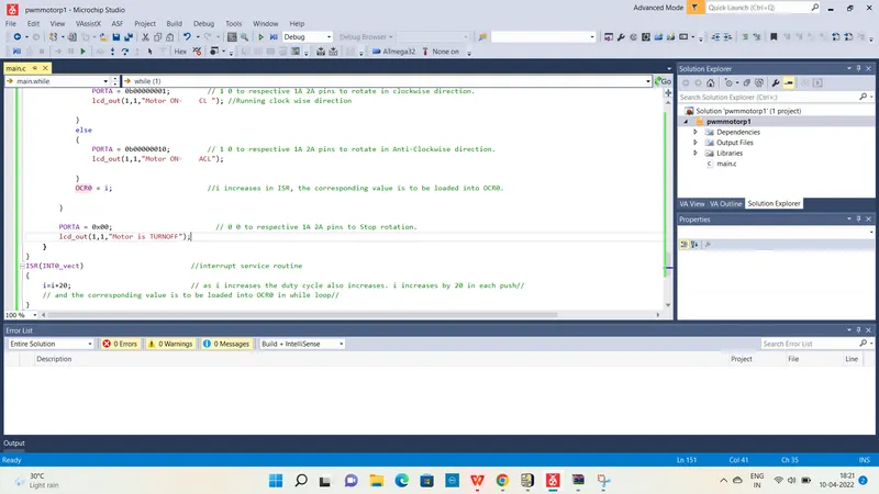
Motor in CLOCKWISE DIRECTION AT25 % DUTY CYCLE
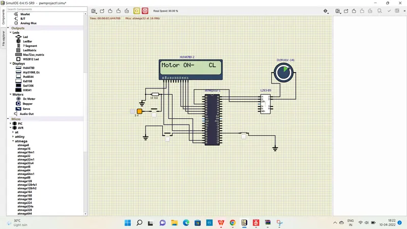
Motor in ANTICLOCKWISE DIRECTION
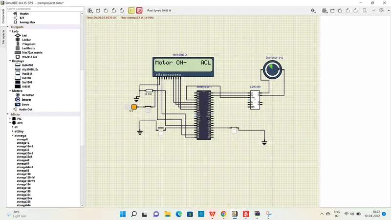
Dutycycle =60
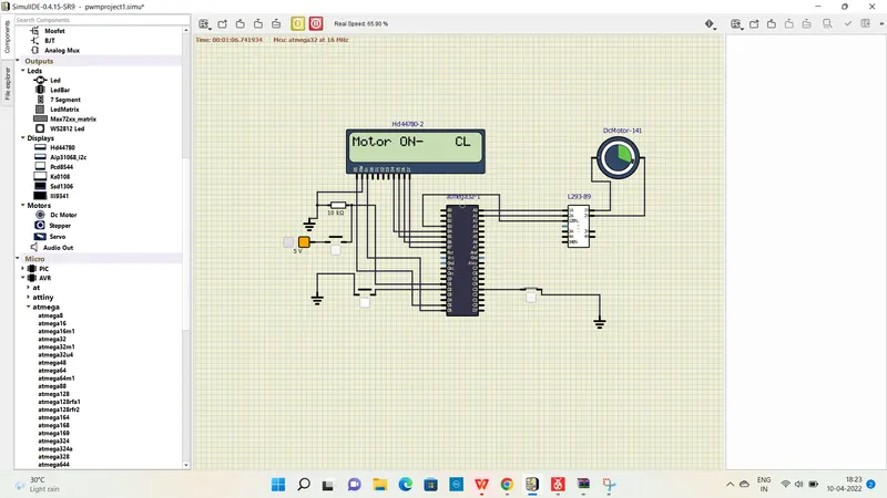
Duty cycle above 70%