Project 1
1. Buck Converter :
Buck converter in contious continous mode. Buck convertor does DC-DC conversion.Buck converter step down DC voltage. It consists of
Inductor, Capacitor and two switches which are transistor and diode.Transistor(moseft or igbt based on application) is a switch that operates
with on and off state. ON and OFF states get controlled by the Gate signal.
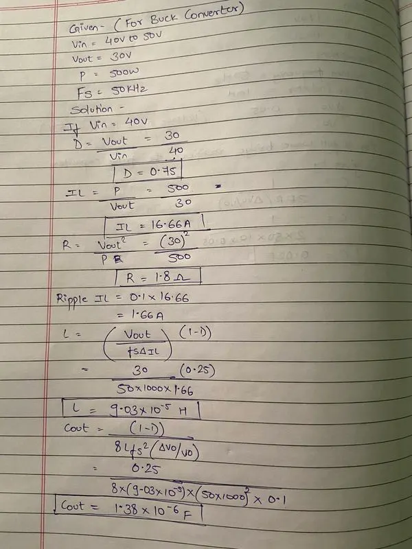
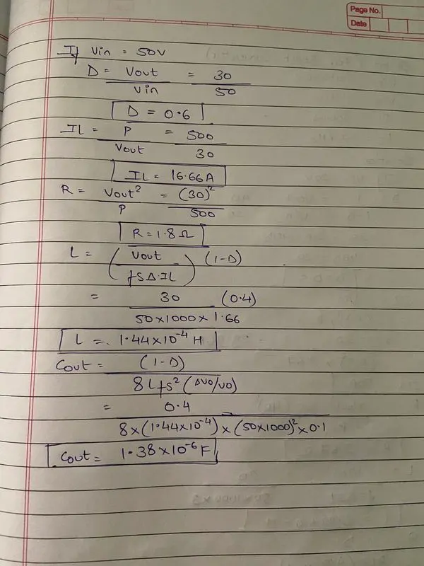
- Given :
Vin = 40 - 50V
Vout = 30V
P = 500W
Fs = 50KHz
- Calculation :
- Design and Simulation of Buck Converter :
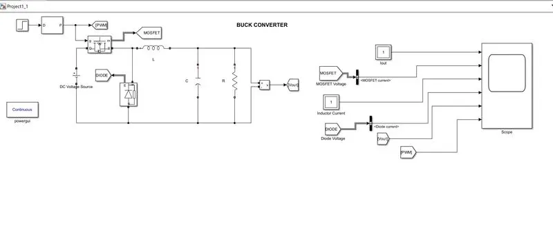
- This is the buck converter used to convert DC to DC with step down operation.
- The PWM Generator (DC-DC) block is used to pulse fire the MOSFET,GTO,IGBT switch of a one quadrant converter.
- The MOSFET block implements a macro model of the real MOSFET device.
- The Diode block implements a macro model of the real diode device.
- The Powergui block allow us to select one of these methods to solve are ciruit: Continuous or discrete phasor solution.
- The GOTO block passes its input to its corresponding from blocks.
- The Multimeter block measures the voltages and currents specified in the measurements parameter of simscape.
- The step block provides a step between two definable levels at a specified time.
- The scope block shows a strip chart/graph.
- Output Waveform (Result) :
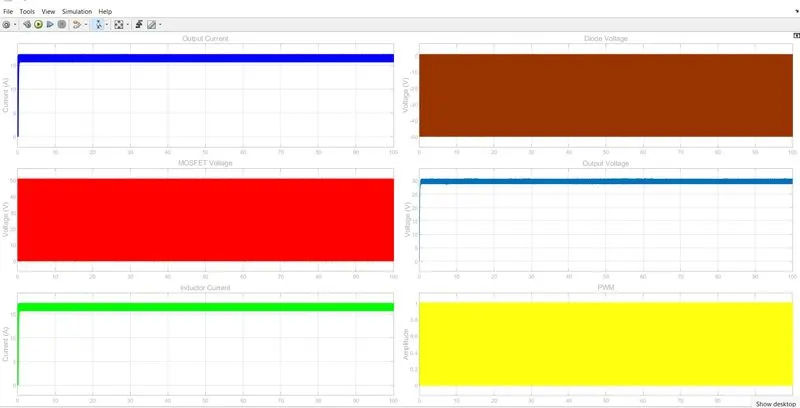
- Zoomed out output graph of buck converter.
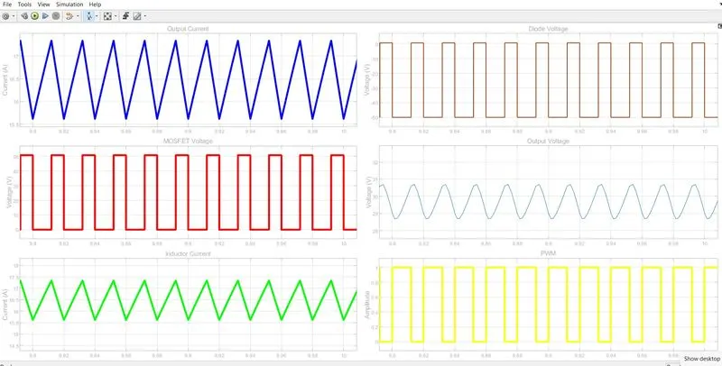
- Zoomed in output graph of buck converter.
- It shows that the output voltage 30V and the capacitor voltage is the same as output voltage.
- The MOSFET Voltage gradually increase till 50V then it stables for 0.5 sec then it gradually decreases till zero as shown in the graph.
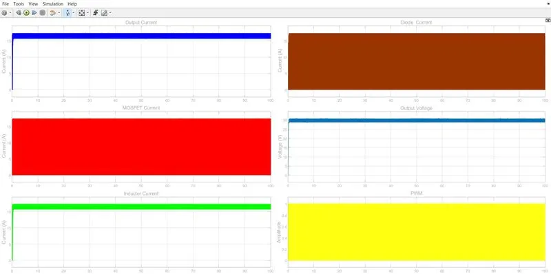
- Zoomed out output graph of buck converter.
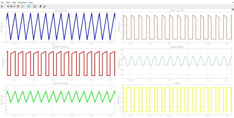
- Zoomed in output graph of buck converter.
- The inductor current has resulted as 17.5A.
- The vout represents the normal voltage in sine wave manner as shown in the graph.
- The Inductor current increases from 15.5A to 17.4A approx and decreases to 15.5A as shown in the graph.
- The Diode current gradually increases till 15.7A then it decreases to 15A and then it gradually decrases to zero as shown in the graph.
- Inductor and capacitor values are taken in such a way that the L and C values are high. As the input voltage range is from 40 to 50
as per the different input values, the inductor and capacitor values are designed accordingly.
2. Boost Converter :
The boost converter is the step up DC-DC converter. The output capacitor is the one that filters the pulsating current and allows DC current to
flow through the output.In continous conduction mode, the inductor current flows continously during the operation of the converter.The two
semiconductors during the operation of the converter. The two semi conductors switches in operation are diode and Mosfet which operate
with the PWM pulses. MOSFET is a switch whose gate pulses are given by the PWM pulse generator based on the duty requried to the switch.
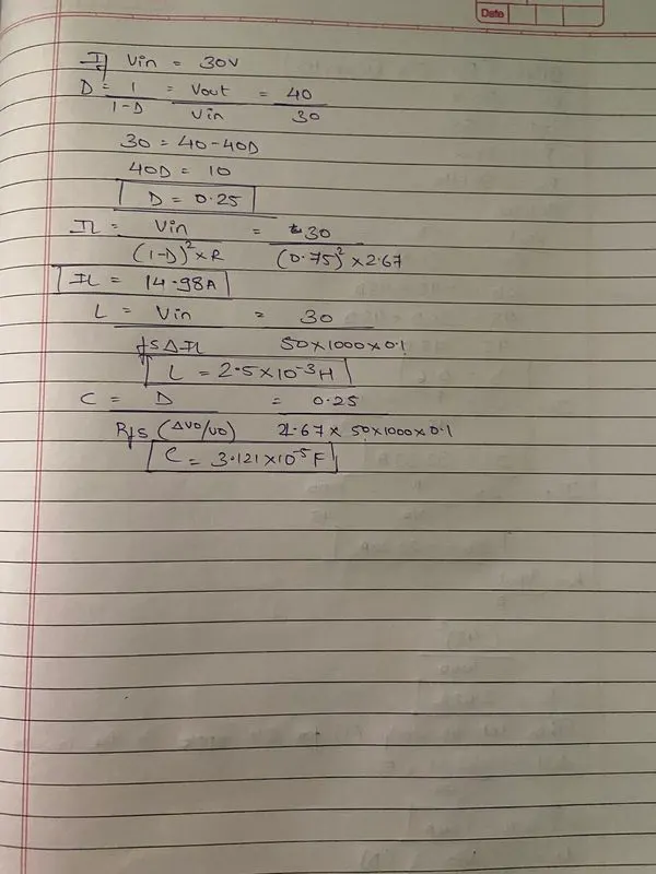
- Given :
Vin = 20 - 30V
Vout = 40V
P = 600W
Fs = 50KHz
- Calculation :
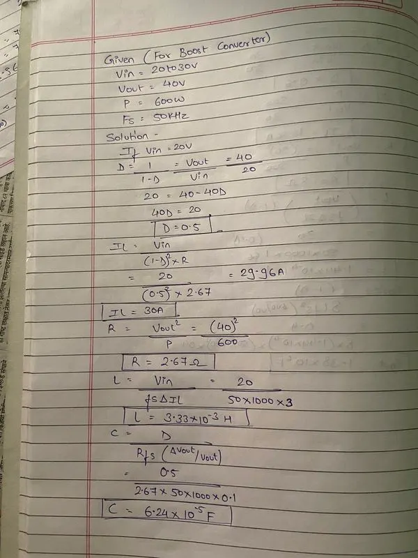
- Design and Simulation of Boost Converter :
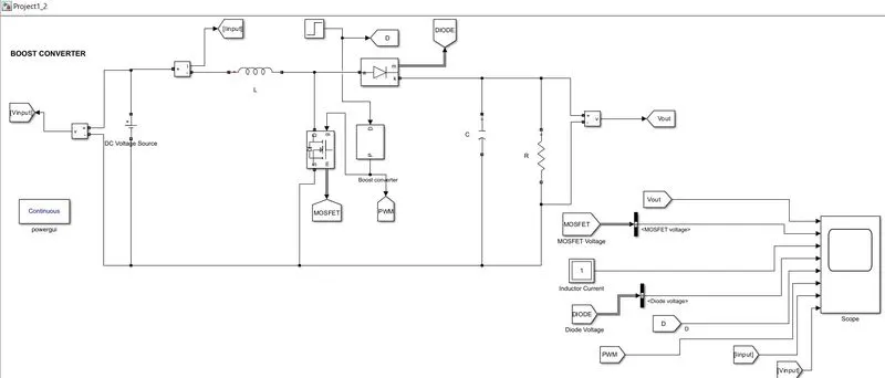
- The PWM Generator (DC-DC) block is used to pulse fire the MOSFET,GTO,IGBT switch of a one quadrant converter.
- The MOSFET block implements a macro model of the real MOSFET device.
- The Diode block implements a macro model of the real diode device.
- The Powergui block allow us to select one of these methods to solve are ciruit: Continuous or discrete phasor solution.
- The GOTO block passes its input to its corresponding from blocks.
- The Multimeter block measures the voltages and currents specified in the measurements parameter of simscape.
- The step block provides a step between two definable levels at a specified time.
- The scope block shows a strip chart/graph.
- The bus selector block outputs the elements you select from the input bus.
- Output Waveform (Result) :
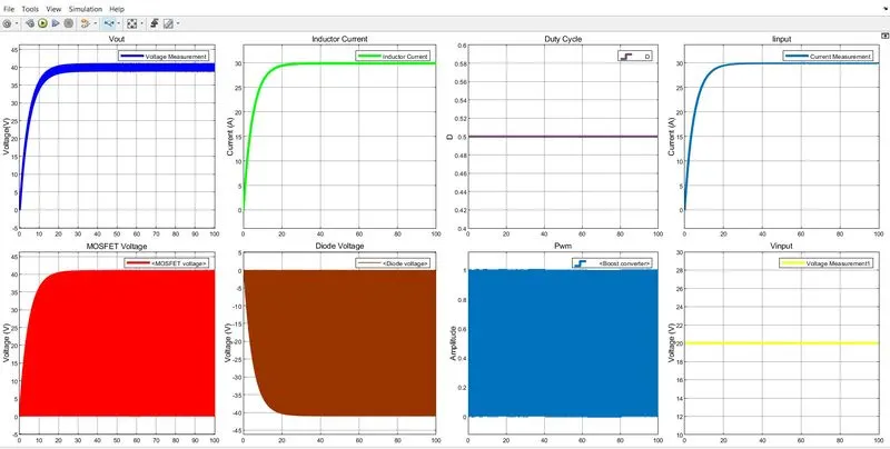
- Zoomed out output graph of boost converter.
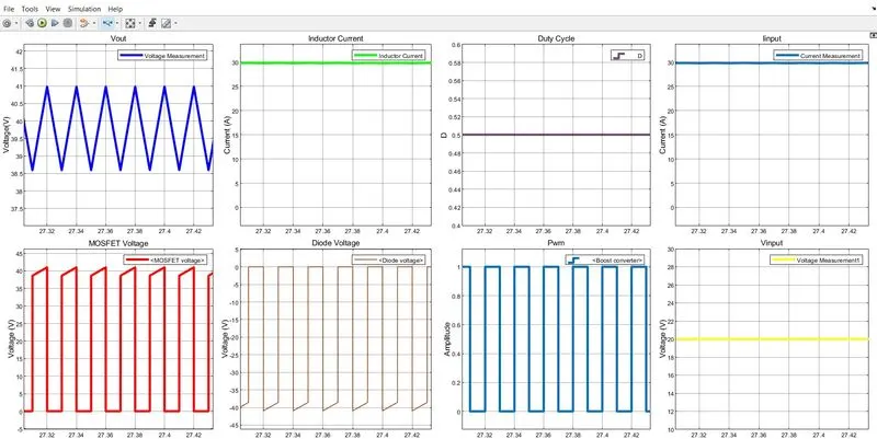
- Zoomed in output graph of boost converter.
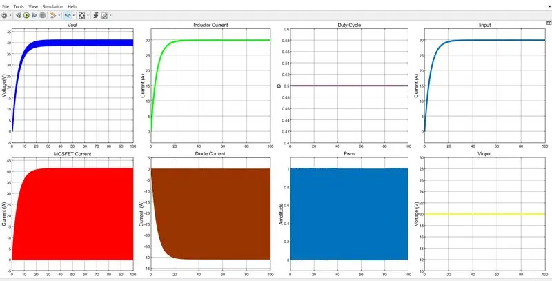
- Zoomed out output graph of boost converter.
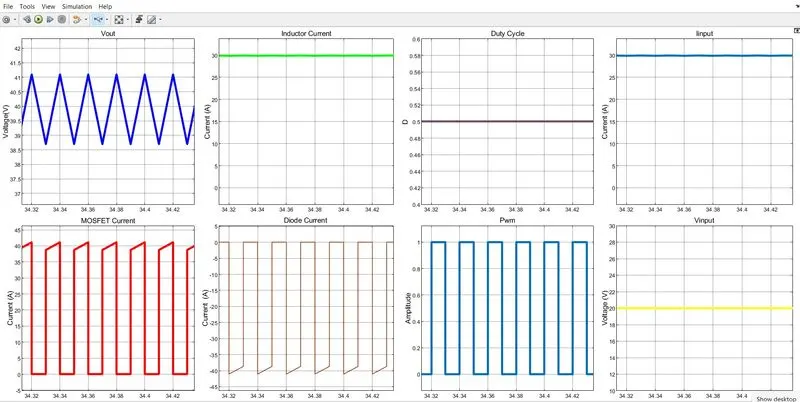
- Zoomed in output graph of boost converter.
- It shows the output voltage is 40V diode current and MOSFET current are showing that the switches are operating alternatively and PWM
signal is switching on when the MOSFET is ON and Mosfet is OFF when PWM signal is OFF.
- IDiode, Mosfet current and PWM signals are shown above for the input voltage of 20V to 30V.Output voltage is expected as 40V.And the
diode and current operates with different ON and OFF situations.
- Diode current is ranging upto -41A and MOSFET current is ranging upto 42A.Where the PWM pulses shows the ON and OFF states of the
MOSFET.
3. Cuk Converter :
Similar to the buck - boost converter with inverting topology, the output voltage of non-isolated cuk converter is typically inverted, with lower
or higher values with respect to the input voltage. Usually in DC converters, the inductor is used as a main energy-storage component. In cuk
converter, the main energy-storage component is the capacitor.
- Given :
Vin = 30 - 60V
Vout = -45V
P = 1KW
Fs = 50KHz
- Calculation :
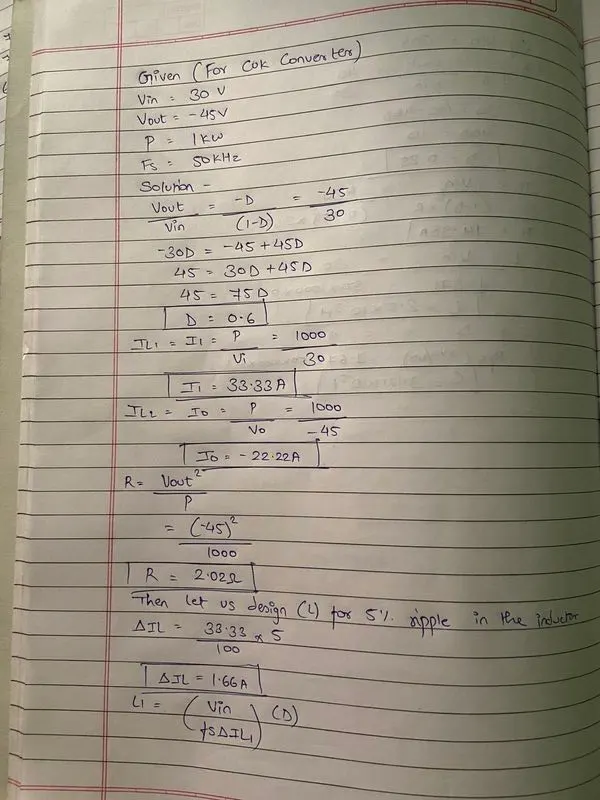
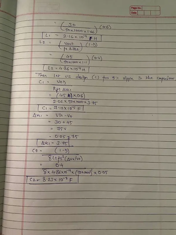
- Design and Simulation of Cuk Converter :
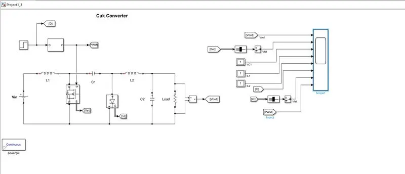
- The PWM Generator (DC-DC) block is used to pulse fire the MOSFET,GTO,IGBT switch of a one quadrant converter.
- The MOSFET block implements a macro model of the real MOSFET device.
- The Diode block implements a macro model of the real diode device.
- The Powergui block allow us to select one of these methods to solve are ciruit: Continuous or discrete phasor solution.
- The GOTO block passes its input to its corresponding from blocks.
- The Multimeter block measures the voltages and currents specified in the measurements parameter of simscape.
- The step block provides a step between two definable levels at a specified time.
- The scope block shows a strip chart/graph.
- The bus selector block outputs the elements you select from the input bus.
- Output Waveform (Result) :
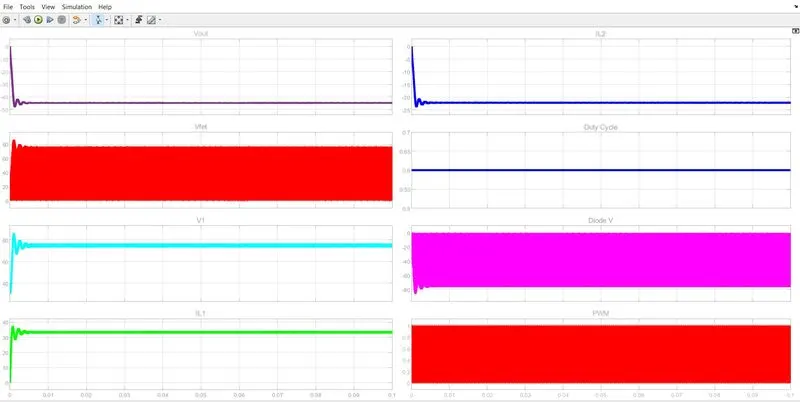
- Zoomed out output graph of cuk converter.
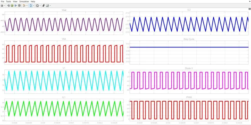
- Zoomed in output graph of cuk converter.
- The output voltage is -45.5V.
- The V1 voltage is 75.5V
- The IL1 increases to 34.2A and decreases to 32.2A. IL2 increases to -21.8A and decreases to -22.6A.
- The MOSFET Voltage is 81V and Diode Voltage is -79V.