Project 1
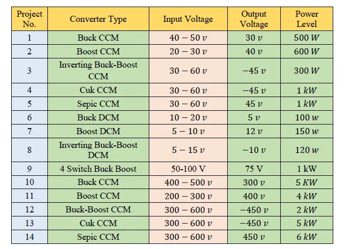
From the above mentioned topologies I have selected Project No. 4 ,5 and 7
Project 4 :- Here it was said to design a Cuk Converter which has a Input voltage which can vary between the range of 30-60V. Output voltage must be around 45 V in negative direction, and the power level for the converter is given as 1kW.
Assumption:-
Let the switching frequency of the converter be 50kHz.
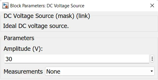
Let the input voltage be 30V.
Simulink Model:-
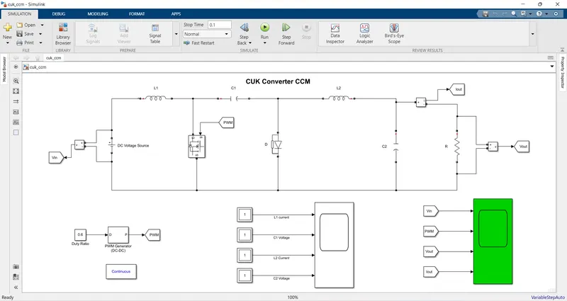
Block Used:- DC batery source, Series RLC branch, Mosfet, Diode, Current and Voltage Measurement, Goto and From block, Multimeter, PWM Generator, Constant, Powergui and Scope.
Component Calculation:-
i) Calculating the Duty ratio of the converter:-
For Cuk Converter duty ratio s given as:-
Vo/Vin = -D/ (1-D)
-45/30 = -D/ 1-D;
45 - 45D = 30D;
D= 45/ 75
D= 0.6
ii) Calculating △IL1 and △IL2
IL1= P/Vin = 1000/30 = 33.33 A
IL2= P/Vout= 1000/45 = 22.22 A
Load resistance (R) = (Vout^2)/P = (45*45)/1000= 2025/1000 = 2.025 Ω
For designing purpose let us assume that the ripple in the current at IL1 and IL2 is about 10% of the average Inductor Current, so
△IL1 = 0.1*33.33 = 3.33 A
△IL2 = 0.1*22.22 = 2.22 A
iii) Calculating Converter Inductance minimum value :-
Converter Inductance Minimum value is given by the expression as follows:-
L1> Vin*D / Fs*△IL1
L1> (30* 0.6) / (50000*3.33)
L1> 1.8/166.5
L1>0.010 mH
Also calculating minimum value of Inductor L2 as
L2> Vin*D / Fs*△IL2
L2> (30* 0.6) / (50000*2.22)
L2> 18/ 111
L2> 0.16 mH
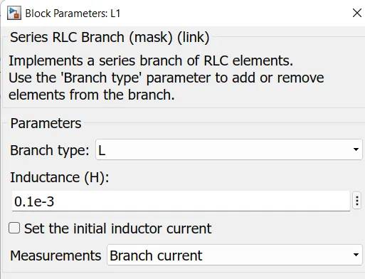
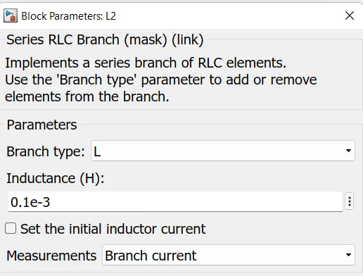
So lets assume the value of L1 and L2 to be = .1mH for operation in CCM .
Let, L1= L2= 0.1 mH
iv) Calculation of Intermediate capacitor:-
C1= Vo*D/ (R*fs*△Vc1)
also Vc1 = Vin - Vout
Vc1= 30- (-45)
Vc1= 75 V
For 10% volatge variation in Intermediate Capacitor voltage of the average Intermediate voltage,
Let △Vc1= 0.1*75 = 7.5 V
Now,
C1= (45 * 0.6)/ (2.025*50000*7.5)
C1= 27/ 759.375
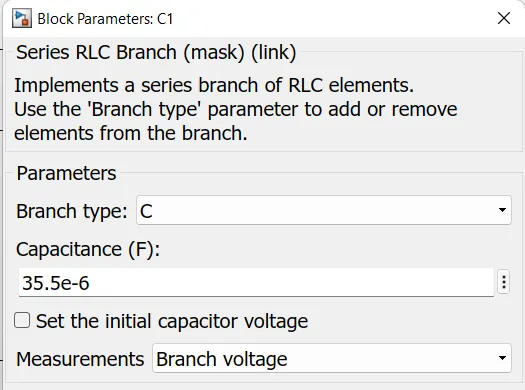
C1= 35.5uF
v) Calculation of Output Capacitor (C2)
C2= Cout= (1-D) / {8*L2*Fs*(△Vo/Vo)}
Let the capacitor be designed for 1% voltage ripple only then:-
C2= (1-0.6) / {8*0.0001*50000*50000*0.01}
C2= (4 x 10^-3)/ (8*25)
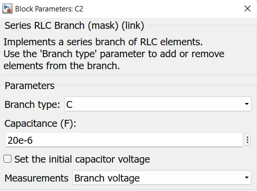
C2= 20uF
Now declaring all those value in the model made as follows:-
DC Volatge Source:-
Inductor L1:-
Intermediate Capacitor (C1):-
Inductor L2:-
Output Capacitor (C2):-
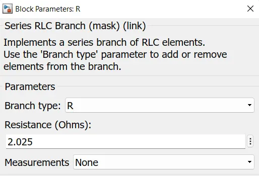
Load Resisatnce (R):-
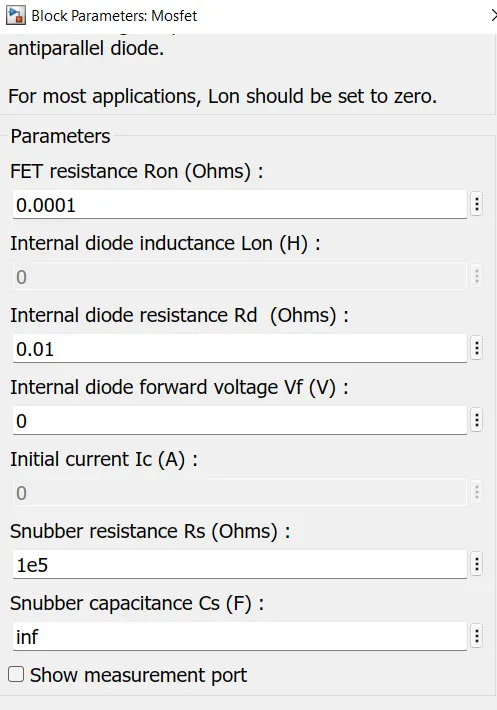
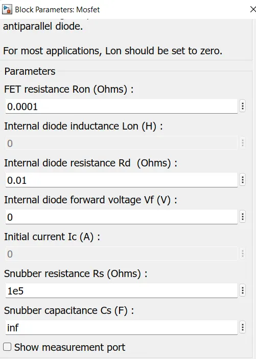
Mosfet:-
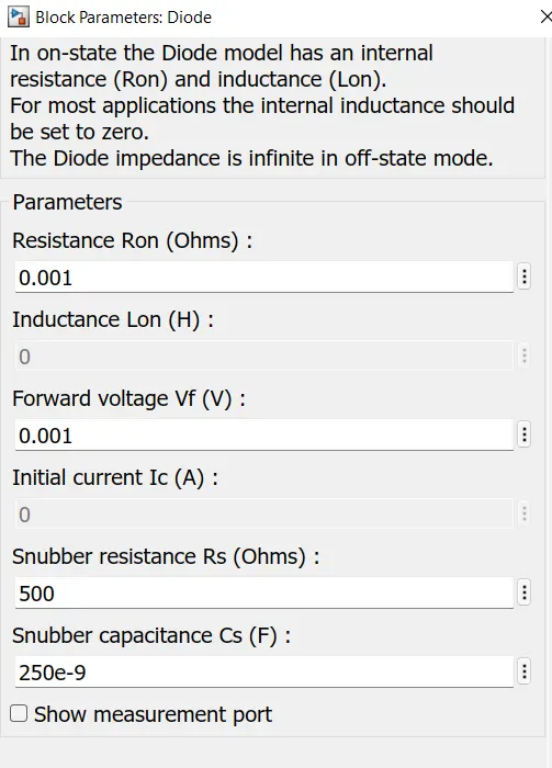
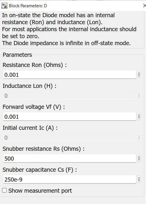
Diode:-
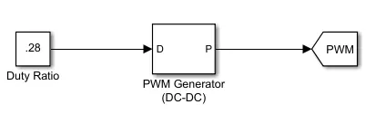
Gate Driver Circuit:-
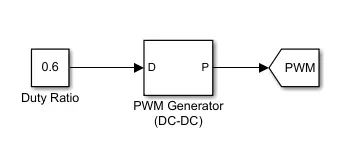
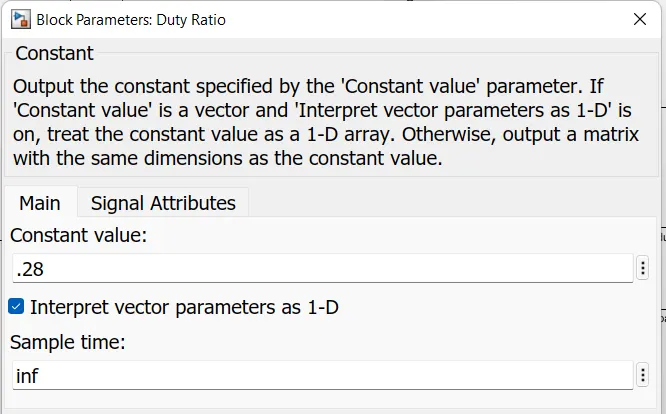
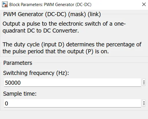
It consist of a constant block which will have the Duty ratio and then this constant block is fed through a PWM generator block which will have a frequency of around 50kHz and then this pulse is supplied across the Gate of the Mosfet.
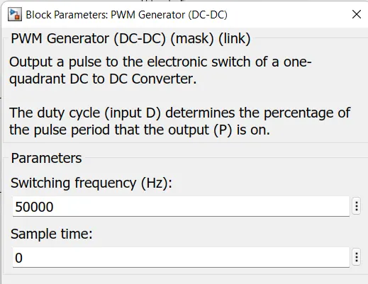
PWM Generator:-
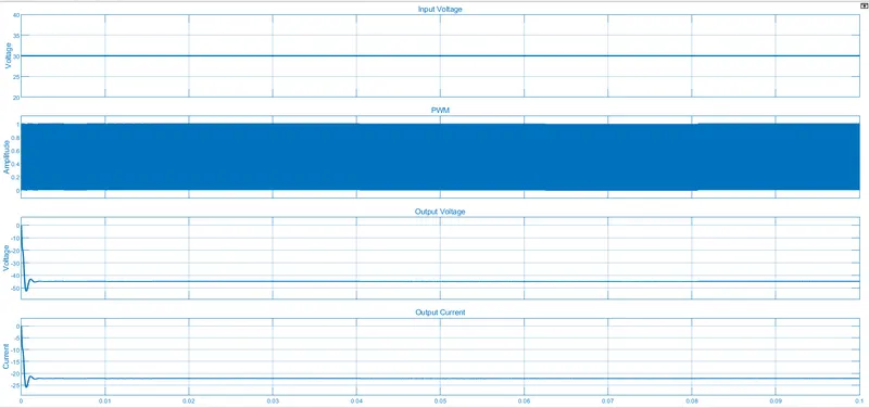
Result:- After assigning all the value of he components computed I tried to run the simulation for 0.1 sec.
The plot of Input voltage , PWM, Output volatge and Output Current is shown below:-
Zooming the above plot both in X and Y direction we get to see the plot as:-
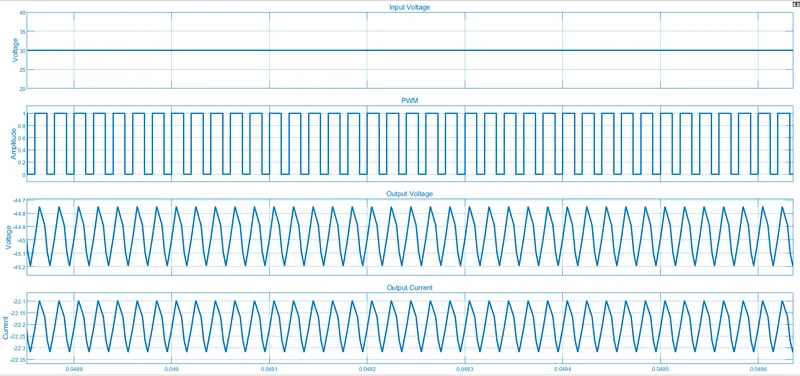
- The output voltage was -45 V and it varies between the value of -44.78 to -45.2 which is around 0.09% of the variation of the output volatge and we design it for the variation of about 1% which means that the converter is designed successfully.
Also the plot of Inductor Current and Capacitor Voltage is as shown below:-
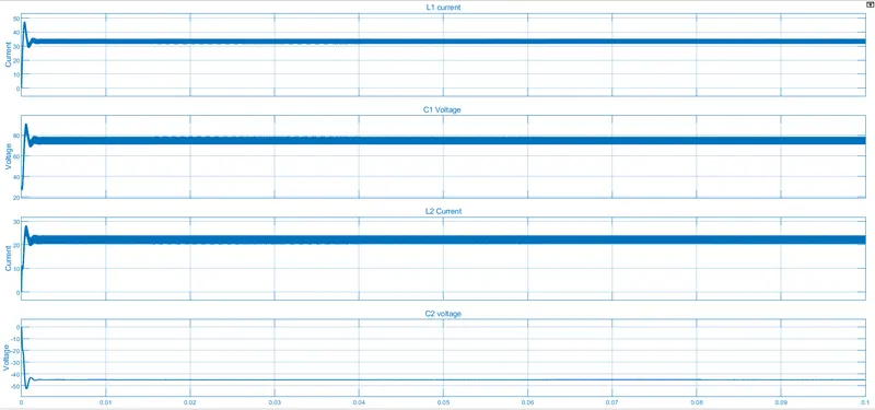
Zooming the above plot we get to see the plot as :-
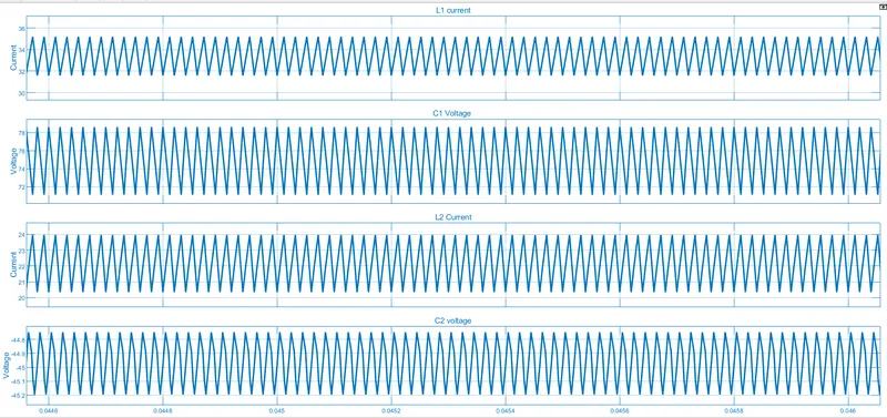
- The Inductor current L1 was 33.33 A and it was designed to have a ripple of 10%. It is avrying around 32 A to 35 A. So it was also designed as per the condition.
- The Inductor current L2 was 22.22 A and it was designed to have a ripple of 10%. It is avrying around 21.5 A to 24 A. So it was also designed as per the condition.
- The output voltage was -45 V around Capacitor C2 and it varies between the value of -44.78 to -45.2 which is around 0.09% of the variation of the output volatge and we design it for the variation of about 1% which means that the converter is designed successfully.
Project 5 :- Here it was said to design a Sepic Converter which has a Input voltage which can vary between the range of 30-60V. Output voltage must be around 45 V, and the power level for the converter is given as 1kW.
Assumption:-
Let the switching frequency of the converter be 50kHz.
Let the input voltage be 30V.
Simulink Model:-
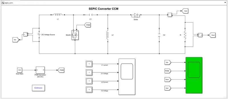
Block Used:- DC batery source, Series RLC branch, Mosfet, Diode, Current and Voltage Measurement, Goto and From block, Multimeter, PWM Generator, Constant, Powergui and Scope.
Component Calculation:-
i) Calculating the Duty ratio of the converter:-
For Sepic Converter duty ratio is given as:-
Vo/Vin = -D/ (1-D)
-45/30 = -D/ 1-D;
45 - 45D = 30D;
D= 45/ 75
D= 0.6
ii) Calculating △IL1 and △IL2
IL1= P/Vin = 1000/30 = 33.33 A
IL2= P/Vout= 1000/45 = 22.22 A
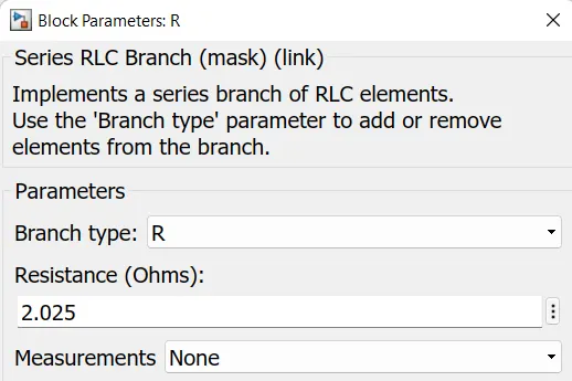
Load resistance (R) = (Vout^2)/P = (45*45)/1000= 2025/1000 = 2.025 Ω
For designing purpose let us assume that the ripple in the current at IL1 and IL2 is about 10% of the average Inductor Current, so
△IL1 = 0.1*33.33 = 3.33 A
△IL2 = 0.1*22.22 = 2.22 A
iii) Calculating Converter Inductance minimum value :-
Converter Inductance Minimum value is given by the expression as follows:-
L1> Vin*D / Fs*△IL1
L1> (30* 0.6) / (50000*3.33)
L1> 1.8/166.5
L1>0.010 mH
Also calculating minimum value of Inductor L2 as
L2> Vin*D / Fs*△IL2
L2> (30* 0.6) / (50000*2.22)
L2> 18/ 111
L2> 0.16 mH
So lets assume the value of L1 and L2 to be = .1mH for operation in CCM .
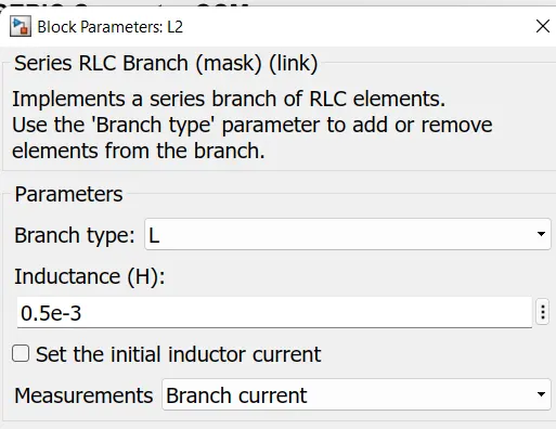
Let, L1= L2= 0.5 mH
iv) Calculation of Intermediate capacitor:-
C1= Vo*D/ (R*fs*△Vc1)
also Vc1 = Vin
Vc1= 30
For 10% volatge variation in Intermediate Capacitor voltage of the average Intermediate voltage,
Let △Vc1= 0.1*30 = 3 V
Now,
C1= (45 * 0.6)/ (2.025*50000*3)
C1= 27/ 303.75
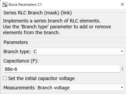
C1= 0.088mF = 88.8 uF
v) Calculation of Output Capacitor (C2)
C2= Cout= (D) / {R*Fs*(△Vo/Vo)}
Let the capacitor be designed for 1% voltage ripple only then:-
C2= (0.6) / {2.025*50000*0.01}
C2= (0.6x 10^-3)/ (1.0125)
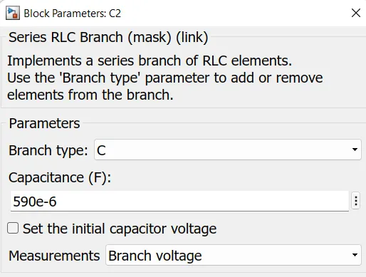
C2= 0.5925 mF= 592.5uF= 590uF
Now declaring all those value in the model made as follows:-
DC Volatge Source:-
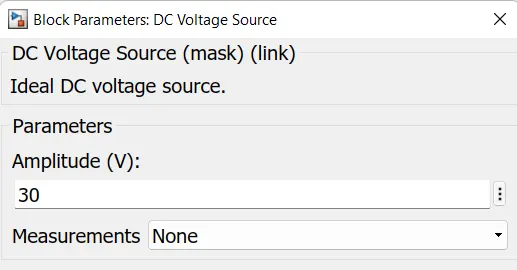
Inductor L1:-
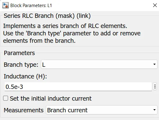
Intermediate Capacitor (C1):-
Inductor L2:-
Output Capacitor (C2):-
Load Resistance (R):-
Mosfet:-
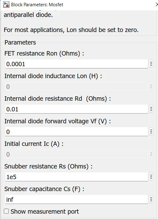
Diode:-
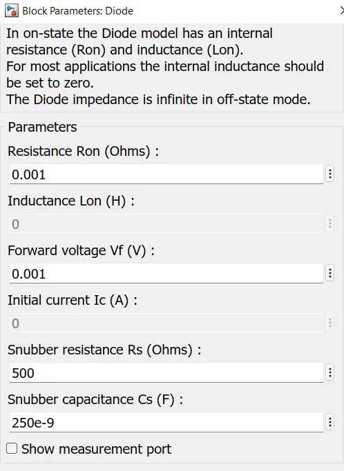
Gate Driver Circuit:-
It consist of a constant block which will have the Duty ratio and then this constant block is fed through a PWM generator block which will have a frequency of around 50kHz and then this pulse is supplied across the Gate of the Mosfet.
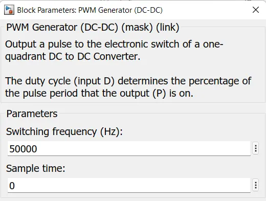
Result:- After assigning all the value of he components computed I tried to run the simulation for 0.1 sec.
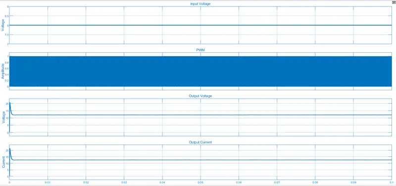
The plot of Input voltage , PWM, Output volatge and Output Current is shown below:-
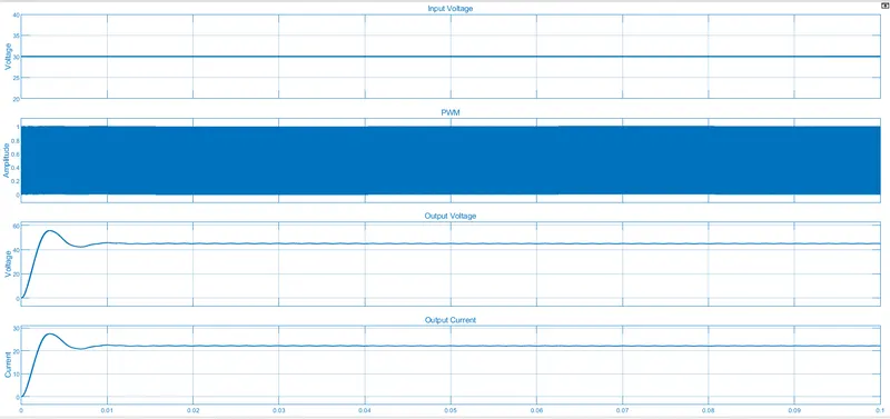
Zooming the above plot both in X and Y direction, we get
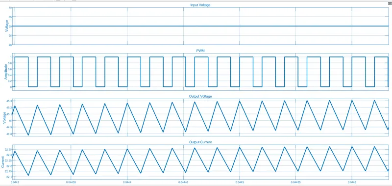
- The output voltage was 45 V and it varies between the value of 44.8 to 45.2 which is around 0.08% of the variation of the output volatge and we design it for the variation of about 1% which means that the converter is designed successfully.
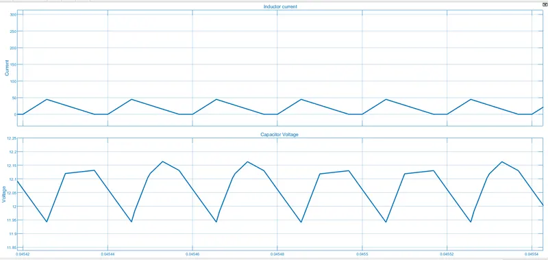
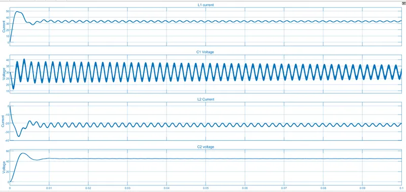
Also the plot of Inductor Current and Capacitor Voltage is as shown below:-
Project 7 :- Here it was said to design a Boost Converter in DCM which has a Input voltage which can vary between the range of 5-10V. Output voltage must be around 12 V, and the power level for the converter is given as 150W.
Assumption:-
Let the switching frequency of the converter be 50kHz.
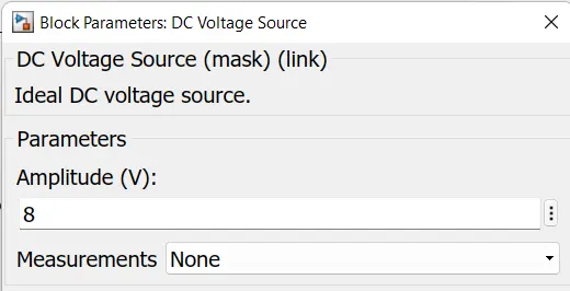
Let the input voltage be 8V.
Simulink Model:-
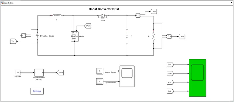
Block Used:- DC batery source, Series RLC branch, Mosfet, Diode, Current and Voltage Measurement, Goto and From block, Multimeter, PWM Generator, Constant, Powergui and Scope.
Component Calculation:-
i) Calculating the Duty ratio of the converter:-
For the Boost converter duty ratio is given as:-
Vout/ Vin= 1 / (1-D)
12/ 8 = 1 / (1-D)
12 - 12D = 8
D= 4/12
D= 0.33
ii) Calculating the Output Current and Load Resistance of the converter:-
Iout= P/Vout = 150/ 12 = 12.5 A
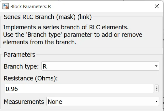
Load Resistance (R) = Vout^2/ P = 12*12/ 150 = 144/150 = 0.96 Ω
iii) Calculation of Minimum Inductance value for the converter:-
Lmin= {D *((1-D)^2)* R} / 2*Fs
Lmin= 0.33 * 0.66*0.66* 0.96 / 2* 50000
Lmin = (0.1379x 10^-3) / 100
Lmin= 1.37uH
For the converter to work in DCM mode we have four condition:-
- DCM Inductance value must be less than the minimum value of Inductance for the CCM mode.
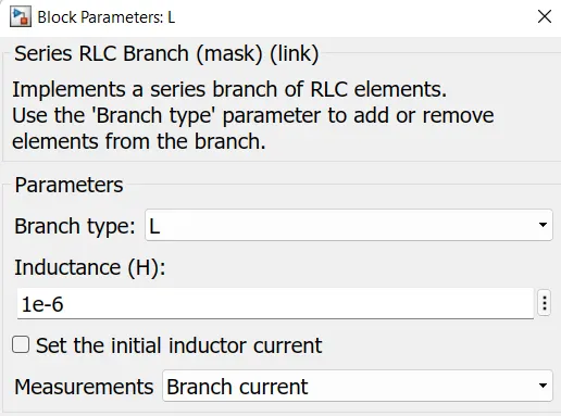
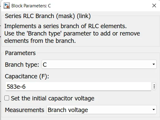
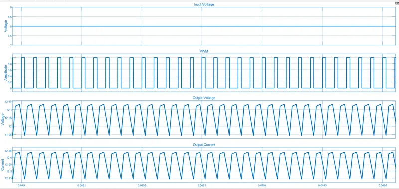
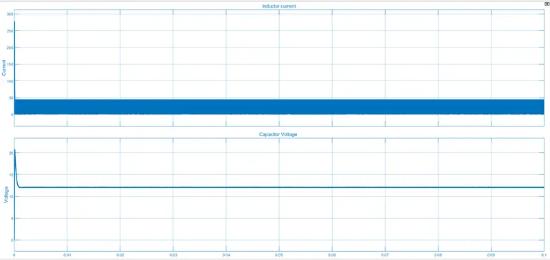
Ldcm ILmin<0 △IL> 2IL D1< 1-D So, by selecting any of the one condition and designing the converter based on the abov condition we can deisgn the converter to work in DCM. Therefore selecting the Inductance value less than the Lmin I have selected value of L = 1uH. i) We have to calculate the new duty ratio for the converter to operate in DCM mode for rated 12V output and 8V input supply. The expression for the same can be given by the following expression:- Vo/Vin= 1+ (sqrt(1+(4(D*D)/K))/2--------------------------(a) where K can be given by; K= 2L/TR where T is theime period and is 1/Fs so, K= 2LFs/R K= 2* (1x10^-6)*(50*10^3) / 0.96 K= (100x 10^-3) / 0.96 K= 0.104 Putting value of K in eq (a) we get 12/ 8 = 1+ (sqrt(1+4(D*D)/0.104))/2 1.5*2= 1+(sqrt(1+38.46D*D) 3-1 = (sqrt(1+38.46D*D) 2= (sqrt(1+38.46D*D) squaring both side we get, 4= 1+38.46D*D 3= 38.46 D^2 D^2= 0.078 D= 0.279 = 0.28 D=0.28 iii) Calculating Converter Capacitor value:- Cout= D / (R*Fs*△Vo/Vo) Considering change in output volatge is about 1% so, we get the value of C as:- C= 0.28/ (50000*0.96*0.001) C= 0.26x10^3/ 0.48 C= 0.583 mF = 583uF Now declaring all those value in the model made as follows:- Dc Voltage Source:- Inductor :- Capacitance:- Load Resistance (R):- Mosfet:- Diode:- Gate Driver Circuit:- It consist of a constant block which will have the Duty ratio and then this constant block is fed through a PWM generator block which will have a frequency of around 50kHz and then this pulse is supplied across the Gate of the Mosfet. Result:- After assigning all the value of he components computed I tried to run the simulation for 0.1 sec. The plot of Input voltage , PWM, Output volatge and Output Current is shown below:- Zooming the above plot both X and Y direction, we get:- Also the plot of Inductor Current and Capacitor Voltage is as shown below:- Zooming in X direction we get to see the below plot:- It is clearly visible that the Inductor current is dicontinuous and reaches to zero before the Toff time is raeched. Hence the converter work in the DCM of operation and the converter model for 12V output is successfully craeted.