Project 1 - 40-V to 80-V adjustable output voltage boost reference design for LIDAR applications
PCB can have single multiple layers of dielectric and conductive materials. These layers when attached with each other, they carry electrical circuits which sometimes linked with each other. According to applications like home electronics, alarm clocks, other household appliances, computers and mobiles. Printed circuit board has also extended its applications with industrial tools and machinery, in most of the medical devices, storage systems and aerospace industry. The number of layers and its dimensions determined by PCB distribution power device.
Five factors are there which are required to be considered before selection of number of layers:
- 1) Applications: It is very important to identify the purpose. Types of machines, complexity of the electronics circuit and power demand.
- 2) Operation frequency:It is also important to determine the operation frequency of the application. Operation frequency of any application indicates the function and the capacity of the printed circuit board. For higher processing speed and capacity is required.
- 3) Economy:Manufacturing cost is another parameter in this list. As the layers are going to increase, so will the cost. If applications required a higher processing speed and capacity then the cost will also escalate.
- 4) Manufacturing time:this talk about the lead time, that means time to manufacture single or multiple layer printed circuit board. This lead time effect all above mentioned parameters.
- 5) Density:The density will also decide the selection of layers. There is another term which is known as pin density. If the pin density is 1, it suggests that printed circuit board must be of single layer. As pin density decreases the number of layers increases. For example; if the value of pin density is 0.2, there is need of at least ten layers in printed circuit board.
PCB stack up principle:
After the required numbers of layers are determined, the following tasks are required to be completed carefully. So that all circuits are arranged reasonably. There are two required factors:
- Special signal layers distribution.
- Proper distribution of power layer and ground layer.
There could be more possible arrangements for ground layer, power layer and special signal layer as the number of layers. But there are certain principles to make these arrangements of layers:
- 1- The special signal layer should be next to the power layer. Shielded with copper power layer.
- 2- Two avoid the direct contact between two signal layers, a ground layer can be placed between them.
- 3- Multiple ground layer and power layers can reduce impedance effectively.
- 4- The symmetry of layer structure.
To calculate trace width:
PCB - nets - all nets- click the trace required - properties window - width is given
IPC-2221 is generally accepted in electronic industry as a generic PCB design standard. However, when it comes to distances between the PC traces, in my view, the IPC-2221 table 6-1 stepwise limits are mostly baseless: the curve for spacing vs. voltage should be linear. Of course, it is not the only standard that defines the electrical clearance. For power conversion circuits IPC-9592 initial draft provided the following linear circuit board spacing recommendations: SPACING (mm) = 0.6 + Vpeak x .005. In general, a linear relationship makes more sense. However, these requirements were also too conservative and at low voltages were not even practically doable. The updated IPC-9592B document left the above equation only for V≥100V. At other voltages the limits are as following: 0.13mm for V<15V, 0.25mm for 15V≤V<30V and 0.1+Vpeak×0.01 for 30V≤V<100V. Note that all IPC standards are voluntarily rather than mandatory. Conversely, for the products covered by safety standards the creepage and clearance requirements of a respective UL/IEC standard are mandatory. For example, for most ITE applications you need to use UL 60950-1 Tables 2K to 2N.
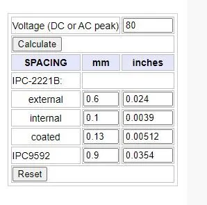
As a reference, the chart below compares PCB distance limits based on the following three specs for external layers of uncoated bare boards;
- IPC2221B
- IPC9592B;
- UL60950 for functional insulation in secondaries, designed to meet the test per Table 5B with the assumption of 40V/mil withstand voltage.
to calculate trace lenght:
panel - pcb - nets - all nets - click the trace to which lenght is to be calculate - lenght is provided there
Via Sizing Calculations and Charts
Absolute via sizes are not really specified according to industry standards. Instead, only the minimum sizes are specified based on the size of the component that will be mounted on the via. These standards must be followed if your PCB is to be compliant. The IPC-2222 standard specifies minimum hole diameters for plated through-hole vias for different classes of vias as follows:
- Minimum hole size = Maximum lead diameter + 0.25 mm (Level)
- Minimum hole size = Maximum lead diameter + 0.20 mm (Level B)
- Minimum hole size = Maximum lead diameter + 0.15 mm (Level C)
If you’re not familiar with this terminology, the lead diameter refers to the size of pin on a component that will appear on a particular plated through-hole via.
In addition to standard via sizes, there are also standardized pad sizes that should be used in compliant PCBs. The IPC-2221A standard defines minimum pad sizes for vias as a + 2b + c, where a is the maximum hole diameter, minimum annular ring size, and c is the fabrication tolerance. The fabrication tolerance depends on whether the vias are mechanically drilled or laser drilled, as well as individual process and machining parameters.
The maximum fabrication tolerances are defined as 0.6 mm for Level A, 0.5 mm for Level B, and 0.4 mm for Level C. If your manufacturer’s tolerance is less than 0.4 mm, your vias can meet the highest level of certification. Manufacturers usually have different processes that are designed to meet each level.
Each of the levels above refers to a particular “density level.” Level A is used for boards component with low density and components with a large footprint. Level B is a standard density level that is suitable for reflow, wave, drag, or dip soldering. Finally, Level C is used for HDI boards with very small, dense components.
If you’re not in the mood to pull out a calculator, you can find charts that tabulate this information on the internet. If your vias involve a larger current and might contribute to IR losses, you’ll want to use vias that are somewhat wider and fill them with a conductive epoxy. This will help you exceed the industry standards on via sizes. The filled via will prevent solder from wicking through the via hole and onto the bottom of the board when mounting through-hole components.
The main drawback of 2 Layer PCBs is that they are not as durable as other types of PCBs. In other words, 2 Layer PCBs are also more susceptible to crosstalk and noise than other types of PCBs.
And the disadvantages of double-sided boards are as follows:
-Firstly, they are more expensive to manufacture than single-sided boards.
-In addition, they require more solder mask layers and thus have a longer manufacturing production process.
-Also, the through-hole vias can be difficult to solder.
-Besides, the manufacturing of double-sided PCB is more difficult than that of single-sided PCB.
-Last but not least, the yield rate of double-sided PCB is lower than that of single-sided PCB.
In short, the disadvantages of double-sided PCB include higher price, longer manufacture process, more difficulty to solder, and lower yield rate.